
 Open Access Article
 This Open Access Article is licensed under a
 Creative Commons Attribution 3.0 Unported Licence
Perovskite single pixel imaging exceeding the visible towards X-ray and THz
Xuanqi
Wang†
a,
Lizhi
Ren†
bc,
Huiyi
Zong
bd,
Congcong
Wu
 *c,
Jin
Qian
*bd and
Kai
Wang
*bde
*c,
Jin
Qian
*bd and
Kai
Wang
*bde
aZJU-UIUC Institute, Zhejiang University, Haining 314400, China
bHuanjiang Laboratory, Zhuji 311800, China. E-mail: jqian@zju.edu.cn; kaikaiwang@zju.edu.cn; kaiwang@psu.edu
cKey Laboratory for the Green Preparation and Application of Functional Materials, Key Laboratory of Polymer Materials, School of Materials Science and Engineering, Hubei University, Wuhan 430062, China. E-mail: ccwu@hubu.edu.cn
dSchool of Aeronautics and Astronautics, Zhejiang University, Hangzhou 310027, China
eDepartment of Materials Science and Engineering, Pennsylvania State University, University Park, PA 16802, USA
First published on 29th June 2024
Abstract
Images are traditionally interpreted through a series of spatial pixels, as exemplified by digital imaging chips that rely on silicon-based CCD and CMOS sensor technologies. However, because of the intrinsic material limitations of silicon, extending the imaging capabilities of higher signal-to-noise ratios under weak-light conditions, or to encompass gamma- and X-rays, and terahertz spectral regions presents significant challenges. Recently conceptual single-pixel imaging (SPI) represents a novel paradigm in image interpretation, offering a viable alternative that bypasses the intricate manufacturing requirements of multi-pixel arrays and enables the use of advanced, non-silicon materials. Halide perovskite emerges as a notable alternative, acclaimed for its superior photonic detection capabilities across a broad spectrum beyond the visible and its promising performance level higher than that of the state-of-the-arts. We propose that the perovskite-based SPI has the potential for cost-effective and multi-spectral imaging solutions to the existing techniques. This paper delves into the transformative impact of perovskite-based SPI, with discussions of its fundamentals, detailed imaging manifestations in different spectral regions, and its promising role in revolutionizing photonic imaging towards bidirectional extension far beyond the visible spectrum.
 Xuanqi Wang | Xuanqi Wang is a student at Zhejiang University (ZJU) and University of Illinois Urbana-Champaign (UIUC), majoring in Electrical Engineering. His research interests involve signal processing, material science, and reinforcement learning. |
 Lizhi Ren | Lizhi Ren is currently a master's student under the supervision of Professor Congcong Wu at Hubei University and an exchange intern at Huanjiang Laboratory. His research interest is the synthesis of perovskite materials and their application in flexible electronics. |
 Huiyi Zong | Huiyi Zong is a doctor's candidate at Zhejiang University. She received her mechanical BS degree from Dalian University of technology in 2023. Her research focuses on mechanical and optical properties of soft lattice materials and their device applications. |
 Congcong Wu | Dr Congcong Wu is currently a Professor in Materials Science and Engineering, Hubei University. He received his BS degree and PhD degree in Materials Science and Engineering from Huazhong University of Science and Technology in 2007 and 2014, respectively. From 2014 to 2018, he worked as a research associate at the Center for Energy Harvesting Materials and Systems (CEHMS) at Virginia Tech, United States. Then he worked as an associate research professor in materials science and engineering, at the Pennsylvania State University, United States, from 2018 to 2019. His research interests include photovoltaic materials and device, 2D inorganic–organic hybrid materials, flexible electronics, biomimetic materials and devices etc. |
 Jin Qian | Dr Jin Qian, Professor and Vice Dean of the School of Aeronautics and Astronautics at Zhejiang University, currently serves as the Deputy Director of Huanjiang Laboratory and the Director of the Zhejiang Provincial Key Laboratory for Soft Robotics and Intelligent Devices. Dr Qian is a council member of the Chinese Society of Theoretical and Applied Mechanics, serving as the Deputy Head of the Soft Matter Mechanics Working Group. His research has primarily focused on the interdisciplinary fields of soft matter mechanics and 3D printing, biomechanics and biomimetics, as well as cell mechanics and cell adhesion. |
 Kai Wang | Dr Kai Wang, a researcher at Huanjiang Laboratory, currently serves as an assistant professor in the School of Aeronautics and Astronautics at Zhejiang University. He earned his PhD in polymer engineering from The University of Akron in 2017 and subsequently worked as a postdoctoral fellow at Virginia Tech and an assistant research professor in Pennsylvania State University. His research group focuses on a broad range of topics, including the conceptualization of flexible optoelectronics, bio-inspired intelligent imaging techniques, and the development of soft lattice materials and devices for innovative applications. |
1. Introduction
The evolution of digital imaging is largely influenced by the development of silicon semiconductor technology, particularly with the emergence of charge-coupled device (CCD) and complementary metal-oxide-semiconductor (CMOS) imaging sensor chips. These sensors are integral to a wide array of applications ranging from advanced scientific research tools (e.g., optical/fluorescence microscopy1) to diagnostic imaging techniques (e.g., digital radiography/mammography2 and cone-beam computed tomography2), and play a central role in commercial electronics (encompassing e.g., telescopes, smartphones, and surveillance systems), and are increasingly influential in cutting-edge fields (e.g., machine vision,3 artificial retina development,4 and other advanced intelligent sensing technologies). The core of these sensors lies in their multi-pixel arrays, where each pixel device collects photonic information at each spatial coordinate that is then collectively integrated into an image.5 The larger the number of pixels, the higher the spatial resolutions. For example, smartphone sensors reach up to 108 megapixels, approaching the retinal cell number of the human eye, rendering a comparably vivid image perception. Silicon-based imaging sensor chips, characterized by a bandgap of 1.1 eV, are predominantly efficient within the visible and near-infrared (NIR) spectral ranges.6 Bidirectionally extending their spectral detection capabilities to higher-energy regions such as gamma- and X-rays, or inversely towards the terahertz (THz) region, presents significant challenges due to the inherent material restrictions of silicon.7 This limitation intrinsically impacts the detection range of CCD and CMOS imaging sensors, whose manufacturing processes are exclusively tied to silicon. Notably, the nanofabrication of these multi-pixel sensors is complex and expensive, further complicating the integration of advanced functionalities such as on-chip computation and other built-in hardware algorithms. Furthermore, due to the close packing of micropixels, Si-CCD sensors are susceptible to blooming and heat generation from charge carrier recombination during transport, which further degrade image quality and reduce sensor lifetime.Contrasting with multi-pixel Si-based imaging, single-pixel imaging (SPI) systems offer a novel approach, requiring only a single-pixel sensor.8 This method bypasses the complex fabrication of multi-pixel architecture, especially useful in spectral regions where conventional pixelated sensors are inefficient, bulky, or costly. Thus, SPI could leverage the flexibility of spectrally diverse materials to enhance imaging in challenging spectral domains, such as terahertz9,10 and gamma and X-ray ranges.11,12 Distinct from traditional imaging, SPI reconstructs images from several measurements. In each measurement, a patterned light modulator is used to encode the light, followed by an overall photocurrent (or photovoltage) record by a singular detector device. Finally, the image reconstruction utilizes computational techniques such as compressive sensing, a methodology that allows for resolving accurate image formation from fewer data points than conventional method requires.13–15 This allows for fewer samples (or less measurements) than the Nyquist–Shannon theorem requires, has proven its efficacy in spectroscopic fields of e.g., ghost imaging,16 and biomedical imaging.17 The SPI has created a new dimensionality for simplifying the detector hardware into a single device, which then provides the stage for non-silicon materials to be used for imaging.
To date, halide perovskites, known for their broad-spectrum light absorption,18,19 and high charge carrier mobility,20 are emerging as promising candidates for advanced sensor applications across a wide range of spectra, including gamma-ray,21 X-ray,22,23 UV-Vis-NIR,20 and THz.24 Nonetheless, the chemical vulnerability of halide perovskites,25 particularly their sensitivity to moisture and polar solvents such as dimethyl sulfoxide (DMSO)26 and gamma-butyrolactone (GBL),25 poses significant challenges for their integration into traditional photolithography processes.27 These processes, crucial for the manufacturing of CMOS or CCD imaging technologies, involve the use of various solvents in photoresists, developers, etchants, or strippers.28 The susceptibility of halide perovskites to these chemicals leads to incompatibility issues with micro-processibility of traditional CMOS or CCD, creating technical barriers in the developing perovskite imaging systems in multi-pixel array architectures. This manufacturing incompatibility limits the application of these materials in advancing imaging technologies. In contrast, integrating multi-spectral responsive perovskite detectors with single-pixel imaging (SPI) architecture could bypass these manufacturing challenges, but also achieve high-quality imaging beyond the detection limit of typical Si sensors, paving the way for innovative imaging implementations. Additionally, in conjunction with intelligent algorithms, SPI enables minimized measurements to secure image quality with sufficient fidelity (principle of compressive sensing).13–15 Jointly from these aspects, we envision that these merits would be particularly advantageous in scenarios requiring higher sensitivity under low-light intensity conditions,29 enhanced data efficiency, and reduced storage and transmission needs,30 making them highly suitable for hyperspectral and remote sensing applications. This paper explores the potential of perovskite-based single-pixel imaging in revolutionizing digital imaging for addressing the inherent challenges of conventional multi-pixel sensors.
2. SPI fundamentals
Single-pixel imaging (SPI), which operates with only one detector device, represents a distinct approach from traditional multi-pixel imaging techniques. Unlike the method of sequential-pixel-measurement used in early mechanical television raster-scans, a more efficient strategy in single-pixel imaging involves utilizing a series of spatially resolved patterns. These patterns optically interact with the scene, and a single-pixel detector records the overall intensity of the light reflected from the scene as it is variably patterned. Through mathematical analysis of these multiple intensity measurements, the original scene image can be accurately reconstructed. Fig. 1 presents the fundamental of perovskite-based SPI, and a more detailed introduction of SPI can be found in the work of Padgett et al.31 It should be noted that in principle the light source can be an arbitrary electromagnetic wave. Given the expansive detection range of perovskite, extending to high-energy (gamma and X-ray), UV-vis, NIR, and THz regions (Fig. 1a), the optical path can be similarly configured but necessitates modulation of both the photon source and the spatial light modulator (SLM) to align with the varying wavelengths of the incident electromagnetic waves. As schematized in Fig. 1b, when a scene object is illuminated, the light reflected from the scene is focused by a lens onto a SLM. This SLM then generates various patterns of the scene's light, which are subsequently captured by the photodetector. A SLM (e.g., digital micromirror devices or DMDs, liquid crystal devices, and acousto-optic modulators) is a spatially resolved optical device used to modulate the amplitude, phase, or polarization of light waves in space and time, enabling precise manipulation of light patterns. For each SLM pattern, the perovskite single pixel PD records one specific signal (e.g., photocurrent). Fig. 1c and d exemplify the mathematical process. Specifically, at mth measurement using a SLM with a specific pattern of ψm with a resolution of N, i.e., ψm = {φm,1, φm,2, ⋯, φm,N}T, the detector records a photocurrent value of ym = φm,1x1 + φm,2x2 + ⋯ + φm,NxN, where x = {x1, x2,…xN}T corresponds to the vector of the original scene image which needs to be reconstructed. And for M measurement, we then have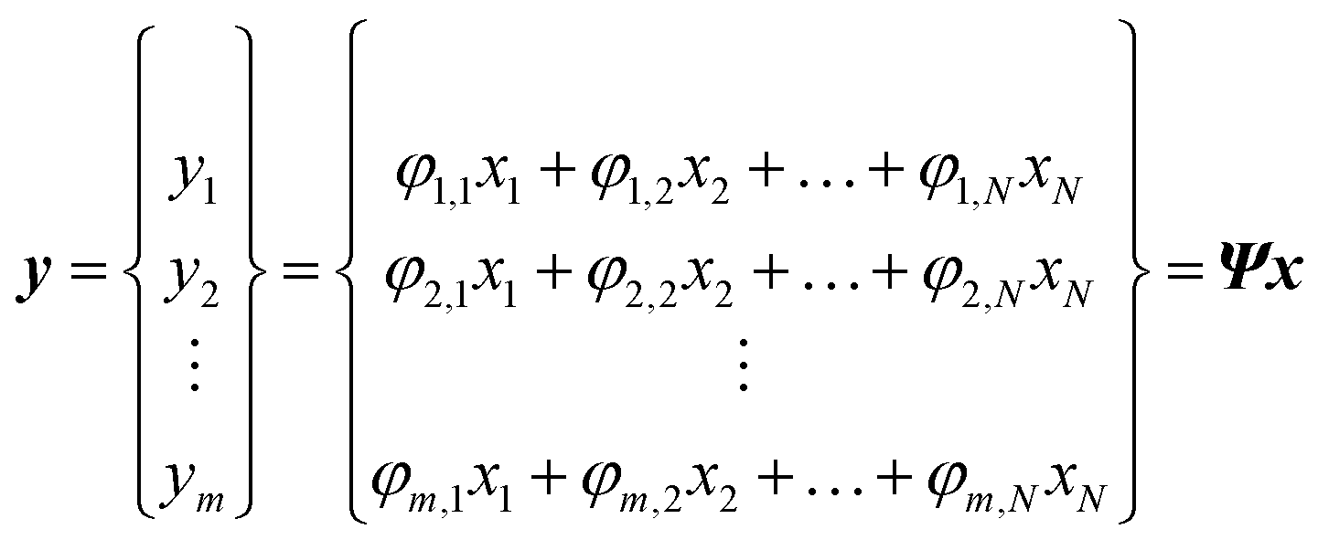 | (1) |
![[thin space (1/6-em)]](https://www.rsc.org/images/entities/char_2009.gif) log(N/K)),39 and Ψ and Φ must be incoherent to satisfy the restricted isometry property (RIP).40 These advanced algorithms can accelerate the whole process of perovskite SPI imaging.
log(N/K)),39 and Ψ and Φ must be incoherent to satisfy the restricted isometry property (RIP).40 These advanced algorithms can accelerate the whole process of perovskite SPI imaging.
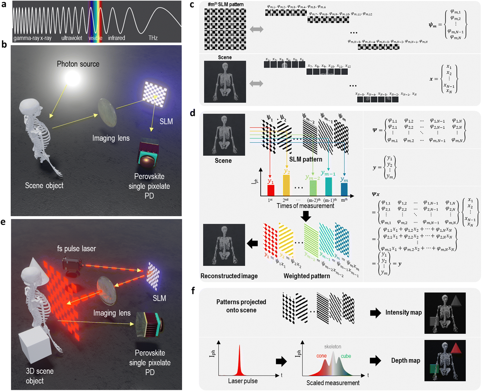 | ||
| Fig. 1 Fundamentals of perovskite SPI. (a) Schematic of electromagnetic waves of different wavelength regions, covering gamma ray, X-ray, UV-Vis-NIR, and THz regions. (b) A typical SPI setup, usually termed as a “structured” setup. A light source (or arbitrary wavelengths) illuminates onto a scene object, and the reflected light is focused by an imaging lens onto a spatial light modulator (SLM), where a sequence of binary patterns is incorporated within the SLM to pattern the light to be further detected by the perovskite single pixel photodetector (PD). It should be noted that the perovskite PD simply records an overall photocurrent or photovoltage during each measurement. And for M measurements, a series of record electrical signals with M numbers are sequentially obtained by the PD. (c) The SLM can have different patterns for each measurement. For example, at the Mth measurement, the SLM with N pixels can have a vector of ψm, which is mathematically expressed here. Similarly, when projected to this SLM, the light reflected from the scene object can be pixelated into N elements, with the scene being expressed by a vector of x, which is mathematically expressed here as well. (d) Schematic showing how each measurement using differently patterned SLM to render different electrical signals (e.g., Iph) recorded by the detector, and how these two sets of matrices can be used to calculate the scene vector x. (e) A deviated SPI setup with a time-of-flight attribute. By replacing the continuous wavelength light source with a pulse laser source, the pulse laser can incident to the SLM first for generating a transient light pattern onto the scene object (via a lens). The reflected pattern light (pulse laser light) off the object is detected by the single-pixel sensor. Due to the distance difference in the optical pathways, the temporal resolution corresponding to the 3D geometry of the scene object is encoded within the electrical signal of the photodetector, providing a measure of the distance the light has traveled thereby revealing the depth of the scene. (f) As with the structured detection approach, the sequence of projected patterns and their corresponding intensity measurements enable image reconstruction. When using a pulsed laser, the time-of-flight information from the broadened backscattered light pulse additionally allows for the creation of a depth map of the scene. Fig. 1b–f are adapted with permission from ref. 31, copyright © 2020 Optical Society of America under the terms of the OSA Open Access Publishing Agreement. | ||
In contrast to the basic setup shown in Fig. 1e for single pixel imaging, deviations such as the “structured illumination” type,41 where a modulator projects patterns onto a scene and the detector captures back-scattered intensities. These systems can be further advanced by incorporating a pulsed laser, which provides time-of-flight data, thereby enabling the measurement of scene depth.42 As demonstrated in Fig. 1f, analyzing successive signal peaks allows for the determination of an object's spatial arrangement within the scene, facilitating the creation of a depth map. For instance, the positioning of a cone in front of a skeleton and a cube behind it can be discerned through this method. Additionally, for advanced single-pixel imaging, various applications have been proposed across different fields, including traditional 2D visible light imaging,43 three-dimensional imaging,44 Lidar integration,45 and terahertz imaging.46 Moreover, the integration of single-pixel camera technology with other advanced techniques may lead to breakthroughs in imaging clarity, resolution, and speed, potentially transforming practices in medical diagnostics and research. For example, deep learning can aid in more accurately reconstructing images from sparse data, improving noise reduction, and increasing the efficiency of the imaging process. This synergy between advanced machine learning techniques and single-pixel imaging technology could pave the way for innovative applications in fields ranging from remote sensing to security surveillance, where image clarity and processing speed are crucial.
3. Spectral breakthrough by perovskite
Imaging techniques regardless of multiple pixelate imaging algorithms or single pixelate imaging, one core building block is the photodetectors, basically responsible for converting light information into electrical signal, which are crucial in various optoelectronic applications across civil and military sectors. These devices fundamentally depend on semiconducting materials like Si, Ge, PbX (X = S, Se), CdX (X = S, Se, Te), GaN, SiC, AlGaN, etc., with specific and fixed components that offer limited space to further modulate the delicate properties. However, the burgeoning demand for photodetectors with specialized functionalities, capable of responding to photons across a broad energy spectrum from X-rays to the near-infrared range, necessitates the development of semiconductors with precisely engineered bandgaps that is crucial for enabling sensitivity to specific photon energy ranges. Lead halide perovskites have emerged as a candidate material class, not only due to their wide spectral detection capability but also distinguished by their flexible compositions and remarkable photophysical properties, including high light absorption coefficient α (from 103 cm−1 to more than 105 cm−1),47 balanced ambipolar charge mobility,48 extended charge carrier diffusion length (175 μm),49,50 and easily tunable bandgap (1.88 to 3.03 eV),51–53 with versatile synthetic routes (from solution processing to all-solid and vapor processing).54 Focused on photodetectors, perovskites have shown considerable progresses, demonstrating highly desirable attributes such as exceptional responsivity (R) exceeding 109 AW−1, specific detectivity (D*) over 1016 Jones, and the fastest response time about 1 ns,55–58etc., for visible photodetection, sensitivity up to 80 μC mGyair−1 cm−3 for X-ray detector based on MAPbBr3 perovskite,59 and a detection limit of 13 nGyair s−1 from a CsPbBr3 perovskite material.60 Specifically, Fig. 2a and b18,61–79 summarize representative perovskite materials for full electromagnetic wave range detection. Simply by chemically engineering the composition, perovskite can be manifested into various crystal structures, responsive in different spectral regions (Fig. 2c). Moreover, by rationally designing the device configurations, various photonic detectors based on thin film, bulk crystal, and single crystal perovskites have been developed (Fig. 2d).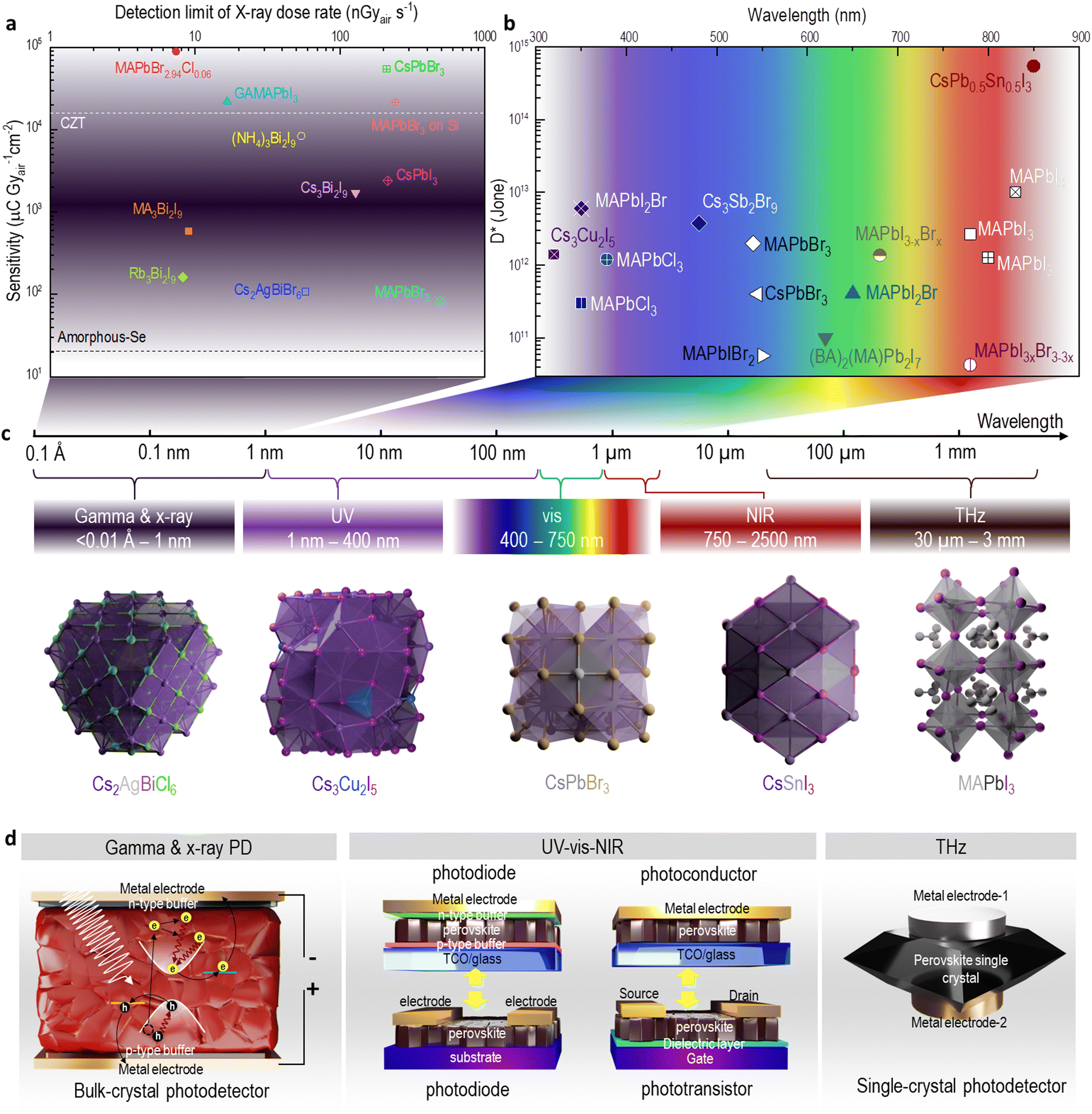 | ||
| Fig. 2 Perovskite SPI photodetector with a broad spectral response. (a) Exemplified perovskite X-ray photodetector using different perovskites showing various sensitivity and detection limit values with comparison to cadmium zinc telluride (CZT) and amorphous selenium. Data are collected from various reports,61–63 adapted with permission from ref.61. (b) Example perovskite photodetectors using different perovskites showing the specific detectivity in the spectral range of 300 to 900 nm. Data are collected from various reports.18,64–79 (c) Representative perovskite compositions used for photodetection at different regions of electromagnetic wave, covering regions from gamma and X-ray (<0.01 Å to 1 nm), UV (1–400 nm), visible (400–750 nm), NIR (750–2500 nm), and THz (30 μm to 3 mm). (d) Representative perovskite-based photodetector devices. For gamma and X-ray, usually a thick perovskite sample (either thick films, or multi-crystalline packs, or single crystals) is sandwiched between electrically asymmetric contacts. The high-energy radiation incident into the perovskite to ionize electrons to the vacuum level which can proceed in multiple ways to generate excited electrons. The excited electrons can be extracted at the cathode contact if the internal electric field is strong enough to drive the electrons to the cathode sides. A similar process is present at the anode. For UV-vis-NIR, there are four types of device geometry, which can be classified into two categories in terms of vertical or lateral configurations. For the THz, typically a perovskite single crystal is sandwiched between two metallic contacts. | ||
3.1. High-energy region
Halide perovskites stand out as promising semiconductors with unique characteristics for high-energy electromagnetic radiation detection. Their high atomic numbers and effective radiation absorption cross-section, combined with superior semiconductor properties, make them ideal for efficient and high-resolution radiation detection across various high-energy domains (e.g., record-breaking sensitivities in detecting a wide range of radiations, including X-ray,80,81 γ-rays,82–85 and even alpha particles,86,87 beta particles,88 and neutrons89,90). The predominant technologies employed for radiation detection are categorized into two types: indirect-conversion detectors (known as scintillators), and direct-conversion detectors (commonly referred to as solid-state detectors). Of particular significance are direct-conversion detectors that have the capability to directly transform high energy rays into electrical signals, which are of practical significance due to their operation at room temperature, portability, cost-effectiveness, and notably, high sensitivity and energy resolution.21For high-energy SPI, in principle one crucial precondition for reducing the measurement times (M) is to minimize the noise influence (i.e., to maximize the SNR or to improve the sensitivity of the detector). For a perovskite high-energy detector, beyond the material optimization such as utilization of single crystals, the device structural optimization plays a critical role as well. For example, the p–i–n device structure, fundamental in high-performance solid-state detectors, incorporates an intrinsic perovskite crystal sandwiched between p- and n-type contacts (Fig. 2d). And electron or hole transport (buffer) layers are inserted between the perovskite and contacts to reduce dark leakage current. Considering the radiation attenuation length, higher energy radiations (e.g., γ-rays of 100 keV to 10 MeV) require thicker perovskites exceeding 1 mm which pose a challenge for charge carriers to drift towards corresponding electrodes over such as long distance by knowing even the record carrier diffusion length in perovskite is about 175 μm. In these higher energy scenarios, ensuring a high mobility-lifetime (μ − τ) product is key for effective charge carrier movement to the contacts. On the other hand, accurate γ-ray energy calibration demands the construction of the full spectrum, identifying elements like the Compton edge and photoelectric peak, and capturing varying signal strengths from different energy interactions. For example, in a simulated γ-ray spectrum from a 137Cs source, a 1% energy resolution distinctly resolves the photoelectric peak, the lead escape peak, and the Compton edge. However, at lower resolutions (>7%), these features start to blend, reducing clarity. To address this, a high electric field is typically applied to the detector to swiftly drive all charge carriers to the electrodes within a brief time frame (ranging from microseconds to milliseconds), ensuring that all pertinent information is efficiently collected. Nevertheless, applying a high electric field also increases the dark current and speeds up ion migration. This results in additional noise and a reduction in spectral information. Thus, it becomes essential to optimize the quality of perovskite materials for high dark resistivity and to carefully design the device structure. This approach balances signal maximization and dark current minimization, crucial for effective and accurate high-energy γ-ray detection.
To date, as seen in Fig. 2a, perovskites such as MAPbBr2.94Cl0.06 exhibit a sensitivity approaching 105 μC Gyair cm−2, which is significantly higher than the state-of-the-art CZT (1600 μC Gyair cm−2).51 The efficiency of SPI in high-energy applications using perovskites can be significantly enhanced by higher sensitivity and reduced noise. In the context of high-energy SPI, similar systems to those illustrated in the “structured detection setup” and “structured illumination with time-of-flight” (as shown in Fig. 1b and e, respectively) can be applied. These systems necessitate optical pathways that are compatible with high-energy radiation, such as X-rays. Additionally, for applications like time-of-flight imaging, femtosecond pulsed high-energy radiation is required. In both cases, whether it involves patterning the reflected X-rays from the object scene or modulating the incident X-ray source, the use of an X-ray spatial light modulator (X-ray SLM) is crucial. Regular SLMs, commonly used in the visible light spectrum, are not directly applicable for manipulating X-ray beams due to the fundamental differences in how X-rays interact with matter compared to visible light. Unlike visible light, which is modulated through amplitude, phase, or polarization alterations by materials engineered for these purposes, X-rays predominantly interact via photoelectric absorption, Compton scattering, and pair production. Materials effective in manipulating visible light within regular SLMs are typically transparent to the higher energy levels of X-rays, rendering them incapable of similar modulatory effects. Creating a dynamic modulator for X-ray is challenging, necessitating materials with high atomic numbers for significant X-ray absorption and the capability for controlled, microscale modulation. Innovative approaches, like those pioneered by Sakdinawat et al.,91 utilize phase change materials such as Ge2Sb2Te5 (GST), which exhibit varying X-ray scattering properties in different physical states. In its crystalline state, GST is denser than in its amorphous form, allowing for the creation of contrast in charge density. This difference enables controlled constructive interference of X-rays at specific angles, achieved by laser-patterned imprints on the GST thin film. By patterning GST bands and zones in varying phases, reflective X-ray optics like gratings and zone plates can be fabricated. A reflective X-ray SLM thus comprises a phase change material film on silicon SLM, with switchable gratings or off-axis zone plates between active and inactive states. This technique marks a significant departure from traditional SLM methods, representing a specialized adaptation tailored for X-ray applications.
In the scenarios of “structured illumination with time-of-flight” for 3D imaging using high-energy radiation, specialized tools are indispensable. This includes not only the aforementioned X-ray SLM but also the availability of femtosecond pulse lasers capable of emitting high-energy radiative rays. Femtosecond pulse X-ray lasers are a crucial innovation in laser technology and photonics, capable of generating X-ray pulses in the femtosecond range. A prime example of this technology is the X-ray Free Electron Laser (XFEL) that are designed to produce extremely short (from a few to 100 fs)92 and intense X-ray pulses (intensities 108–1010 times greater than normal devices).93 Globally, leading XFEL facilities like the European XFEL, the Linac Coherent Light Source (LCLS) in the United States, and the SACLA facility in Japan are at the forefront of these advancements. By providing access to ultrafast timescales previously beyond the reach of conventional methodologies, these facilities are crucial for structured illumination and time-of-flight 3D imaging of perovskite SPI with high-energy radiation.
3.2. UV-Vis-NIR region
The compositional engineering of halide perovskites allows for modulation of their bandgaps, ranging from 1.24 eV to over 3.55 eV,94 corresponding to absorption edges from 1 μm to 350 nm, making them highly adaptable for various photodetector applications, including ultraviolet photodetectors (UV-PDs) towards near-infrared photodetectors (NIR-PDs). Traditional wide-bandgap inorganic semiconductors such as ZnO, Ga2O3, GaN, MgxZn1–xO, and other III–V compounds have made significant advancements in UV-PDs,95,96 demonstrating superior performance over conventional silicon-based detectors. Despite their advantages, these materials face practical limitations including challenges in material performance, high production costs, compositional fluctuations, phase separation during fabrication, complex device configurations, and high operating voltages. Halide perovskites, however, emerge as compelling alternatives for UV detection due to their remarkable properties such as large light absorption coefficients, high carrier mobility, long carrier lifetimes, low manufacturing costs, and enhanced stability. Furthermore, most inorganic semiconductors can only be grown on rigid substrates, significantly limiting their application in flexible and large-area scenarios. However, due to their simple solution preparation technology and the crystalline properties of their soft lattice, perovskite semiconductor photodetectors can be fabricated on flexible substrates.97 Notably, the light absorption characteristics of inorganic semiconductors are determined by the inherent properties of the materials themselves, necessitating the selection of specific inorganic materials to achieve optical detection across different wavelength bands. In contrast, halide perovskites offer tunable absorption and emission bands through precise compositional manipulation, allowing for customizable optical detection capabilities.98 These attributes render perovskites promising for meeting the complex requirements of single-pixel imaging. For example, all-inorganic perovskite CsPbCl3 distinguished by its exceptional ambient stability, temperature tolerance, and a wide bandgap of approximately 2.9 eV, has been proposed for UV-PD applications due to its selective sensitivity to UV signals. To further enhance the performance, there is a growing interest in single-crystal perovskites which eliminates inference of charge carrier scattering at the grain boundary. A notable example is the work by Duan et al.,99 who synthesized monocrystalline CsPbCl3 for ultra-stable and sensitive UV photodetectors. Their findings reported record figures of merit, including an ultralow dark current of 7.18 pA, an ON/OFF ratio of approximately 5.22 × 10⁵, and an external quantum efficiency of 10867%. These developments reveal the growing potential of perovskite-based materials in revolutionizing the field of UV photodetection.
In the visible range, silicon-based photodetectors, such as those in CMOS and CCD camera sensors, are prevalent in commercial and military applications. At the material level, silicon sensors often struggle with noise and limited dynamic range, impacting the ability to capture high-contrast images or perform well under low-light conditions. For example, CCD sensors can exhibit higher noise levels up to 15–20 electrons per pixel, affecting image clarity. Moreover, CCDs typically have slower readout speeds and higher power consumption, which can be limiting for high-speed imaging or applications requiring energy efficiency. Si-based CCD and CMOS sensors, integral to commercial camera imaging, necessitate intricate micro-processing for integrating sensing, memory, and control circuits at a micrometer scale within a compact imaging chip. This demands precise processing to ensure functionality and compatibility of components. However, as technology approaches the miniaturization limits prescribed by Moore's Law, maintaining progress in silicon-based sensors becomes increasingly challenging and costly, especially as further miniaturization is essential for improving resolution and sensitivity. These manufacturing complexities highlight the need for alternative materials and technologies that offer simpler fabrication methods, flexible device architectures, and a wider spectral response. This makes them viable and cost-effective alternatives to traditional silicon-based photodetectors. Emerging materials like organics, 2D, and quantum materials open new avenues, but their advancement is limited by inherent poor charge-carrier mobility, which restricts detection performance. Perovskite materials, on the other hand, present a solution to these challenges at the material level. However, their limited compatibility with nanotechnology, such as lithography, poses a significant barrier to directly integrating perovskite photonic sensing materials with existing CMOS and CCD manufacturing techniques.
To fully harness the superior material properties of perovskites while circumventing the challenges of multi-pixel microarray manufacturing, alternative imaging methods are required. One such method is single-pixel imaging, which can utilize the advantages of perovskites without the complexities of existing multipixel-based device architecture. Specifically, the manufacturing of multi-pixel microarrays, composed of numerous small pixels that can function as photodetectors or other types of sensors, presents several key limitations: (1) pixel size constraints: the manufacturing process is limited by the constraints of photolithography and other nanofabrication techniques, restricting the minimum pixel size. While smaller pixels offer higher resolution, they also increase manufacturing complexity and cost. (2) Precision in pixel manufacturing: the process used to manufacture pixelated arrays must precisely control the size and position of each pixel to ensure the array's performance and uniformity. High-precision manufacturing processes, such as CMOS technology, can be utilized for large-scale pixel arrays; however, these processes are often costly. (3) Power consumption: each pixel in a pixelated array may require its own signal processing circuitry, leading to increased overall power consumption. (4) Complex manufacturing and assembly: the manufacturing and assembly of pixelated arrays are complex processes involving multiple steps and highly specialized equipment. To overcome these limitations, new technologies aim to improve pixel designs and enhance device performance while reducing costs and power consumption. The manufacturing of perovskite-based SPI does not require high-precision micro/nano-sized components. Without complex arrays, the device design involves a simple stacking of functional layers perpendicular to the direction of incident light.4 Compared to CMOS devices, the volume of data in photoelectric signal processing is reduced by orders of magnitude in perovskite-based SPI systems. This approach represents a promising direction for the future of photodetection, offering a balance between material excellence and manufacturing feasibility. For instance, Mai and Wang et al.100,101 have demonstrated the potential of perovskite-based SPI by using three distinct perovskite types, each sensitive to red, green, or blue light. When combined with the Fourier imaging algorithm for SPI, they effectively generated color images from monochromatic data, especially when the RGB photodetectors are exposed to low light levels at 20 μW cm−2. Additionally, integrating a white photodetector and utilizing a simple overlay method for color/white image fusion, they achieved color imaging capabilities even under weaker illumination around 5.4 μW cm−2. This research heralds a new era in exploring novel materials and methods for the development of advanced, high-performance imaging technologies. In a similar vein, Wei et al.102 employed a high-performance perovskite hemispherical photodetector with an exceptionally high external quantum efficiency (around 1000%) and low noise level (10−13 A Hz−0.5). They utilized a neural network fitting (NNF) assisted machine learning algorithm to correlate the differential current signal with various applied biases for color recognition in SPI. This approach enabled the development of dual frameworks that can dynamically track an object's trajectory in 3D space and incorporate a color classification functionality on a 2D plane, representing a significant stride forward in photodetection technology and showcasing the potential of perovskites in cutting-edge imaging advancements.
3.3. THz region
Terahertz (THz) imaging, transitioning from research labs to commercial use, is an exciting field with growing interest. Its ability to see through nonpolar liquids and non-conductive materials makes it ideal for non-invasive inspections in various applications, including examining artworks, electronic circuits, space shuttle panels, and carbon-fiber composites,103,104 as well as the monitoring of picosecond processes in semiconductors,105 pharmaceutical quality control (by observing and controlling fundamental material resonances such as phonons, molecular rotations, and spin precessions),106 and explosive detection. In biomedicine, its non-ionizing nature and sensitivity to water content offer label-free diagnostics for diseases like cancer and diabetic foot syndrome, altering water content,107,108 and intense THz radiation has potential applications in DNA repair.109 To date, the commercial viability of THz imaging techniques is hindered by several significant drawbacks. First, materials suitable for efficient THz detection are scarce, leading to detector arrays that either operate in narrow bandwidths or require cryogenic temperatures for sensitive detection.110 Microbolometer arrays, although capable of operating at room temperature with wide bandwidths,111 do not offer the necessary picosecond temporal resolution and depend on frequency-selective sources for frequency resolution. This leads to issues in applications where time gated detection is used, such as analyzing depth-dependent layers in artwork.104 An alternative is projecting a THz image onto an electro-optic crystal (analogous to the “scintillator” working principle in the aforementioned high-energy section) and mapping the THz field with visible light CCD arrays,112,113 which maintains temporal resolution but requires a large, expensive regen-amplified Ti-Sapphire laser system, hindering widespread adoption. Additionally, far-field imaging methods generally fail to resolve details smaller than approximately 500 μm due to the inherent wavelengths of THz radiation. Furthermore, near-field techniques like AFM-tips,112,114,115 THz-fiber probes,104 or air-plasma for sub-wavelength imaging113 can offer finer details, but they are complex and require specialized setups, making them impractical for mainstream commercial use. These challenges collectively contribute to the limited adoption of THz imaging technology outside research settings, despite its potential for a wide range of applications.Single pixel imaging, when combined with advanced THz sensing materials such as perovskites, significantly improves system robustness while simplifying design and reducing costs. Recent experiments have showcased the remarkable potential of halide perovskites in THz optoelectronics.116–121 For example, most of these perovskites, when excited with a femtosecond laser, can generate ultrafast photocurrents and emit THz pulses. The recent breakthrough in perovskite-based THz modulators marks a journey from theoretical development to practical application, even reaching early stages of commercialization.122 Utilizing a compressive imaging approach, along with intelligent deep learning algorithms, enhances the potential of advanced perovskite-based THz single-pixel detectors for fast and cost-effective THz imaging. This combination is particularly promising because it aligns well with single-element detectors like photoconductive antennas that are capable of accurately measuring the amplitude and phase of a THz pulse with an impressive temporal resolution of 100 femtoseconds.
The detection of THz radiation remains a significant challenge,123 despite advancements in narrow bandgap semiconductors like HgCdTe,124 quantum wells such as GaAs/InGaAs,125 and even gapless semiconductors like graphene and Dirac semimetals.126 The difficulty primarily arises from the low photon energy of THz radiation (0.41 to 41 meV), which is close to the thermal energy at room temperature (25 meV). This proximity necessitates the use of cryogenic cooling systems in conventional photoelectric detection methods to suppress the dark current and maintain temperatures below 4 K, making these systems bulky and limiting their widespread application. To address these challenges, room-temperature THz detection devices have been developed using nonlinear meta-surfaces and antennas,127–129 however they require complex fabrication processes due to specific architectural needs, such as logarithmic-periodic or multi-resonant structures, to enhance THz signal resonance. An effective alternative strategy involves exploiting the thermoelectric effects (bolometric, Seebeck, and pyroelectric effects), which can directly convert THz radiation into a detectable DC signal at room temperature. Materials like graphene,130 TaAs,131 and WTe2132 have shown promise in this approach but technically limited by their synthesis into acceptable wafer sizes. Halide perovskites offer a promising solution to these limitations, with properties conducive to piezoelectric, ferroelectric, and attributes of ultralow thermal conductivity (e.g., 0.13 W m−1 s−1 from the Cs1.9Sn1.025I6),133 negative temperature coefficient of resistance, and a notable Seebeck effect (e.g., MAPbI3 9 × 10⁴ μV K−1vs. typical thermoelectric materials of bismuth telluride alloy of ∼200 μV K−1),133 making them attractive candidates for thermoelectric THz detection devices. Recent innovations, such as those by Yao et al.,134 have demonstrated the potential of HPs in THz detection at room temperature by observing a significant increase in current due to bolometric and photo-thermoelectric effects under THz irradiation in MAPbI3 polycrystalline films. Xu et al.123 advanced THz detection by incorporating an anti-reflection 2D perovskite layer on MAPbI3 single crystals, achieving enhanced room-temperature THz detection, which yielded a remarkable responsivity of 88.8 μA W−1 at 0.1 THz with an electric field of 60 V cm−1, and a notably low noise equivalent power (NEP) of less than 2.16 × 10⁻⁹ W Hz−1/2. This performance, highlighted by a specific detectivity (D*) of 1.5 × 10⁸ Jones, surpasses many graphene-based devices, marking a significant breakthrough in THz detection technology and paving the way for advanced imaging and sensing applications. Makarov et al.24 developed the single-crystalline MAPbI3 and MAPbBr3-based THz photoconductive detectors with a core detection mechanism of capturing the oscillations of electric fields in the time domain. This is achieved by measuring the photocurrent that emerges in the optically excited perovskites when they are subjected to THz pulse exposure. Remarkably, when excited with 40 fs pulses at a wavelength of 400 nm, these perovskite-based detectors displayed detectivity in the 0.1–2 THz range, which is on par with conventional detectors that rely on electro-optical sampling in nonlinear crystals. These findings are crucial as they not only enhance our understanding of perovskite-based optoelectronics but also open up new avenues for the development of efficient and cost-effective hybrid perovskite-based THz devices.
The future of SPI with perovskite-based THz detectors is brimming with potential, thanks in large part to the distinct qualities of perovskites and the inherent strengths of SPI methods. Besides the crucial development of SLMs for THz applications, there are several promising pathways to expedite research and development in this technology: (1) enhanced material properties: future research may focus on optimizing the perovskite material properties specifically for THz detection. This includes enhancing carrier mobility, reducing trap densities, and improving stability under THz radiation. Tailoring the composition of perovskites to optimize their response in the THz range could lead to more sensitive and efficient detectors. (2) Integration with advanced algorithms: SPI relies heavily on computational methods for image reconstruction. Integrating perovskite THz detectors with advanced algorithms, particularly with machine learning and deep learning neuromorphic, could significantly improve image reconstruction quality. These algorithms can be trained to effectively handle the sparse data from single-pixel setups, enhancing the overall resolution and image quality. (3) Hybrid detection systems: combining perovskite THz detectors with other types of sensors could lead to hybrid systems capable of multi-modal imaging. This approach can harness the strengths of different sensing technologies, offering more comprehensive data and better imaging capabilities. (4) Dynamic range and sensitivity improvement: research could focus on increasing the dynamic range and sensitivity of perovskite THz detectors. This would involve not only material improvements but also advancements in the design of the device and SPI system setup, such as optimizing the modulation patterns used for imaging and enhancing the signal-to-noise ratio. (5) Compact and flexible systems: the development of compact and flexible perovskite THz detectors would be highly beneficial for practical applications. Research into thin-film perovskites and flexible substrates could lead to portable and versatile THz imaging systems suitable for a wide range of applications, from medical imaging to security screening. (6) Real-time imaging capabilities: currently, one of the limitations of SPI is the speed of image acquisition. Future research could focus on increasing the speed of both the detection and the computational processes to enable real-time THz imaging, which would be a significant breakthrough for many applications. (7) Addressing stability and durability: perovskites are known for issues related to stability, especially under varying environmental conditions. Research into making these materials more robust and durable would greatly enhance the practicality of perovskite-based THz detectors. (8) Customizable and scalable fabrication: exploring scalable and cost-effective fabrication methods for perovskite THz detectors would be essential for commercial viability. This includes methods that are compatible with existing manufacturing technologies and allow for customization based on specific application needs. In summary, the future research on perovskite-based SPI for THz detection is rich with opportunities. By addressing current limitations and harnessing the full potential of perovskites, these systems could revolutionize THz imaging and open new frontiers in various scientific and industrial fields.
4. Challenges and strategies of perovskite-based SPI device realization
4.1. Perovskite materials stability
One of the major challenges in the realization of perovskite-based SPI devices is the instability of perovskite materials. Despite their excellent performance, perovskite materials often suffer from issues related to environmental degradation, which significantly impacts their long-term reliability and functionality. We believe that addressing the stability of perovskite materials is crucial and requires a comprehensive approach that spans various aspects of physical and chemical technologies. Notable progress has been reported in recent years concerning stability improvements. Although our primary focus is on the engineering applications and innovative developments of perovskite-based SPI systems, we outline several simplified material stability strategies here.For unpackaged devices, the inherent instability of halide perovskite materials can be addressed through the following approaches: Adjusting the composition of perovskites can enhance their stability by altering lattice parameters and bond environments to maintain the original 3D perovskite structure. For instance, El-Mellouhi et al. demonstrated that substituting iodide with the smaller bromide ion reduces the perovskite lattice parameter, resulting in a more stable cubic perovskite, likely due to strengthened organic cation-lead halide bonding.135,136 Additionally, Saidaminov et al. detailed that introducing cadmium as a B-site dopant in the perovskite lattice relaxes local strain and suppresses vacancy formation, thereby significantly increasing stability in ambient air.137 Certain organic groups can form chemical or coordination bonds with perovskite materials on the surface, inducing stress on the lattice surface and hindering phase transitions through spatial effects. These organic groups can also serve a hydrophobic protective role. For example, Wang et al. added hydroiodic acid and phenylammonium iodide (PEAI) to the precursor solution. PEAI aids nucleation, optimizing crystallization, and impeding phase transitions through spatial effects. After being exposed to air for two months, efficiency decreased by only 8%.138 Applying a protective layer, such as a metal oxide or a second perovskite layer, can shield perovskites from environmental factors contributing to instability. For instance, combining 2D and 3D inorganic perovskite structures has shown excellent stability. This approach involves secondary growth of a planar perovskite layer on the surface of a 3D inorganic perovskite structure, leveraging the high surface energy of the 2D perovskite layer to eliminate interface defects and passivate the surface effectively.139 Additionally, Wang et al. coated perovskite thin films with a layer of trimethyl phenylammonium bromide (PTABr). Due to the excellent hydrophobicity of PTABr, the film maintained its black appearance at a relative humidity of 85%, demonstrating outstanding humidity stability.140 These strategies highlight ongoing efforts to improve the stability and practical applicability of perovskite materials in optoelectronic devices, thus also has the potential to address one of the critical challenges in the realization of perovskite-based SPI systems.
4.2. Preparation methods
Perovskite-based SPI devices necessitate the precise realization of multilayer thin films, with stringent control over layer thickness, composition, and interfacial quality. One of the primary challenges in this context is achieving high-quality multilayer thin films and ensuring appropriate contact between single crystals using solution-based techniques alone. The difficulty in fabricating multilayer thin films via solution methods arises from the need to maintain consistent chemical processes during nucleation and crystallization, which are influenced by various physical changes. Several strategies can help overcome these challenges: Post-deposition annealing can enhance crystallinity, reduce organic content, and improve the interfacial quality between layers, thereby producing higher quality film integrations.141 Techniques such as doctor blading, slot-die coating, spray coating, inkjet printing, and soft-cover deposition provide better control over film thickness and uniformity, essential for creating high-quality multilayer structures.142 An alternative deposition method such as vacuum vapor deposition143 and all-solid synthesis133 involving the dry preparation of multilayer thin films can be helpful. In a solvent-free environment, both organic and inorganic materials required for the functional layers are sublimated and deposited onto the substrate by heating through an evaporation source. The uniform conditions in the vacuum chamber facilitate easier control over the uniformity and consistency of the deposited films.For single-crystal based devices, to ensure effective contact between single crystals, utilizing interfacial layers designed to promote perovskite crystallization and enhance interlayer integration is crucial. Special perovskite inks can be used in solution techniques to improve single crystal contacts. For instance, a custom-made homogeneous ink can be employed to connect MAPbI3 perovskite single crystals. This ink is produced by dissolving perovskite precursor powders with methylamine gas and dispersing them in acetonitrile solvent. The rapid crystallization rate of this ink allows for the preparation of perovskite phases without traditional post-processing, ensuring successful contact between MAPbI3 single crystals.144
These strategies highlight ongoing efforts to address the challenges associated with multilayer thin film fabrication and single crystal contact in perovskite-based SPI devices, thereby enhancing their practical applicability and performance.
4.3. Charge transfer mechanism
The charge transfer mechanism between multilayer thin films or between single crystals is a critical factor in the performance of perovskite-based SPI devices. Efficient charge transfer is essential for optimal photoelectric conversion and overall device functionality. However, perovskite materials face several challenges in this regard, including charge recombination and poor interfacial charge transfer. Addressing these issues is crucial for optimizing device performance. Specifically, improving the quality of the interfaces between different layers or single crystals is vital for enhancing charge transfer. Strategies such as introducing buffer layers or passivation layers can reduce charge recombination at the interfaces. For instance, materials like PCBM (phenyl-C61-butyric acid methyl ester) or PTAA (poly(triarylamine)) as interfacial layers can help in passivating defects and enhancing charge transport.145 Introducing dopants or creating alloyed perovskite compositions can modify the electronic properties of the material, facilitating better charge transport. For example, adding elements such as tin or incorporating mixed halide compositions can help in tuning the bandgap and enhancing charge mobility.146 High crystallinity in perovskite films or single crystals is crucial for effective charge transfer.144 Techniques such as solvent engineering, thermal annealing, and vapor-assisted deposition can improve crystallinity and reduce defects, thereby enhancing charge transport properties. Applying surface treatments to perovskite layers can also improve charge transfer.147 Treatments with materials such as fullerene derivatives, self-assembled monolayers, or metal oxides can enhance surface passivation and reduce surface recombination, leading to better charge transport across interfaces. Employing advanced characterization techniques to study charge dynamics at the interfaces can provide insights into the charge transfer mechanisms and identify bottlenecks.148 Techniques such as transient photovoltage measurements, time-resolved photoluminescence, and impedance spectroscopy can help in understanding and optimizing charge transfer processes.By addressing these charge transfer challenges through the strategies outlined above, the performance and efficiency of perovskite-based SPI devices can be significantly enhanced, paving the way for their practical application in various optoelectronic technologies.
5. Outlook
Advantages of SPI, such as high sensitivity, flexibility in working with different wavelengths, and the ability to reconstruct images from sparse data methodologies,13,15,34–36,39 can be strategically utilized. This can lead to various prospects in different future directions, including scenarios as follows.5.1. Multi-information imaging
Multi-information imaging is proposed as a versatile tool across various fields to simultaneously collect various signal aspects of e.g., hyperspectral-, quantum-, and time-information, etc., using perovskite materials in conjunction of SPI systems. Fig. 3a illustrates a conceptual approach to multi-information imaging, employing a multispectral light source to illuminate the target. The target reflects this light, which now carries embedded bioinformation. This reflected light is spatially encoded by an SLM and subsequently captured by a series of perovskite photodetectors, each sensitive to a distinct spectral region. This setup allows each photodetector to produce an image linked to its respective wavelength, thus achieving multi-wavelength imaging in a single illumination instance.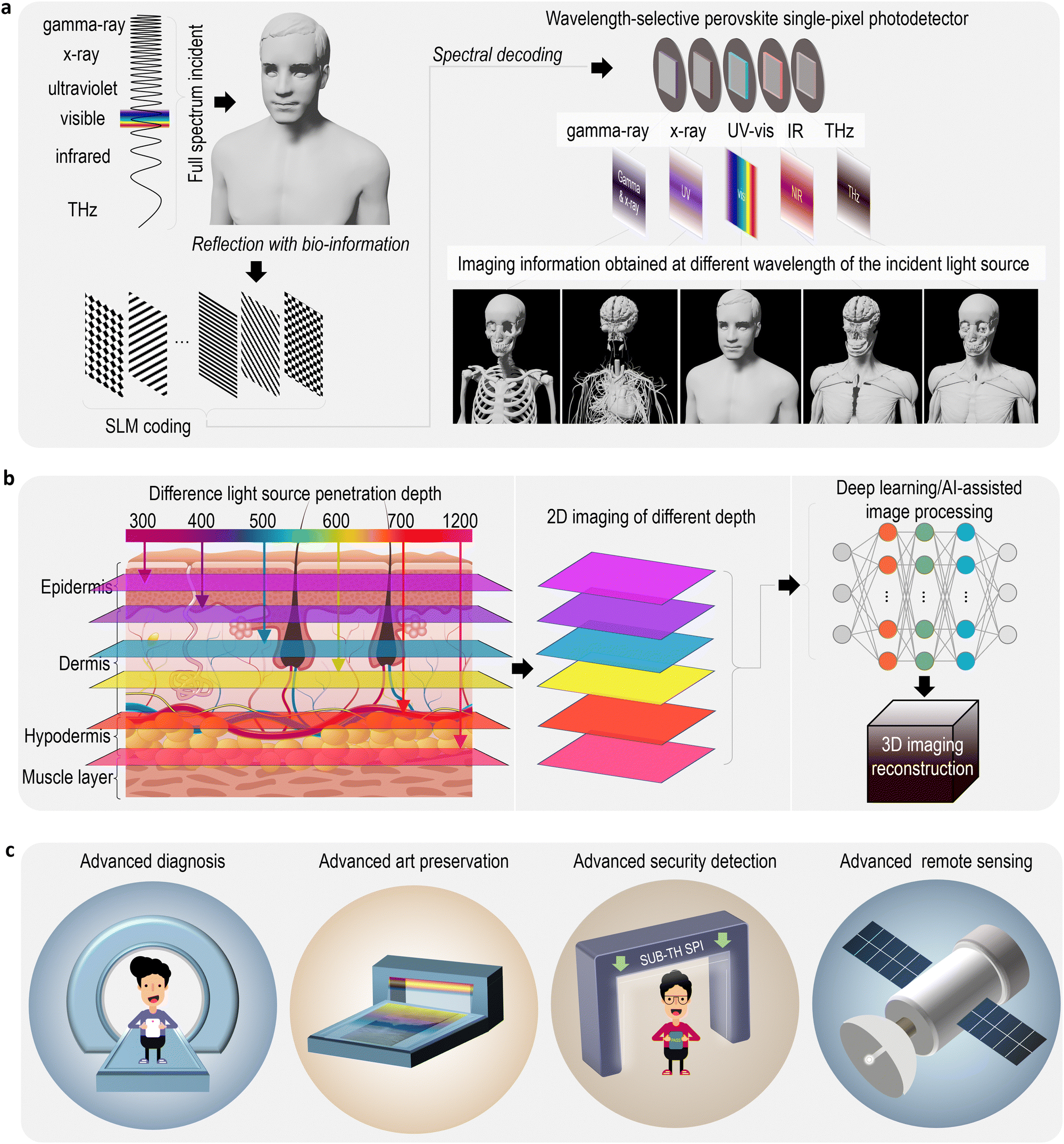 | ||
| Fig. 3 Technical further building upon perovskite SPI. (a) The proposed multi-information imaging technique is illustrated here, utilizing a multispectral light source that illuminates an object. This object reflects the light, embedding it with bioinformation. The reflected light undergoes spatial encoding via an SLM, then is captured by an array of perovskite photodetectors tuned to specific spectral regions. Each photodetector generates an image corresponding to its unique wavelength, enabling simultaneous multi-wavelength imaging from a single illumination event. (b) Multispectral 2D imaging facilitates 3D model reconstruction. Light of varying wavelengths penetrates the object (e.g., skin) to different depths, producing slice-by-slice images. These images, processed through deep learning or AI-assisted techniques, culminate in the reconstruction of a 3D model. (c) Demonstrating the versatility of perovskite SPI in advanced imaging applications: Enhanced diagnostic capabilities through noninvasive THz imaging; preservation and analysis of artwork with multispectral imaging without causing damage; heightened security measures with THz and sub-THz SPI systems capable of penetrating clothing and non-metallic objects while ensuring privacy; and improved remote sensing and astronomical observations, courtesy of the superior sensitivity and low-light performance of perovskite SPI, overcoming atmospheric interference for clearer, more detailed imagery. | ||
In environmental monitoring and climate research, perovskite-based SPI systems are invaluable due to their ability to detect a wide range of wavelengths, from ultraviolet to infrared. This broad spectral response allows for detailed analysis of environmental indicators such as vegetation health, soil moisture, air quality, and water pollution, with high sensitivity and performance under low-light conditions. For hyperspectral SPI, perovskite's broad spectral response enables each pixel in an image to capture a wide spectrum of light, allowing for detailed spectral analysis at each image point. This technology is crucial in applications like precision agriculture and art restoration, where accurate material composition and change detection are essential. Quantum imaging with SPI149–151 leverages the principles of quantum entanglement and superposition, where perovskite's sensitivity enhances image resolution and reduces noise, making it particularly useful in quantum microscopy and non-invasive medical diagnostics, where capturing minute details is critical. Overall, the integration of perovskite into SPI components across these varied applications offers a multitude of benefits, including enhanced sensitivity, compact system design, and the ability to capture a wide range of spectral and temporal information, making it a powerful tool in multi-information imaging.
5.2. Intelligent imaging
The incorporation of perovskite-based SPI is also expected to revolutionize machine vision and robotics, particularly in autonomous systems, by significantly enhancing performance under diverse environmental conditions. Perovskite materials, known for their exceptional sensitivity to a broad spectrum of wavelengths and superior narrowband photosensitivity, can lead to intelligent imaging. For example, Fig. 3b showcases how multispectral 2D imaging can be instrumental in creating 3D models. By employing light of distinct wavelengths, it is possible to penetrate an object, such as human skin, at varying depths. This process results in the generation of images that represent individual slices of the object at different depths. Subsequently, through the application of advanced deep learning or AI-assisted image processing techniques, these layered images are meticulously compiled, leading to the reconstruction of a comprehensive 3D model. This technique underscores the potential of multispectral imaging in enhancing our understanding and visualization of complex structures in a non-invasive manner.Additionally, perovskite optoelectronic materials also offer improved imaging capabilities in low-light scenarios, a critical aspect for navigation and object detection in autonomous vehicles or drones operating in dim environments. This technology also excels in imaging through obscure mediums, such as fog or smoke, providing clearer vision where traditional systems struggle, thereby enhancing safety and operational efficiency. Furthermore, the high resolution and sensitivity of perovskite-SPI systems advance object detection and classification algorithms, crucial for automated tasks in various industries. The robustness of these systems, capable of maintaining performance under extreme temperatures and varying light conditions, is particularly beneficial for outdoor robotics applications. This advancement is paving the way for more sophisticated autonomous applications, such as drones for search and rescue, precision agriculture, and environmental monitoring, where detailed and reliable imaging is paramount, demonstrating the transformative impact of perovskite-SPI in machine vision and robotics.
Scaling these systems for widespread use, while maintaining performance and cost-effectiveness, will be crucial for their adoption in various industries. Additionally, addressing power consumption is vital, as efficient energy used directly impacts the feasibility of deploying these systems in battery-operated autonomous devices. Considerations for seamless integration into existing systems will also play a pivotal role in ensuring that perovskite-SPI technology can be effectively utilized in practical applications, thereby maximizing its potential benefits.
5.3. Advanced imaging application
Incorporating perovskite materials into SPI systems can substantially advance their capabilities across various applications (Fig. 3c). For example, in medical imaging, the broad spectral response of perovskite enhances SPI's effectiveness in non-invasive procedures. This advancement allows for more detailed and safer internal body imaging using non-ionizing radiation like THz or infrared, which is crucial for diagnosing diseases early and monitoring chronic conditions without the risks associated with traditional ionizing methods. For art and cultural heritage preservation, the sensitivity of perovskite-based SPI toward a wide range of wavelengths enables a more thorough and non-destructive analysis of artworks and historical artifacts. This attribute is particularly beneficial in revealing hidden layers or details without damaging these precious items. In security applications, the use of perovskite in THz and sub-THz SPI systems significantly improves the detection capabilities. It enhances the ability to penetrate clothing and non-metallic materials while maintaining high-resolution imaging, thus ensuring safety and privacy at security checkpoints. Moreover, the high sensitivity and low-light performance of perovskite-based SPI play a critical role in remote sensing and astronomical applications. They enable the capture of clearer and more detailed images from satellites or high-altitude platforms for environmental monitoring, and in astronomy, they provide enhanced clarity in observing distant celestial bodies, overcoming challenges posed by atmospheric interference. Overall, the integration of perovskite in SPI systems across these diverse fields not only amplifies their existing functionalities but also opens new possibilities for innovation in advanced imaging technology, making SPI a more versatile and powerful tool.Future research in SPI integrated with perovskite materials offers vast potential across several promising areas. Key focuses include the development of new perovskite composites for enhanced stability and sensitivity, and the optimization of algorithms for improved image reconstruction and data processing, potentially leveraging machine learning and AI. Miniaturization and integration of SPI systems with technologies like MEMS or flexible electronics could broaden their practical applications, including in wearable tech. Advancements in quantum imaging could revolutionize resolution and sensitivity, particularly beneficial in quantum microscopy and non-invasive diagnostics. Improving the dynamic range and sensitivity of SPI systems will facilitate more effective imaging under diverse lighting conditions, while developing real-time processing capabilities is crucial for applications in autonomous vehicles and robotic surgery. Expanding the efficiency of multispectral and hyperspectral imaging could greatly benefit agriculture and environmental science. In the biomedical field, research could explore in vivo imaging for enhanced diagnostics and treatment. Enhancements in security and surveillance using SPI could focus on non-invasive, privacy-preserving technologies. Additionally, applying perovskite-SPI in environmental and climate research could lead to more extensive monitoring and understanding of ecological and atmospheric changes. This breadth of research underscores the transformative potential of perovskite-SPI in advancing imaging technology across numerous disciplines.
Author contributions
K. W. and J. Q. conceived the idea and supervised the project. K. W., X. W., and L. R. prepared the manuscript and developed the figures. H. Z. and C. W. significantly contributed to the technical discussions and edited the manuscript. All the authors actively participated in discussions and collaboratively contributed to the manuscript development. Please note that the author K.W. was in the faculty at Penn State University when the idea was constructed. During the manuscript preparation stage, K.W. took new positions at other affiliations as indicated in the author information.Data availability
No primary research results, software or code have been included and no new data were generated or analyzed as part of this review.Conflicts of interest
There are no conflicts of interest to declare.Acknowledgements
C. W. acknowledges the Key Research and Development Program of Hubei Province, China (Grant No. 2022BAA096). J. Q. acknowledges support from the National Natural Science Foundation of China (No. 12125205). X. W., L. R., H. Z. and K. W. acknowledge the support from Huanjian Laboratory.References
- B. Mandracchia, X. Hua, C. Guo, J. Son, T. Urner and S. Jia, Nat. Commun., 2020, 11, 94 CrossRef CAS PubMed.
- H. Song, S. Sasada, T. Kadoya, K. Arihiro, M. Okada, X. Xiao, T. Ishikawa, D. O’Loughlin, J. Takada and T. Kikkawa, IEEE Trans. Biomed. Eng., 2023, 1–12 Search PubMed.
- M. Sonka, H. Vaclav and R. Boyle, Image processing, analysis and machine vision, 2013 Search PubMed.
- Y. Hou, J. Li, J. Yoon, A. M. Knoepfel, D. Yang, L. Zheng, T. Ye, S. Ghosh, S. Priya and K. Wang, Sci. Adv., 2024, 9, eade2338 CrossRef.
- A. El Gamal and H. Eltoukhy, IEEE Circuits Devices Mag., 2005, 21, 6–20 CrossRef.
- J.-W. Luo, S.-S. Li, I. Sychugov, F. Pevere, J. Linnros and A. Zunger, Nat. Nanotechnol., 2017, 12, 930–932 CrossRef CAS PubMed.
- K. E. Petersen, Proc. IEEE, 1982, 70, 420–457 CAS.
- P. Sen, B. Chen, G. Garg, S. R. Marschner, M. Horowitz, M. Levoy and H. P. A. Lensch, ACM SIGGRAPH 2005 Papers, Association for Computing Machinery, New York, NY, USA, 2005, pp. 745–755 Search PubMed.
- C. M. Watts, D. Shrekenhamer, J. Montoya, G. Lipworth, J. Hunt, T. Sleasman, S. Krishna, D. R. Smith and W. J. Padilla, Nat. Photonics, 2014, 8, 605–609 CrossRef CAS.
- S. M. Hornett, R. I. Stantchev, M. Z. Vardaki, C. Beckerleg and E. Hendry, Nano Lett., 2016, 16, 7019–7024 CrossRef CAS.
- J. Greenberg, K. Krishnamurthy and D. Brady, Opt. Lett., 2014, 39, 111–114 CrossRef PubMed.
- A.-X. Zhang, Y.-H. He, L.-A. Wu, L.-M. Chen and B.-B. Wang, Optica, 2018, 5, 374–377 CrossRef CAS.
- D. L. Donoho, IEEE Trans. Inf. Theory, 2006, 52, 1289–1306 Search PubMed.
- E. J. Candes and T. Tao, IEEE Trans. Inf. Theory, 2006, 52, 5406–5425 Search PubMed.
- M. F. Duarte, M. A. Davenport, D. Takhar, J. N. Laska, T. Sun, K. F. Kelly and R. G. Baraniuk, IEEE Signal Process Mag., 2008, 25, 83–91 Search PubMed.
- O. Katz, Y. Bromberg and Y. Silberberg, Appl. Phys. Lett., 2009, 95, 131110 CrossRef.
- C. G. Graff and E. Y. Sidky, Appl. Opt., 2015, 54, C23–C44 CrossRef PubMed.
- J. Li, J. Wang, J. Ma, H. Shen, L. Li, X. Duan and D. Li, Nat. Commun., 2019, 10, 806 CrossRef.
- M. Zhang, F. Zhang, Y. Wang, L. Zhu, Y. Hu, Z. Lou, Y. Hou and F. Teng, Sci. Rep., 2018, 8, 11157 CrossRef PubMed.
- C. Motta, F. El-Mellouhi and S. Sanvito, Sci. Rep., 2015, 5, 12746 CrossRef CAS PubMed.
- F. Liu, R. Wu, J. Wei, W. Nie, A. D. Mohite, S. Brovelli, L. Manna and H. Li, ACS Energy Lett., 2022, 7, 1066–1085 CrossRef CAS.
- Y. Su, W. Ma and Y. (Michael) Yang, J. Semicond., 2020, 41, 051204 CrossRef CAS.
- K. Sakhatskyi, B. Turedi, G. J. Matt, E. Wu, A. Sakhatska, V. Bartosh, M. N. Lintangpradipto, R. Naphade, I. Shorubalko, O. F. Mohammed, S. Yakunin, O. M. Bakr and M. V. Kovalenko, Nat. Photonics, 2023, 17, 510–517 CrossRef CAS.
- P. A. Obraztsov, P. A. Chizhov, D. S. Gets, V. V. Bukin, O. I. Semenova and S. V. Makarov, ACS Photonics, 2022, 9, 1663–1670 CrossRef CAS.
- K. Wang, D. Yang, C. Wu, M. Sanghadasa and S. Priya, Prog. Mater. Sci., 2019, 106, 100580 CrossRef CAS.
- M. I. Saidaminov, I. Spanopoulos, J. Abed, W. Ke, J. Wicks, M. G. Kanatzidis and E. H. Sargent, ACS Energy Lett., 2020, 5, 1153–1155 CrossRef CAS.
- P. Zhang, G. Yang, F. Li, J. Shi and H. Zhong, Nat. Commun., 2022, 13, 6713 CrossRef CAS.
- B. Jeong, H. Han and C. Park, Adv. Mater., 2020, 32, 2000597 CrossRef CAS PubMed.
- Z. Zhang, X. Ma and J. Zhong, Nat. Commun., 2015, 6, 6225 CrossRef CAS.
- M. P. Edgar, G. M. Gibson and M. J. Padgett, Nat. Photonics, 2019, 13, 13–20 CrossRef CAS.
- G. M. Gibson, S. D. Johnson and M. J. Padgett, Opt. Express, 2020, 28, 28190–28208 CrossRef.
- W. K. Pratt, J. Kane and H. C. Andrews, Proc. IEEE, 1969, 57, 58–68 Search PubMed.
- N. J. A. Sloane and M. Harwit, Appl. Opt., 1976, 15, 107–114 CrossRef CAS PubMed.
- R. G. Baraniuk, IEEE Signal Process Mag., 2007, 24, 118–121 Search PubMed.
- M. Rani, S. B. Dhok and R. B. Deshmukh, IEEE Access, 2018, 6, 4875–4894 Search PubMed.
- E. J. Candes and M. B. Wakin, IEEE Signal Process Mag., 2008, 25, 21–30 Search PubMed.
- G. K. Wallace, Commun. ACM, 1991, 34, 30–44 CrossRef.
- A. Skodras, C. Christopoulos and T. Ebrahimi, IEEE Signal Process Mag., 2001, 18, 36–58 CrossRef.
- M. Fornasier and H. Rauhut, Handbook of mathematical methods in imaging, 2015, pp. 187–229 Search PubMed.
- M. A. Davenport and M. B. Wakin, IEEE Trans. Inf. Theory, 2010, 56, 4395–4401 Search PubMed.
- T. Lu, Z. Qiu, Z. Zhang and J. Zhong, Opt. Lasers Eng., 2020, 134, 106301 CrossRef.
- M.-J. Sun, M. P. Edgar, G. M. Gibson, B. Sun, N. Radwell, R. Lamb and M. J. Padgett, Nat. Commun., 2016, 7, 12010 CrossRef.
- S. S. Welsh, M. P. Edgar, R. Bowman, P. Jonathan, B. Sun and M. J. Padgett, Opt. Express, 2013, 21, 23068–23074 CrossRef.
- B. Sun, M. P. Edgar, R. Bowman, L. E. Vittert, S. Welsh, A. Bowman and M. J. Padgett, Science, 2013, 340, 844–847 CrossRef CAS PubMed.
- W. Gong, C. Zhao, H. Yu, M. Chen, W. Xu and S. Han, Sci. Rep., 2016, 6, 26133 CrossRef CAS.
- J. Zhao, Y. E, K. Williams, X.-C. Zhang and R. W. Boyd, Light: Sci. Appl., 2019, 8, 55 CrossRef.
- W.-J. Yin, T. Shi and Y. Yan, Adv. Mater., 2014, 26, 4653–4658 CrossRef CAS PubMed.
- G. Xing, N. Mathews, S. Sun, S. S. Lim, Y. M. Lam, M. Grätzel, S. Mhaisalkar and T. C. Sum, Science, 2013, 342, 344–347 CrossRef CAS.
- Y. Bi, E. M. Hutter, Y. Fang, Q. Dong, J. Huang and T. J. Savenije, J. Phys. Chem. Lett., 2016, 7, 923–928 CrossRef CAS PubMed.
- Q. Dong, Y. Fang, Y. Shao, P. Mulligan, J. Qiu, L. Cao and J. Huang, Science, 2015, 347, 967–970 CrossRef CAS.
- D. Yu, F. Cao, Y. Gao, Y. Xiong and H. Zeng, Adv. Funct. Mater., 2018, 28, 1800248 CrossRef.
- G. Nedelcu, L. Protesescu, S. Yakunin, M. I. Bodnarchuk, M. J. Grotevent and M. V. Kovalenko, Nano Lett., 2015, 15, 5635–5640 CAS.
- Q. A. Akkerman, V. D’Innocenzo, S. Accornero, A. Scarpellini, A. Petrozza, M. Prato and L. Manna, J. Am. Chem. Soc., 2015, 137, 10276–10281 CrossRef CAS PubMed.
- Y. Li, Z. Shi, L. Lei, F. Zhang, Z. Ma, D. Wu, T. Xu, Y. Tian, Y. Zhang, G. Du, C. Shan and X. Li, Chem. Mater., 2018, 30, 6744–6755 CrossRef CAS.
- J. Zhou and J. Huang, Adv. Sci., 2018, 5, 1700256 CrossRef.
- M. Ahmadi, T. Wu and B. Hu, Adv. Mater., 2017, 29, 1605242 CrossRef.
- H. Wang and D. H. Kim, Chem. Soc. Rev., 2017, 46, 5204–5236 RSC.
- D. Wang and G. Li, Laser Photonics Rev., 2022, 16, 2100713 CrossRef.
- H. Wei, Y. Fang, P. Mulligan, W. Chuirazzi, H.-H. Fang, C. Wang, B. R. Ecker, Y. Gao, M. A. Loi, L. Cao and J. Huang, Nat. Photonics, 2016, 10, 333–339 CrossRef CAS.
- Q. Chen, J. Wu, X. Ou, B. Huang, J. Almutlaq, A. A. Zhumekenov, X. Guan, S. Han, L. Liang, Z. Yi, J. Li, X. Xie, Y. Wang, Y. Li, D. Fan, D. B. L. Teh, A. H. All, O. F. Mohammed, O. M. Bakr, T. Wu, M. Bettinelli, H. Yang, W. Huang and X. Liu, Nature, 2018, 561, 88–93 CrossRef CAS PubMed.
- L. Pan, S. Shrestha, N. Taylor, W. Nie and L. R. Cao, Nat. Commun., 2021, 12, 5258 CrossRef CAS PubMed.
- V. F. Dvoryankin, G. G. Dvoryankina, A. A. Kudryashov, A. G. Petrov, V. D. Golyshev and S. V. Bykova, Tech. Phys., 2010, 55, 306–308 CrossRef CAS.
- S. O. Kasap, J. Phys. D: Appl. Phys., 2000, 33, 2853 CrossRef CAS.
- X. Lu, J. Li, Y. Zhang, Z. Han, Z. He, Y. Zou and X. Xu, Adv. Photonics Res., 2022, 3, 2100335 CrossRef.
- F. Cao, J. Chen, D. Yu, S. Wang, X. Xu, J. Liu, Z. Han, B. Huang, Y. Gu, K. L. Choy and H. Zeng, Adv. Mater., 2020, 32, 1905362 CrossRef CAS PubMed.
- M. I. Saidaminov, Md. A. Haque, M. Savoie, A. L. Abdelhady, N. Cho, I. Dursun, U. Buttner, E. Alarousu, T. Wu and O. M. Bakr, Adv. Mater., 2016, 28, 8144–8149 CrossRef CAS.
- J. Wang, S. Xiao, W. Qian, K. Zhang, J. Yu, X. Xu, G. Wang, S. Zheng and S. Yang, Adv. Mater., 2021, 33, 2005557 CrossRef CAS PubMed.
- L. Li, Y. Deng, C. Bao, Y. Fang, H. Wei, S. Tang, F. Zhang and J. Huang, Adv. Opt. Mater., 2017, 5, 1700672 CrossRef.
- S. Qiao, Y. Liu, J. Liu, G. Fu and S. Wang, ACS Appl. Mater. Interfaces, 2021, 13, 34625–34636 CrossRef CAS PubMed.
- Z. Qin, D. Song, Z. Xu, B. Qiao, D. Huang and S. Zhao, Org. Electron., 2020, 76, 105417 CAS.
- Y. Fang, Q. Dong, Y. Shao, Y. Yuan and J. Huang, Nat. Photonics, 2015, 9, 679–686 CrossRef CAS.
- J. Xue, Z. Zhu, X. Xu, Y. Gu, S. Wang, L. Xu, Y. Zou, J. Song, H. Zeng and Q. Chen, Nano Lett., 2018, 18, 7628–7634 CrossRef CAS PubMed.
- J. Wang, X. Xu, S. Xiao, Y. Li, W. Qian, J. Yu, K. Zhang and S. Yang, Adv. Opt. Mater., 2021, 9, 2100517 CrossRef CAS.
- P. Liu, Y. Liu, S. Zhang, J. Li, C. Wang, C. Zhao, P. Nie, Y. Dong, X. Zhang, S. Zhao and G. Wei, Adv. Opt. Mater., 2020, 8, 2001072 CAS.
- Q. Lin, A. Armin, P. L. Burn and P. Meredith, Nat. Photonics, 2015, 9, 687–694 CrossRef CAS.
- Z. Chen, C. Li, A. A. Zhumekenov, X. Zheng, C. Yang, H. Yang, Y. He, B. Turedi, O. F. Mohammed, L. Shen and O. M. Bakr, Adv. Opt. Mater., 2019, 7, 1900506 CrossRef CAS.
- D. Shao, W. Zhu, G. Xin, J. Lian and S. Sawyer, Appl. Phys. Lett., 2019, 115, 121106 CrossRef.
- Y. Hou, C. Wu, X. Huang, D. Yang, T. Ye, J. Yoon, R. Sriramdas, K. Wang and S. Priya, Adv. Funct. Mater., 2021, 31, 2007016 CrossRef CAS.
- Y. Li, Z. Shi, W. Liang, L. Wang, S. Li, F. Zhang, Z. Ma, Y. Wang, Y. Tian, D. Wu, X. Li, Y. Zhang, C. Shan and X. Fang, Mater. Horiz., 2020, 7, 530–540 CAS.
- H. Tsai, F. Liu, S. Shrestha, K. Fernando, S. Tretiak, B. Scott, D. T. Vo, J. Strzalka and W. Nie, Sci. Adv., 2024, 6, eaay0815 CrossRef.
- W. Wei, Y. Zhang, Q. Xu, H. Wei, Y. Fang, Q. Wang, Y. Deng, T. Li, A. Gruverman, L. Cao and J. Huang, Nat. Photonics, 2017, 11, 315–321 CrossRef CAS.
- Y. He, C. C. Stoumpos, I. Hadar, Z. Luo, K. M. McCall, Z. Liu, D. Y. Chung, B. W. Wessels and M. G. Kanatzidis, J. Am. Chem. Soc., 2021, 143, 2068–2077 CrossRef CAS PubMed.
- Y. He, M. Petryk, Z. Liu, D. G. Chica, I. Hadar, C. Leak, W. Ke, I. Spanopoulos, W. Lin, D. Y. Chung, B. W. Wessels, Z. He and M. G. Kanatzidis, Nat. Photonics, 2021, 15, 36–42 CrossRef CAS.
- Y. He, L. Matei, H. J. Jung, K. M. McCall, M. Chen, C. C. Stoumpos, Z. Liu, J. A. Peters, D. Y. Chung, B. W. Wessels, M. R. Wasielewski, V. P. Dravid, A. Burger and M. G. Kanatzidis, Nat. Commun., 2018, 9, 1609 CrossRef.
- Y. He, W. Ke, G. C. B. Alexander, K. M. McCall, D. G. Chica, Z. Liu, I. Hadar, C. C. Stoumpos, B. W. Wessels and M. G. Kanatzidis, ACS Photonics, 2018, 5, 4132–4138 CAS.
- K. M. McCall, Z. Liu, G. Trimarchi, C. C. Stoumpos, W. Lin, Y. He, I. Hadar, M. G. Kanatzidis and B. W. Wessels, ACS Photonics, 2018, 5, 3748–3762 CAS.
- Q. Xu, H. Wei, W. Wei, W. Chuirazzi, D. DeSantis, J. Huang and L. Cao, Nucl. Instrum. Methods Phys. Res., Sect. A, 2017, 848, 106–108 CAS.
- D. Yu, P. Wang, F. Cao, Y. Gu, J. Liu, Z. Han, B. Huang, Y. Zou, X. Xu and H. Zeng, Nat. Commun., 2020, 11, 3395 CrossRef CAS PubMed.
- F. Montanarella, K. M. McCall, K. Sakhatskyi, S. Yakunin, P. Trtik, C. Bernasconi, I. Cherniukh, D. Mannes, M. I. Bodnarchuk, M. Strobl, B. Walfort and M. V. Kovalenko, ACS Energy Lett., 2021, 6, 4365–4373 CrossRef CAS.
- L. El Bouanani, S. E. Keating, C. Avila-Avendano, M. G. Reyes-Banda, M. I. Pintor-Monroy, V. Singh, B. L. Murillo, M. Higgins and M. A. Quevedo-Lopez, ACS Appl. Mater. Interfaces, 2021, 13, 28049–28056 CrossRef CAS PubMed.
- J. Park, P. Zalden, E. Ng, S. Johnston, S. W. Fong, C. Chang, C. J. Tassone, D. Van Campen, W. Mok, H. Mabuchi, H.-S. P. Wong, Z.-X. Shen, A. M. Lindenberg and A. Sakdinawat, Opt. Mater. Express, 2022, 12, 1408–1416 CrossRef CAS.
- C. Pellegrini, A. Marinelli and S. Reiche, Rev. Mod. Phys., 2016, 88, 15006 CrossRef.
- B. W. J. McNeil and N. R. Thompson, Nat. Photonics, 2010, 4, 814–821 CrossRef CAS.
- S. Tao, I. Schmidt, G. Brocks, J. Jiang, I. Tranca, K. Meerholz and S. Olthof, Nat. Commun., 2019, 10, 2560 CrossRef PubMed.
- C. Xie, X.-T. Lu, X.-W. Tong, Z.-X. Zhang, F.-X. Liang, L. Liang, L.-B. Luo and Y.-C. Wu, Adv. Funct. Mater., 2019, 29, 1806006 CrossRef.
- M. Reddeppa, N. T. KimPhung, G. Murali, K. S. Pasupuleti, B.-G. Park, I. In and M.-D. Kim, Sens. Actuators, B, 2021, 329, 129175 CrossRef CAS.
- M. Wang, H. Sun, F. Cao, W. Tian and L. Li, Adv. Mater., 2021, 33, 2100625 CrossRef CAS PubMed.
- C. Wu, K. Wang, M. Batmunkh, A. S. R. Bati, D. Yang, Y. Jiang, Y. Hou, J. G. Shapter and S. Priya, Nano Energy, 2020, 70, 104480 CrossRef CAS.
- X. Li, C. Liu, F. Ding, Z. Lu, P. Gao, Z. Huang, W. Dang, L. Zhang, X. Lin, S. Ding, B. Li, Y. Huangfu, X. Shen, B. Li, X. Zou, Y. Liu, L. Liao, Y. Wang and X. Duan, Adv. Funct. Mater., 2023, 33, 2213360 CrossRef CAS.
- C. Chen, Z. Li and L. Fu, Light: Sci. Appl., 2023, 12, 77 CrossRef CAS PubMed.
- Y. Liu, Z. Ji, G. Cen, H. Sun, H. Wang, C. Zhao, Z. L. Wang and W. Mai, Light: Sci. Appl., 2023, 12, 43 CrossRef CAS PubMed.
- X. Feng, C. Li, J. Song, Y. He, W. Qu, W. Li, K. Guo, L. Liu, B. Yang and H. Wei, Nat. Commun., 2024, 15, 577 CAS.
- J. Dong, P. Pomarède, L. Chehami, A. Locquet, F. Meraghni, N. F. Declercq and D. S. Citrin, NDT&E Int., 2018, 99, 72–79 CrossRef CAS.
- J. Dong, J. B. Jackson, M. Melis, D. Giovanacci, G. C. Walker, A. Locquet, J. W. Bowen and D. S. Citrin, Opt. Express, 2016, 24, 26972–26985 CrossRef PubMed.
- Y.-C. Shen, Int. J. Pharm., 2011, 417, 48–60 CrossRef CAS.
- T. Kampfrath, K. Tanaka and K. A. Nelson, Nat. Photonics, 2013, 7, 680–690 CrossRef CAS.
- G. G. Hernandez-Cardoso, S. C. Rojas-Landeros, M. Alfaro-Gomez, A. I. Hernandez-Serrano, I. Salas-Gutierrez, E. Lemus-Bedolla, A. R. Castillo-Guzman, H. L. Lopez-Lemus and E. Castro-Camus, Sci. Rep., 2017, 7, 42124 CAS.
- C. Yu, S. Fan, Y. Sun and E. Pickwell-Macpherson, Quant. Imaging Med. Surg., 2012, 2, 33–45 Search PubMed.
- L. V. Titova, A. K. Ayesheshim, A. Golubov, D. Fogen, R. Rodriguez-Juarez, F. A. Hegmann and O. Kovalchuk, Biomed. Opt. Express, 2013, 4, 559–568 CrossRef CAS PubMed.
- R. I. Stantchev and E. Pickwell-MacPherson, Spatial terahertz-light modulators for single-pixel cameras, IntechOpen, 2021 Search PubMed.
- M. I. Amanti, G. Scalari, M. Beck and J. Faist, Opt. Express, 2012, 20, 2772–2778 CrossRef PubMed.
- M. Usami, T. Iwamoto, R. Fukasawa, M. Tani, M. Watanabe and K. Sakai, Phys. Med. Biol., 2002, 47, 3749 CrossRef CAS PubMed.
- F. Blanchard, A. Doi, T. Tanaka, H. Hirori, H. Tanaka, Y. Kadoya and K. Tanaka, Opt. Express, 2011, 19, 8277–8284 CAS.
- J. Zhao, W. Chu, L. Guo, Z. Wang, J. Yang, W. Liu, Y. Cheng and Z. Xu, Sci. Rep., 2014, 4, 3880 CrossRef PubMed.
- C.-M. Chiu, H.-W. Chen, Y.-R. Huang, Y.-J. Hwang, W.-J. Lee, H.-Y. Huang and C.-K. Sun, Opt. Lett., 2009, 34, 1084–1086 Search PubMed.
- W. Sun, Y. Liu, G. Qu, Y. Fan, W. Dai, Y. Wang, Q. Song, J. Han and S. Xiao, Nat. Commun., 2020, 11, 4862 CrossRef CAS.
- X. Liu, A. Chanana, U. Huynh, F. Xue, P. Haney, S. Blair, X. Jiang and Z. V. Vardeny, Nat. Commun., 2020, 11, 323 CrossRef CAS.
- Y. He, R. Su, Y. Huang, Y. Zhou, Q. Zhao, J. B. Khurgin, Q. Xiong and X. Xu, Adv. Funct. Mater., 2019, 29, 1904694 Search PubMed.
- P. A. Obraztsov, D. Lyashenko, P. A. Chizhov, K. Konishi, N. Nemoto, M. Kuwata-Gonokami, E. Welch, A. N. Obraztsov and A. Zakhidov, Commun. Phys., 2018, 1, 14 CrossRef.
- B. Guzelturk, R. A. Belisle, M. D. Smith, K. Bruening, R. Prasanna, Y. Yuan, V. Gopalan, C. J. Tassone, H. I. Karunadasa, M. D. McGehee and A. M. Lindenberg, Adv. Mater., 2018, 30, 1704737 CrossRef.
- C. S. Ponseca Jr., A. Arlauskas, H. Yu, F. Wang, I. Nevinskas, E. Dūda, V. Vaičaitis, J. Eriksson, J. Bergqvist, X.-K. Liu, M. Kemerink, A. Krotkus, O. Inganas and F. Gao, ACS Photonics, 2019, 6, 1175–1181 CrossRef.
- B. Sun, X. He, J. Jiang, Y. Yao and G. Lu, Opt. Laser Technol., 2024, 171, 110342 CrossRef CAS.
- J. Li, Y. Zou, D. Hu, Y. Gu, Z. Han, J. Liu and X. Xu, Nanoscale, 2022, 14, 6109–6117 RSC.
- Z. Huang, W. Zhou, J. Tong, J. Huang, C. Ouyang, Y. Qu, J. Wu, Y. Gao and J. Chu, Adv. Mater., 2016, 28, 112–117 CAS.
- A. G. U. Perera, S. G. Matsik, H. C. Liu, M. Gao, M. Buchanan, W. J. Schaff and W. Yeo, Appl. Phys. Lett., 2000, 77, 741–743 CrossRef CAS.
- H. Xu, C. Guo, J. Zhang, W. Guo, C.-N. Kuo, C. S. Lue, W. Hu, L. Wang, G. Chen, A. Politano, X. Chen and W. Lu, Small, 2019, 15, 1903362 CrossRef CAS.
- S. Keren-Zur, M. Tal, S. Fleischer, D. M. Mittleman and T. Ellenbogen, Nat. Commun., 2019, 10, 1778 Search PubMed.
- N. I. Zheludev and Y. S. Kivshar, Nat. Mater., 2012, 11, 917–924 CrossRef CAS.
- Y. Salamin, I.-C. Benea-Chelmus, Y. Fedoryshyn, W. Heni, D. L. Elder, L. R. Dalton, J. Faist and J. Leuthold, Nat. Commun., 2019, 10, 5550 CAS.
- X. Cai, A. B. Sushkov, R. J. Suess, M. M. Jadidi, G. S. Jenkins, L. O. Nyakiti, R. L. Myers-Ward, S. Li, J. Yan, D. K. Gaskill, T. E. Murphy, H. D. Drew and M. S. Fuhrer, Nat. Nanotechnol., 2014, 9, 814–819 CrossRef CAS.
- S. Chi, Z. Li, Y. Xie, Y. Zhao, Z. Wang, L. Li, H. Yu, G. Wang, H. Weng, H. Zhang and J. Wang, Adv. Mater., 2018, 30, 1801372 CrossRef PubMed.
- W. Zhou, J. Chen, H. Gao, T. Hu, S. Ruan, A. Stroppa and W. Ren, Adv. Mater., 2019, 31, 1804629 CrossRef PubMed.
- L. Zheng, A. Nozariasbmarz, Y. Hou, J. Yoon, W. Li, Y. Zhang, H. Wu, D. Yang, T. Ye, M. Sanghadasa, K. Wang, B. Poudel, S. Priya and K. Wang, Nat. Commun., 2022, 13, 7399 CAS.
- Y. Li, Y. Zhang, T. Li, M. Li, Z. Chen, Q. Li, H. Zhao, Q. Sheng, W. Shi and J. Yao, Nano Lett., 2020, 20, 5646–5654 CAS.
- F. El-Mellouhi, A. Marzouk, E. T. Bentria, S. N. Rashkeev, S. Kais and F. H. Alharbi, ChemSusChem, 2016, 9, 2648–2655 CAS.
- Z. Wang, Z. Shi, T. Li, Y. Chen and W. Huang, Angew. Chem., Int. Ed., 2017, 56, 1190–1212 CrossRef CAS PubMed.
- M. I. Saidaminov, J. Kim, A. Jain, R. Quintero-Bermudez, H. Tan, G. Long, F. Tan, A. Johnston, Y. Zhao, O. Voznyy and E. H. Sargent, Nat. Energy, 2018, 3, 648–654 CrossRef CAS.
- K. Wang, Z. Jin, L. Liang, H. Bian, D. Bai, H. Wang, J. Zhang, Q. Wang and S. Liu, Nat. Commun., 2018, 9, 4544 CrossRef PubMed.
- H. Tsai, W. Nie, J.-C. Blancon, C. C. Stoumpos, R. Asadpour, B. Harutyunyan, A. J. Neukirch, R. Verduzco, J. J. Crochet, S. Tretiak, L. Pedesseau, J. Even, M. A. Alam, G. Gupta, J. Lou, P. M. Ajayan, M. J. Bedzyk, M. G. Kanatzidis and A. D. Mohite, Nature, 2016, 536, 312–316 CrossRef CAS PubMed.
- Y. Wang, T. Zhang, M. Kan and Y. Zhao, J. Am. Chem. Soc., 2018, 140, 12345–12348 CrossRef CAS.
- J. Liu, Z. Zhao, J. Qian, Z. Liang, C. Wu, K. Wang, S. (Frank) Liu and D. Yang, Adv. Mater., 2024, 2401236 CrossRef CAS.
- N.-G. Park and K. Zhu, Nat. Rev. Mater., 2020, 5, 333–350 CAS.
- Y. Jiang, S. He, L. Qiu, Y. Zhao and Y. Qi, Appl. Phys. Rev., 2022, 9, 021305 CAS.
- K. Wang, C. Wu, Y. Hou, D. Yang, T. Ye, J. Yoon, M. Sanghadasa and S. Priya, Energy Environ. Sci., 2020, 13, 3412–3422 CAS.
- D. Yang, X. Zhang, K. Wang, C. Wu, R. Yang, Y. Hou, Y. Jiang, S. Liu and S. Priya, Nano Lett., 2019, 19, 3313–3320 CrossRef CAS PubMed.
- A. Ummadisingu, S. Meloni, A. Mattoni, W. Tress and M. Grätzel, Angew. Chem., Int. Ed., 2021, 60, 21368–21376 CrossRef CAS.
- J. Xia, C. Liang, H. Gu, S. Mei, S. Li, N. Zhang, S. Chen, Y. Cai and G. Xing, Energy Environ. Mater., 2023, 6, e12296 CrossRef CAS.
- R. Szostak, A. de Souza Gonçalves, J. N. de Freitas, P. E. Marchezi, F. L. de Araújo, H. C. N. Tolentino, M. F. Toney, F. das Chagas Marques and A. F. Nogueira, Chem. Rev., 2023, 123, 3160–3236 CrossRef CAS PubMed.
- B. J. Lawrie and R. C. Pooser, Opt. Express, 2013, 21, 7549–7559 CAS.
- Y. Yang, H. Liang, X. Xu, L. Zhang, S. Zhu and X. Ma, NPJ Quantum Inf., 2023, 9, 2 CrossRef.
- Y. Bromberg, O. Katz and Y. Silberberg, Phys. Rev. A: At., Mol., Opt. Phys., 2009, 79, 53840 CrossRef.
Footnote |
| † Equal contribution. |
| This journal is © The Royal Society of Chemistry 2024 |