
 Open Access Article
 This Open Access Article is licensed under a
 Creative Commons Attribution 3.0 Unported Licence
Improving the photoelectrocatalytic efficiency of CuWO4 through molybdenum for tungsten substitution and coupling with BiVO4†
Annalisa
Polo
 a,
Maria Vittoria
Dozzi
*a,
Gianluigi
Marra
b,
Kevin
Sivula
c and
Elena
Selli
a
a,
Maria Vittoria
Dozzi
*a,
Gianluigi
Marra
b,
Kevin
Sivula
c and
Elena
Selli
a
aDipartimento di Chimica, Università degli Studi di Milano, Via Golgi 19, 20133 Milano, Italy. E-mail: mariavittoria.dozzi@unimi.it
bEni S.p.A, Novara Laboratories (NOLAB), Renewable, New Energies and Material Science Research Center (DE-R&D), Via G. Fauser 4, I-28100 Novara, Italy
cLaboratory for Molecular Engineering of Optoelectronic Nanomaterials, École Polytechnique Fédérale de Lausanne (EPFL), 1015 Lausanne, Switzerland
First published on 14th June 2024
Abstract
A systematic investigation on the photoelectrocatalytic (PEC) performance of a series of CuW1−xMoxO4 materials with different Mo for W substitution (x = 0–0.8), successfully synthesized as single, transparent photoactive layers, allowed us to identify copper molybdo-tungstate with x = 0.5 (CuW0.5Mo0.5O4) as the best performing Mo-containing CuWO4-based material for photoanodes fabrication. For 250 nm thick material, the CuW0.5Mo0.5O4 exhibits a 6-fold photocurrent increase at 1.23 V vs. RHE with respect to pure CuWO4. Both PEC analyses in the presence of NaNO2 as sacrificial agent and intensity modulated photocurrent spectroscopy (IMPS) measurements, here applied to this class of materials for the first time, demonstrate that the superior PEC performance of CuW0.5Mo0.5O4 stems from a more efficient separation of photoproduced charges with respect to CuWO4, while the charge injection efficiency is close to 100% for both materials. Further enhanced separation of photoproduced charges, resulting in increased PEC performance of the CuW0.5Mo0.5O4 electrode in the 400–480 nm wavelength range, can be achieved by coupling it with BiVO4, to form a type II heterojunction system.
1. Introduction
The efficient harnessing of the inexhaustible energy that is freely available from the Sun, capable of delivering to the Earth in one hour the amount of energy corresponding to the annual global energy consumption, represents a crucial advance towards the development of a carbon-neutral and sustainable energy society.1,2 Photoelectrochemical (PEC) water splitting is one of the solar energy conversion processes which has garnered growing attention as renewable route to convert and store sunlight into clean H2 from a renewable source using a semiconductor/electrolyte junction.3 Despite intense research since 1972,4 many efforts have been devoted to the fabrication of efficient photoanodes able to speed up the kinetically slow water oxidation semi-reaction. Visible light active, stable and earth abundant photoactive materials are urgently needed for this purpose.5Ternary oxides are being increasingly preferred over the largely studied binary semiconductor oxides such as WO3 and TiO2, because of the possibility of finely tuning the position of their valence and conduction bands, and consequently their band gap energy, by simply changing the metal cations.6–8 BiVO4 is to date the state of the art ternary oxide photoanode material thanks to its relatively long-lived charge carriers,9 providing an internal quantum efficiency close to unity up to 450 nm,10 although with its 2.4 eV band gap it would allow a maximum sunlight-to-hydrogen conversion efficiency of ca. 8% only.11,12 Alternative ternary oxide materials providing a more effective use of visible light are very actively sought.6,13,14
Copper tungstate (CuWO4), with a band gap of ca. 2.3 eV corresponding to an absorption edge of 550 nm, represents a good candidate material for PEC devices, also thanks to its good stability in PEC water oxidation under prolonged solar irradiation in neutral and slightly basic solutions and high selectivity towards the oxygen evolution reaction.15–19 However, best-performing CuWO4 electrodes produce no more than 0.4 mA cm−2 under 1 sun illumination at 1.23 VRHE, quite far from the theoretical limit.20 Doping-level substitution of Cu2+ ions with Fe3+ or Ni2+ was reported to increase both photocurrent generation21 and charge separation efficiency,22 while increased visible-light sensitised photoanodes were obtained by partial substitution of W6+ with Mo6+ ions in the CuWO4 structure, due to a band gap energy reduction from 2.3 to 2.0 eV.23–26 Furthermore, also the construction of heterojunctions with other photocatalysts such as WO3 and BiVO4![[thin space (1/6-em)]](https://www.rsc.org/images/entities/char_2009.gif) 27–30 may improve the spatial separation of photoproduced charge carriers.31,32
27–30 may improve the spatial separation of photoproduced charge carriers.31,32
Aiming at producing robust and efficient photoanodes, in the present work we perform a systematic investigation of the PEC performance of a series of CuW1−xMoxO4 materials with increasing Mo for W substitution (x = 0–0.8). The structural properties of each obtained material have been fully characterized, with the aim of elucidating the effects that Mo for W substitution has on the structure and photoactivity of the materials and establishing a structure–photoactivity correlation for these very promising, though up to now scarcely investigated, ternary metal oxide-based semiconductor materials. A novel synthesis route was explored, which proved successful to produce transparent, ca. 250 nm thick photoactive layers in a single step, ensuring up to 90% light absorption at 420 nm, which perform much better than those obtained through the previously adopted multilayer approach,24 due to minimization of charge recombination at the interface between consecutive layers. The far improved photogenerated charge separation capability of the identified best performing copper molybdo-tungstate material (with x = 0.5) is unequivocally demonstrated through in operando intensity modulated photocurrent spectroscopy analysis, which allowed us to clearly distinguish between bulk and surface processes in limiting the overall PEC performance.
Finally, we demonstrate that the superior photoactivity of the optimal CuW0.5Mo0.5O4 photoanode material with respect to pure CuWO4 can be further enhanced by coupling it with BiVO4 in a never explored so far heterojunction system.
2. Experimental
2.1. Chemicals and materials
The following chemicals, all purchased from Sigma Aldrich, were employed as supplied: copper(II) nitrate trihydrate (99%, Cu(NO3)2·3H2O), ammonium metatungstate hydrate (99%, (NH4)6H2W12O40·xH2O), citric acid (99%), boric acid (99%) and ethanol (99%), bismuth(III) nitrate pentahydrate (≥98%), ammonium metavanadate (≥99%), nitric acid 23.3%. Ammonium heptamolybdate tetrahydrate (99%, (NH4)6Mo7O24·4H2O) was an Alfa Aesar product. Fluorine-doped 2 mm thick tin oxide (FTO) glass was purchased from Pilkington Glass (TEC-7). Ammonium metatungstate hydrate (85%, (NH4)6H2W12O40·xH2O) was employed as precursor in the preliminary screening of CuW1−xMoxO4 materials with different Mo for W substitution (x = 0–0.8).2.2. Preparation of photoelectrodes
All investigated photoanodes were prepared via spin coating onto previously cleaned fluorine doped tin oxide (FTO), followed by thermal annealing.A 1.0 M solution of CuWO4 was prepared by adding 14.0 mmol of citric acid, 5.0 mmol of copper nitrate and 0.4167 mol of ammonium metatungstate to 5.0 mL of an ethanol/water solution prepared by mixing 10.6 mL of ethanol with 4.8 mL of H2O. The precursors were dissolved by keeping the solution under constant stirring for 30 min at 80 °C up to complete dissolution of the metal precursor. The so-obtained blue solution is stable for several weeks.
In the preliminary study on Mo for W substitution, a 1.0 M solution of CuW1−xMoxO4 with x = 0.20, 0.35, 0.65 and 0.80 was prepared by adding 14.0 mmol of citric acid, 5.0 mmol of copper nitrate, 0.2083 mol of ammonium metatungstate (85% purity) and the corresponding proper amount of the ammonium heptamolybdate to 5.0 mL of the above-mentioned ethanol/water solution. The precursors were dissolved by keeping the solution under constant stirring for 30 min at 80 °C up to complete dissolution. The so-obtained green solution is stable for several weeks. Then, in all studies on optimum CuW0.5Mo0.5O4, a 1.0 M solution was prepared by adding 0.3571 mmol of ammonium molybdate in place of the corresponding amount of ammonium metatungstate (99% purity).
A 0.3 M solution of BiVO4 was prepared as reported elsewhere.9 Typically, 2 mmol of Bi(NO3)3 and NH4VO3 were added to 6 mL of 23% HNO3 containing 4 mmol of citric acid, acting as a stabilizer. The solution was kept under stirring at room temperature up to complete dissolution of all precursors.
Prior to deposition, the FTO glass was cleaned by 30 min long sonication in a soap solution, followed by careful washing, sonication in ethanol for 30 min and drying in air. The clean glass was then cut into 2.5 × 2.5 cm2 slices that underwent a 15 min-long UV-cleaner ozone treatment to remove any organic species deposited onto the FTO surface. 100 μL of each precursor paste was deposited onto clean FTO, followed by spinning at 4000 rpm for 30 s with an acceleration rate of 3000 rpm s−1. After deposition, the electrodes were annealed at 550 °C for 1 h after 1 h-long temperature ramp and then cooled down to room temperature. When electrodes consisted of a BiVO4 single layer or BiVO4 was an overlayer in the heterojunction system, the annealing temperature was 500 °C.
CuW1−xMoxO4 electrodes with x = 0–0.8 consisted of single layer films. CuW0.5Mo0.5O4 multilayer films were obtained by repeating the deposition procedure followed by intermediate annealing, up to 3 times. A CuWO4 electrode with a film thickness comparable to that of the optimum CuW0.5Mo0.5O4 single layer film was obtained with a 2 layers deposition followed by annealing.
The CuW0.5Mo0.5O4/BiVO4 heterojunction photoanode was obtained by depositing 8 BiVO4 layers, corresponding to a ca. 150 nm thick film, onto a CuW0.5Mo0.5O4 monolayer film, pre-deposited on FTO. A BiVO4 film with comparable thickness was obtained by 8 layers deposition onto the FTO substrate.
The CuW0.5Mo0.5O4 photoanodes obtained by deposition of 1, 2 or 3 layers of this material were labelled as CuW0.5Mo0.5O4 1L, CuW0.5Mo0.5O4 2L or CuW0.5Mo0.5O4 3L, respectively. The following other labels are employed: CuW for CuWO4, CuWMo for CuW0.5Mo0.5O4 1L, BV for BiVO4, and CuWMo/BV for the CuW0.5Mo0.5O4/BiVO4 heterojunction.
2.3. Optical, structural and morphological characterization
The absorption spectra of the materials were recorded in the transmission mode using a Jasco V-670 spectrophotometer. Their crystalline phase was investigated through X-ray diffraction (XRD) analysis using a Philips PW1820 diffractometer, equipped with a Cu sealed tube that provided Kα radiation at 40 mA and 40 kV. A model JEOL JM 7600F scanning electron microscope operating at a 10 kV accelerating voltage and at 8 mm working distance was used to acquire the top view and cross-section images.2.4. Photoelectrochemical tests
PEC measurements were carried out using a three electrode cappuccino cell equipped with two quartz windows. The here synthesized photoanodes were used as working electrodes, an Ag/AgCl (3.0 M NaCl) as reference electrode and a platinum gauze as counter electrode. The electrical bias was swept using an Autolab PGSTAT 12, controlled by the NOVA software. The light source was an Oriel, Model 81172 solar simulator equipped with an AM 1.5 G filter. The light intensity, measured by means of a Thorlabs PM200 power meter equipped with a S130VC power head with Si detector, was 100 mW cm−2. The investigated films were tested as photoanodes under both back (through the FTO side) and front (through the deposited film side) irradiation configuration, in contact with a 0.1 M K3BO3 aqueous solution at pH 9.33 The borate buffer solution was prepared by adding KOH to aqueous boric acid up to the desired pH. A 0.1 M NaNO2 aqueous solution, K3BO3 buffered at pH 9, was also employed in some linear sweep voltammetry (LSV) tests. The potential values vs. Ag/AgCl were converted into the RHE scale using the following equation: | (1) |
Incident photon to current efficiency (IPCE) measurements were carried out under irradiation with a 300 W Lot-Oriel Xe lamp equipped with a Lot-Oriel Omni-λ 150 monochromator and a Thorlabs SC10 automatic shutter, in the above described three-electrode cell containing either K3BO3 only or NaNO2 buffered solutions. The IPCE plots were recorded at 1.23 VRHE within the 350–650 nm wavelength range, with a 10 nm step. A 420 nm filter was employed at λ > 500 nm, to cut any high-order harmonics originated from the monochromator. The IPCE values were calculated as:
 | (2) |
 | (3) |
Intensity modulated photocurrent spectroscopy (IMPS) measurements were performed using a customized blue light modulation system with 4 Cree XLamp MC-E LEDs. The Blue LED was powered at a DC background of 3.4 V with a 200 mV sinusoidal perturbation from a function generator (Tektronix AFG3021C) from 1000 kHz to 0.1 Hz. A three-electrode configuration cell was employed, similar to that employed in PEC measurements. A Thompson Electrochem potentiostat (model 251) was used to control the applied potential on the working electrode. The IMPS response was recorded by a digital oscilloscope (Tektronix DPO7254C) via a 50 Ω resistor (Velleman E6/E12) in series with a platinum counter electrode.
3. Results and discussion
3.1. CuW1−xMoxO4 photoelectrodes (x = 0–0.8) and screening of the film thickness
A systematic analysis on all investigated CuW1−xMoxO4 materials with x = 0–0.8 was first performed to identify the optimum Mo for W substitution degree, followed by the study on the film thickness of the best performing electrode. The XRD patterns of the whole series of CuW1−xMoxO4 electrodes are shown in Fig. 1. All patterns display all the reflections characteristic of pure wolframite regardless of the Mo for W substitution degree, indicating that Mo for W substitution has no effects on the crystalline phase.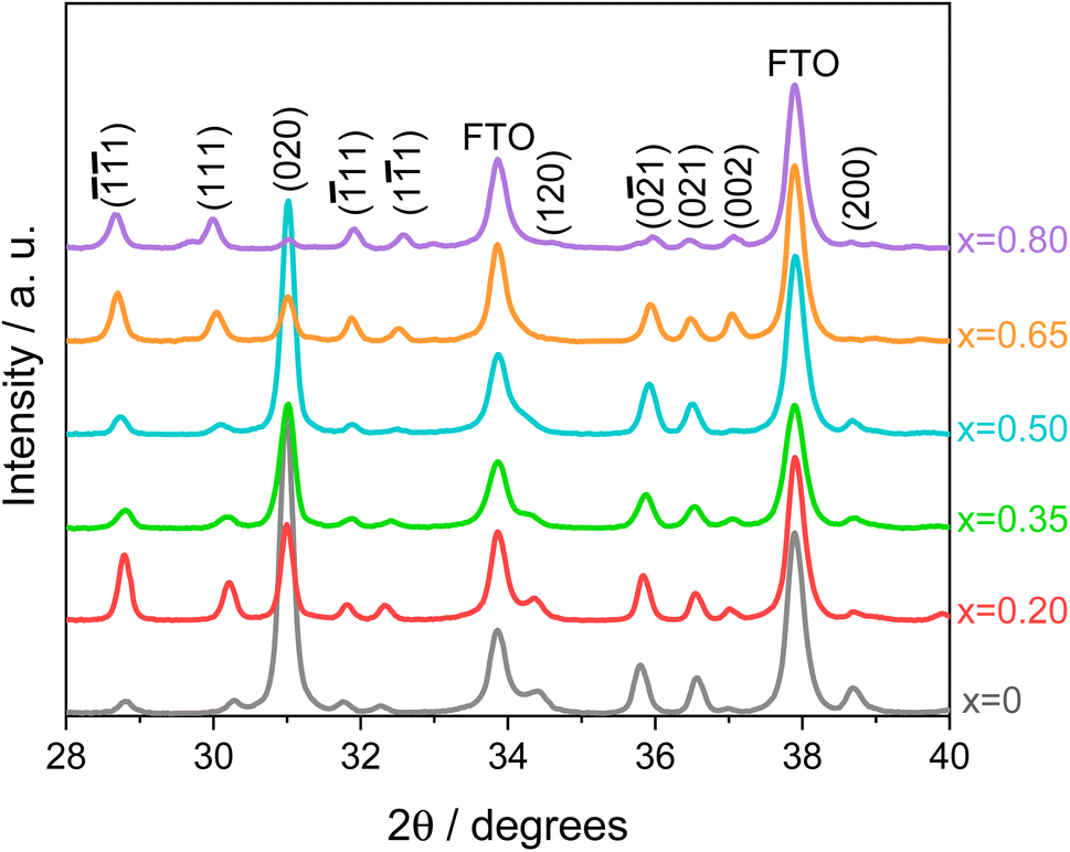 | ||
| Fig. 1 XRD patterns in the 28° to 40° 2θ region of CuW1−xMoxO4 electrodes, with x = 0–0.8. The characteristic Miller indices of pure CuWO4 wolframite single crystal structure (JCPDF 72-0616)34 are indicated. FTO peaks are also reported. | ||
Compared to the XRD pattern of pure CuWO4 (x = 0), a shift of the reflexes at 30.25° and 32.25° toward lower and higher 2θ values, respectively, is observed with progressively increasing Mo for W substitution (a detailed view of Fig. 1 is shown in Fig. S1 of the ESI file†), indicating the successful incorporation of Mo into the CuWO4 lattice.24,26 The characteristic wolframite peaks, well evident up to a 50% Mo for W substitution (x = 0.5), become progressively less marked for higher molybdenum contents (x = 0.65 and 0.80), probably due to the loss of wolframite structure in favour of the triclinic structure typical of α-CuMoO4 at room temperature,35 or to possible CuW1−xMoxO4 partial segregation into WO3 and CuMoO4.23
The LSV scans in water photo-oxidation conditions for all investigated electrodes with different Mo for W substitution are reported in Fig. 2A. By dividing the J values at 1.23 VRHE extracted from this figure by the maximum theoretical photocurrent density Jabs of each photoelectrode, calculated by integrating the absorption spectrum of each photoanode (Fig. S2†) over the solar spectrum, we obtained the photocurrent efficiency values J′ of each photoelectrode. To have a clearer insight of the effects of Mo for W substitution, we finally calculated the  values, reported in Fig. 2B, obtained as the ratio between the J′ value of each photoelectrode and the J′ value of pure CuWO4. The best performing electrode, in terms of both absolute photocurrent density under steady state condition and photocurrent onset at relatively low potentials, corresponds to the CuW0.5Mo0.5O4 film, obtained by 50% Mo for W substitution. In fact, Fig. 2B evidences a bell-shaped trend for the
  values for different Mo6+ for W6+ substitution (x = 0–0.8), with a maximum for 50% substitution, and a progressive photocurrent efficiency lowering for higher substitution degrees, with CuW0.2Mo0.8O4 performing even worse than pure CuWO4. Furthermore, a progressive shift of the photocurrent onset toward more positive potential values occurs with increasing Mo6+ ions incorporation (Fig. 2A). The origin of this optimum compromise is in line with the best charge separation efficiency attained upon optimum 50% Mo for W incorporation (Fig. S3†).
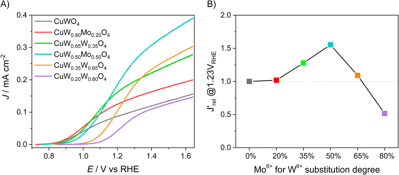 | ||
Fig. 2 (A) Linear sweep voltammetry (LSV) scans of CuW1−xMoxO4 films with different Mo6+ for W6+ substitution degrees, under back-side irradiation. (B) Trend of the relative photocurrent efficiency  , defined in the main text, vs. the percent of Mo for W substitution degree. , defined in the main text, vs. the percent of Mo for W substitution degree. | ||
Once assessed the optimal 50% Mo for W substitution, we investigated the effects of the photoactive layer thickness. The SEM top view and cross-section images of the optimum CuW0.5Mo0.5O4 material as 1-layered (1L), 2-layered (2L) and 3-layered (3L) films are shown in Fig. 3. Top views (Fig. 3A–C) account for a granular, grape-like shaped morphology for the 1L electrode that changes into a more compact and planar structure with increasing number of layers. This can be ascribed to the different particles packing degree consequent to the different number of annealing cycles required for the synthesis of multilayer electrodes (Table 1).
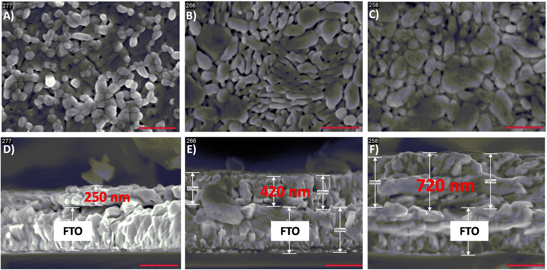 | ||
| Fig. 3 (A–C) Top view and (D–F) cross section SEM images at 50k× magnification of (A and D) CuW0.5Mo0.5O4 1L, (B and E) CuW0.5Mo0.5O4 2L and (C and F) CuW0.5Mo0.5O4 3L films. The scale bar is 500 nm. | ||
| Sample | Thickness/nm |
|---|---|
| 1L | 250 ± 30 |
| 2L | 420 ± 40 |
| 3L | 720 ± 60 |
From the calculation of the absorption coefficient (α) of the material at 420 nm, α = 7 × 10³ nm−1, and the relative absorption depth (δ, see Table S1†), the thinnest, ca. 250 nm thick, 1L film was found to be already able to absorb ca. 90% of the 420 nm incident radiation. Moreover, both LSV and IPCE analyses on CuW0.5Mo0.5O4 electrodes within the 250–720 nm thickness range (see Fig. S5†) account for the 250 nm thick photoactive layer (1L film) as the best performing one thanks to an optimum compromise between light absorption and charge separation efficiency.
Interestingly, the ca. 250 nm thick monolayer CuWMo electrode, obtained with 50% Mo for W substitution in the present study performs much better than the similarly thick CuW0.5Mo0.5O4 electrode prepared through a multilayer procedure,24 in terms of both higher J–V curve fill factor over the whole investigated potential range and photocurrent density at the 1.23 VRHE reference potential. Indeed, the lower number of depositions (each followed by annealing) ensures a lower number of interfaces, which may act as recombination centres. Furthermore, a better optical transparency allows for a more efficient use of the absorbed light.
3.2. PEC performance of CuW0.5Mo0.5O4 (CuWMo) vs. CuWO4 (CuW) photoelectrodes
The effective Mo for W substitution in CuW0.5Mo0.5O4 was proven by the energy-dispersive X-ray spectroscopy (EDX) mapping analyses reported in Table 2, accounting for a ca. equal co-presence of W and Mo in CuWMo.| Atom% | ||
|---|---|---|
| CuW | CuWMo | |
| Cu | 50.72 | 50.31 |
| W | 49.28 | 24.40 |
| Mo | — | 25.39 |
The SEM top view images of the CuW and CuWMo electrodes evidence a grape-like shaped morphology for both films (Fig. S6A and B†), with the molybdenum-containing material exhibiting a less compact structure, possibly facilitating the electrolyte/film contact across the whole film thickness. The cross-section images reported for the CuW (Fig. S6C†) and CuWMo (Fig. S6D†) electrodes account for a comparably thick photoactive layer of CuWO4 and CuW0.5Mo0.5O4 electrodes. The absorption spectra of CuW and CuWMo (Fig. S6E†) confirm a comparable thickness for these two electrodes, without any significant light scattering or absorption onset variation upon 50% Mo6+ for W6+ substitution.
The LSV and the IQE curves obtained with CuWMo in both back- and front-irradiation configurations are shown in Fig. 4 in comparison with those obtained with the CuW electrode. Upon 50% Mo for W substitution in CuWO4, a 6-fold enhancement in photocurrent production at 1.6 VRHE is attained (Fig. 4A) and a far higher photoactivity, extending to the visible region up to above 550 nm, as evidenced by the IQE plots in Fig. 4B. This confirms a far extended visible light exploitation. Moreover, the higher performance in front- with respect to back-side irradiation accounts for hole transport across the material bulk as more limiting than electron transport.
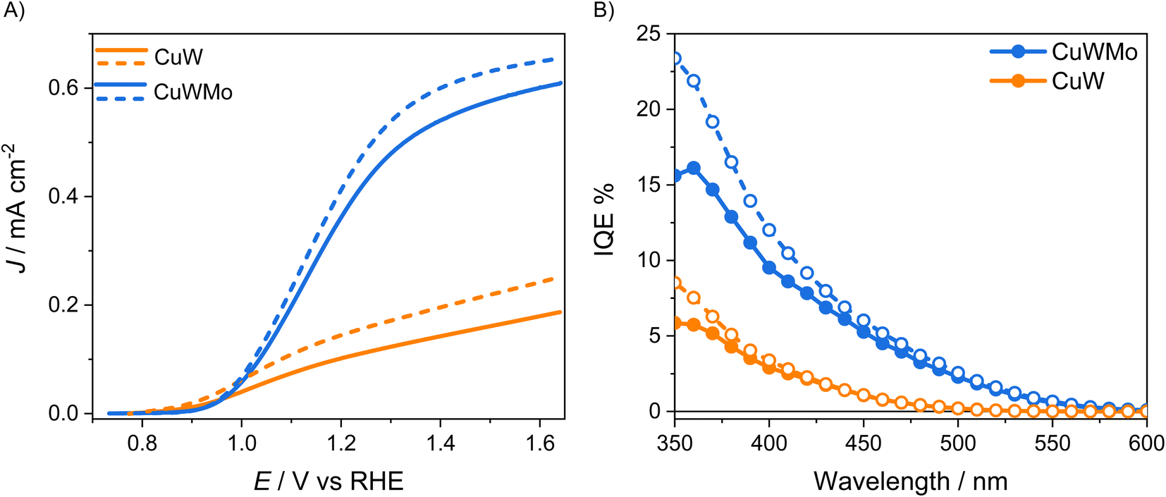 | ||
| Fig. 4 (A) Linear sweep voltammetry (LSV) and (B) internal quantum efficiency (IQE) curves at 1.23 VRHE of the CuWMo (blue) and CuW (orange lines) electrodes with comparable film thickness, in 0.1 M K3BO3, under back- (solid lines, full circles) and front-side irradiation (dashed lines, void circles). | ||
The charge injection and charge separation efficiency, ηinj and ηsep, respectively, of the CuW and CuWMo electrodes, calculated from LSV plots in the presence and absence of the NaNO2 hole scavenger as detailed in the ESI file,† are reported in Fig. 5, as a function of the applied potential. The ηinj and ηsep values of CuWMo at 1.23 VRHE are 52% and 6%, respectively, which point to charge separation in the material bulk as the main limiting factor for this material. Even lower is ηsep for CuW under the same conditions, which once again confirms the extremely low charge separation efficiency as main limitation of the PEC performance of copper tungstate.
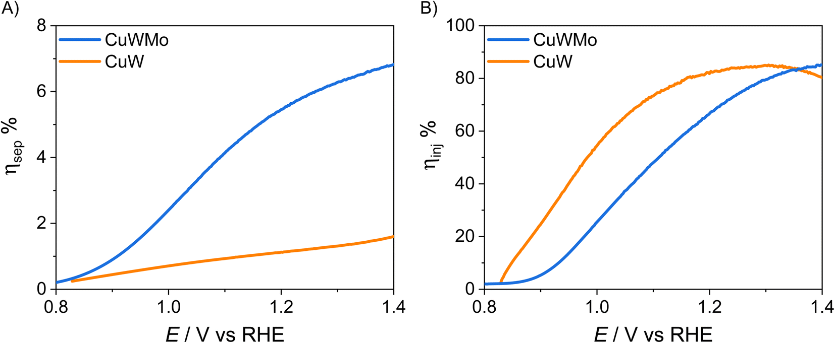 | ||
| Fig. 5 (A) Charge injection, ηinj, and (B) charge separation efficiency, ηsep, of CuWMo (blue) and CuW (orange) films vs. applied potential, under back-side irradiation. | ||
As shown in Fig. 5A, Mo for W substitution is beneficial over the whole investigated potential range, resulting in an almost 6-fold higher bulk charge separation at 1.23 VRHE, with a parallel modest decrease in surface charge injection efficiency (Fig. 5B). This is in line with the relative shift in photocurrent onset towards more positive potential values observed in LSV plots and tentatively attributed to additional trap surface states introduced in CuWO4 by Mo for W substitution.15–17,33,36
However, the ηsep and ηinj values estimated from measurements in the presence of sacrificial reagents may not be representative for water oxidation, especially under sluggish oxidation conditions, i.e., in the presence of a significant charge accumulation at the semiconductor–liquid junction. In fact, sacrificial redox agents involved in the electrochemical reaction at the film/electrolyte interface can affect band bending and charge accumulation, depending on their nature.37
On the other hand, intensity modulated photocurrent spectroscopy (IMPS) is a powerful tool in the frequency domain, which allows to unequivocally decouple the bulk and surface contributions of photoanodes by their respective time constants in operando, i.e., with the electrodes in contact with a buffered solution without any sacrificial species.38,39 Thus, a more accurate evaluation of ηsep and ηinj for the CuW and CuWMo electrodes was obtained through IMPS measurements in 0.1 M K3BO3 electrolyte solution. The IMPS response for the CuWMo and CuW films are shown in Fig. 6A as Nyquist plots of the complex photocurrent, at 1.6 VRHE.
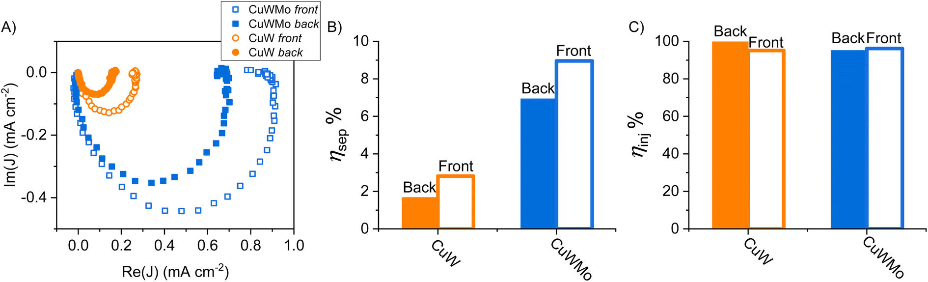 | ||
| Fig. 6 (A) IMPS analyses at 1.6 VRHE for CuWMo (blue) and CuW (orange) electrodes in 0.1 M K3BO3 under back- (full symbols) and front-side (void symbols) irradiation. The represented raw data were obtained upon normalization to the electron current recorded using the IMPS setup. (B) Charge separation (ηsep) and (C) charge injection (ηinj) efficiencies calculated from IMPS data under back- (filled columns) and front-side (void columns) irradiation. | ||
All Nyquist plots are typically composed of two semicircles, i.e., the negative semicircle located in the lower quadrant and representative of charge transport in the bulk (higher frequency process) and the positive semicircle located in the upper quadrant and associated with surface recombination (lower frequencies process).40 Notably, in all cases the surface recombination semicircle is significantly smaller than the bulk transport, indicating that a large steady state photocurrent is available for water oxidation at the photoanodes surface, as with other n-type metal oxides.41–43
The ηsep and ηinj values calculated in operando (see Section S3 in the ESI†) for each investigated electrode, under front- or back-side irradiation at 1.6 VRHE are reported as histograms in Fig. 6B and C. The far better bulk charge transport properties of the optimized CuWMo photoanode compared to the pure CuW electrode are confirmed by the more than 4-fold higher ηsep in both irradiation configurations (Fig. 6B), with no significant change in the ηinj of the original material (Fig. 6C). Noteworthy, far higher bulk electron transport compared to bulk hole transport is evidenced by the larger ηsep value obtained in front-rather than back-side irradiation, in line with the PEC performances presented in Fig. 4. IMPS results are in full agreement with those obtained in the presence of the NaNO2 hole scavenger (Fig. 5) and unequivocally demonstrate that the superior charge separation is the main origin of the far higher PEC performance of CuMoW with respect to CuW. This unequivocally attained ηsep increase is most likely related to the increased majority carrier concentration in 0.5% Mo-substituted CuWO4 with respect to pure CuWO4, with a consequent improved material conductivity also evidenced by Mott–Schottky analyses reported in previous studies for similar systems.23,25,26
3.3. The CuW0.5Mo0.5O4/BiVO4 heterojunction system
Aiming at exploiting possible synergies between CuW0.5Mo0.5O4, absorbing up to 550 nm, and BiVO4, having a 2.4 eV bandgap,9 an excellent conversion efficiency up to ca. 520 nm and a pronounced absorption shoulder in the 400–480 nm visible region (see absorption spectra in Fig. S6E†), we deposited a BiVO4 layer on top of the CuWMo electrode. The presence of the characteristic signals of monoclinic BiVO4 in the XRD pattern of the so obtained composite electrode (Fig. S7†), together with the same set of XRD peaks observed with CuWMo monolayer films, confirm the successful formation of the CuWMo/BV heterojunction. The presence of the BiVO4 overlayer on top of the CuWMo film induces a substantial absorption increase in the visible range up to 480 nm, particularly around 420 nm, where the absorption feature typical of BiVO4 is centred (Fig. S6E†). The top view morphology of the films significantly changes upon BiVO4 deposition (Fig. S8A†), switching from the granular grape-like shape observed for CuWMo (Fig. S6B†) to a more compact and planar structure, consequent to the deposition of successive BiVO4 layers and subsequent thermal cycles. The cross-section image relative to the CuWMo/BV heterojunction electrode (Fig. S8B†) does not allow an evaluation of the effective BiVO4 thickness due to the possible intercalation of the precursor solution throughout the porosity of the CuWMo underlayer, evidenced by the surface morphology change. From the increased absorption of the heterojunction at 420 nm upon BiVO4 deposition and the extinction coefficient of this latter,9 the BV overlayer was estimated to be ca. 170 nm thick.The LSV and IQE plots recorded with the CuWMo, CuWMo/BV and single BV electrodes under back- and front-side irradiation can be compared in Fig. 7 and 8, respectively.
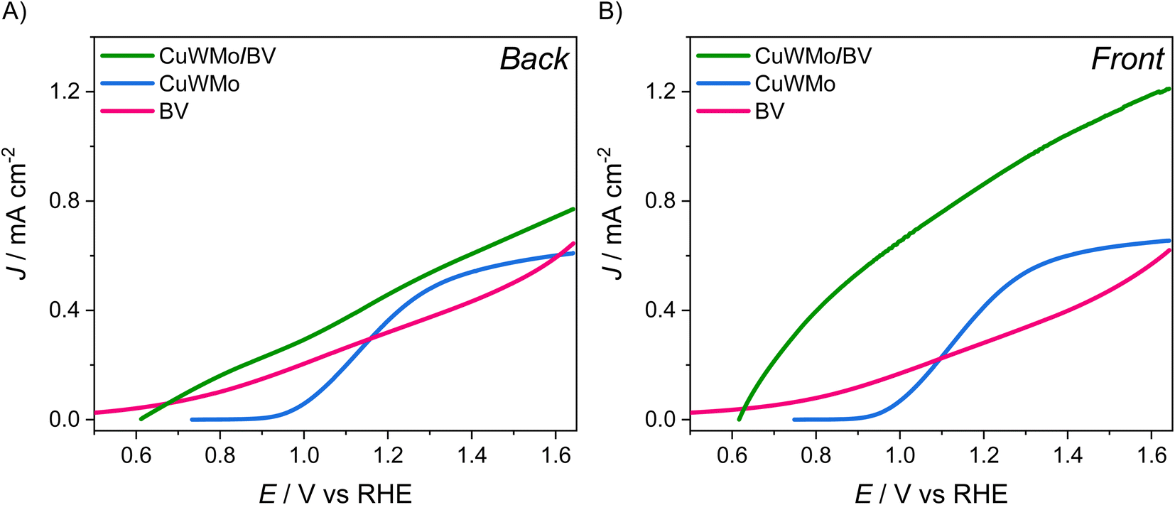 | ||
| Fig. 7 Linear sweep voltammetry (LSV) scans recorded with CuWMo (blue), BV (magenta) and CuWMo/BV electrode (green) under (A) back-side and (B) front-side irradiation. | ||
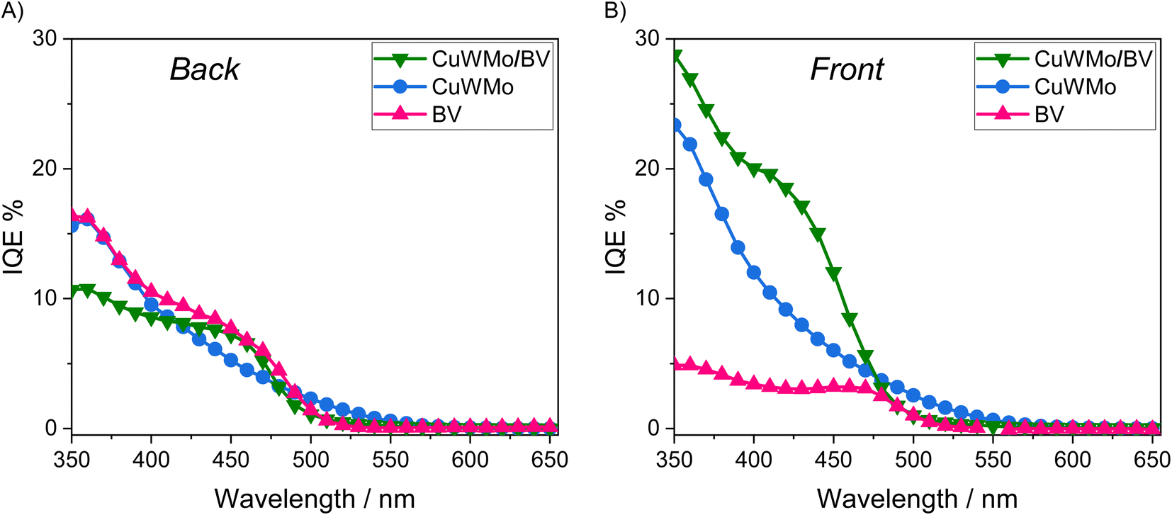 | ||
| Fig. 8 IQE plots recorded at 1.23 VRHE with the CuWMo (blue), BV (magenta) and CuWMo/BV (green) electrodes under (A) back-side and (B) front-side irradiation. | ||
As shown in Fig. 7A, under back-side irradiation the heterojunction system exhibits a slight LSV performance improvement in comparison to single CuWMo and BV, while under front-side irradiation the photoactivity enhancement is much larger (Fig. 7B). Moreover, BV deposition induces an appreciable earlier photocurrent onset in the J–V curves at lower applied potentials compared to that of the CuWMo single material, in line with the far energetically higher BiVO4 CB44 with respect to that of CuWO4-based materials.15,45,46
The IQE results at 1.23 VRHE (Fig. 8) evidence that any visible light photoactivity gain achieved upon coupling CuWMo with BV strongly depends on the irradiation configuration, which in turn implies the wavelength-dependent selective photoexcitation of one oxide, or rather the simultaneous excitation of the two coupled oxides in the heterojunction.47,48 Indeed, higher conversion efficiencies were selectively obtained with the heterojunction under front-rather than back-side irradiation (Fig. 8Avs.8B) and a strong dependence on the excitation wavelength is also outlined.
The peculiar behavior attained with the heterojunction system compared to the corresponding single oxide under the two irradiation configurations can be best envisaged in terms of the IQE enhancement factor reported in Fig. 9, and calculated according to the following equation:49
| IQEenhancement = IQECuWMo/BV − (IQECuWMo + IQEBV) | (4) |
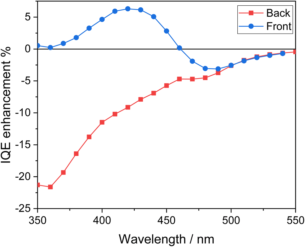 | ||
| Fig. 9 IQE enhancement factor calculated from the IQE data for the CuWMo/BV coupled electrode with respect to both single CuWMo and BV components. | ||
Under back-side irradiation the IQE enhancement factor is negative over the entire wavelength region. This indicates the lack of any synergism upon coupling the two oxides when CuWMo is excited first, so that a large portion of electron–hole couples, accounting for at least a 90% absorption of the radiation, are generated within CuWMo. The overall photoactivity decrease exhibited by the composite material, especially at λ < 400 nm where the incident light firstly excites the inner CuWMo layer, or at λ > 480 nm with photons selectively absorbed by the CuWMo compart, can be related to inefficient hole transfer from CuMoW through the BV overlayer. In the 400 < λ < 480 nm range, i.e., upon simultaneous excitation of both oxides, a charge recombination pathway at the interface of the two oxides may also occur, as already evidenced for WO3/BiVO4 heterojunctions.47,49,50
On the other hand, the IQE enhancement factor exhibits a different trend under front-side irradiation (Fig. 9). In particular, the negative IQE enhancement factor in the wavelength region where BV does not strongly absorb (λ > 480 nm) evidences that the selective excitation of the inner CuWMo layer in the composite is not followed by any effective hole transfer toward the electrolyte through the BV overlayer (Fig. 10A). This confirms the inability of CuWMo to sensitise BV in the longer wavelength region, as also observed under back-side irradiation (Fig. 9).
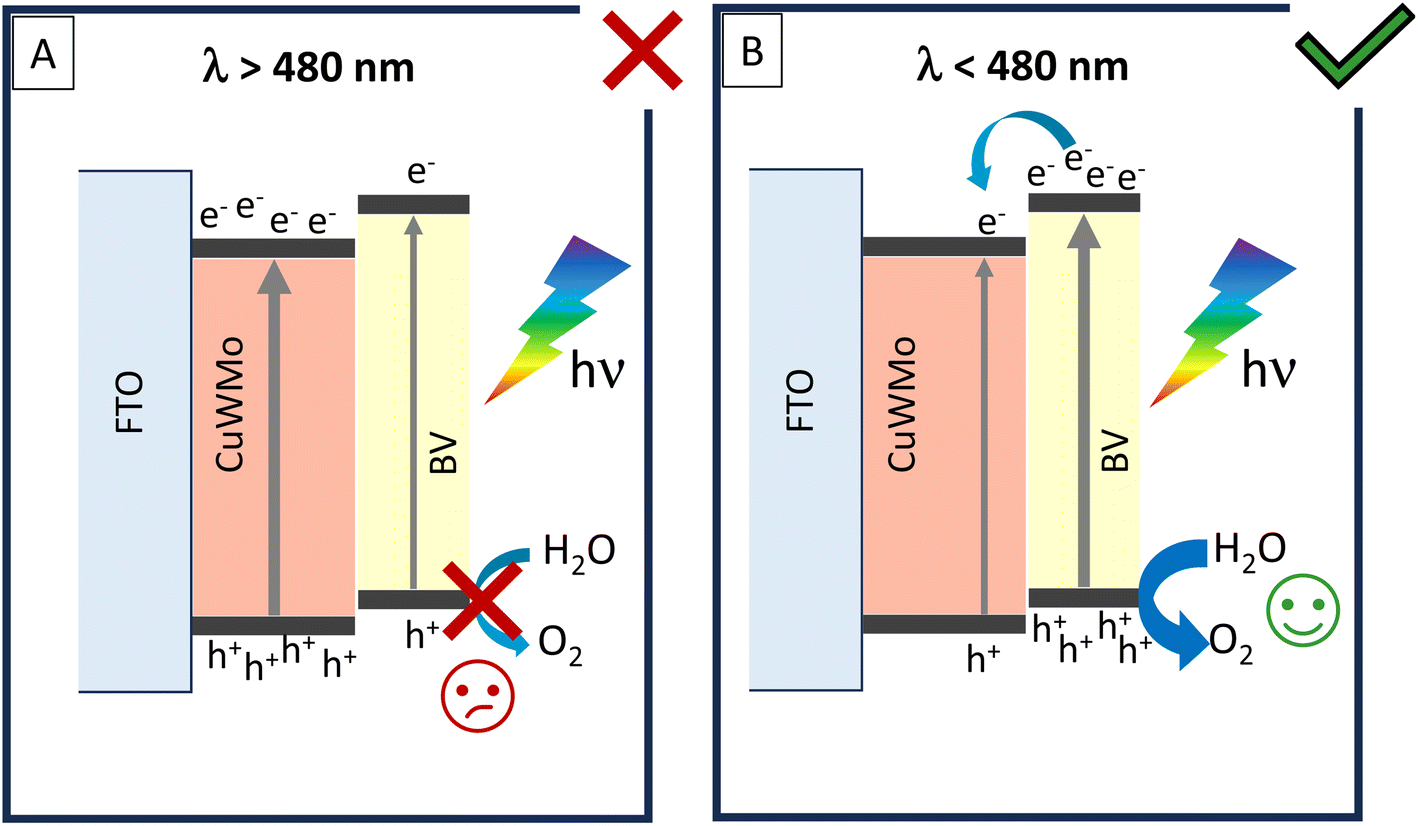 | ||
| Fig. 10 Photoactivation processes in the CuWMo/BV heterojunction under front-side irradiation at wavelengths (A) above 480 nm and (B) below 480 nm. | ||
On the other hand, at λ < 480 nm, where BV is the main absorbing layer, the IQE enhancement factor under front-side irradiation tends to become positive (Fig. 9), and it is no more superimposed to that observed under back-side irradiation. The charge carriers photogenerated in BV may fully exploit the staggered band edge alignment at the interface between the two oxides, with a consequent more efficient charge separation across the composite system (Fig. 10B), determining a maximum IQE enhancement factor value at ca. 420 nm, where BV exhibits its highest absorption and photoactivity. This positive synergism, guaranteed by the correct type II band alignment established at the interface of the two coupled oxides, results in the most significant gain in performance achieved upon semiconductors coupling in this configuration.
4. Conclusions
A 250 nm-thick CuW0.5Mo0.5O4 photoanode material with 50% Mo for W substitution, prepared through an effective one step deposition method, has been identified as optimal PEC performing in terms of both dopant content and film thickness.Intensity modulated photocurrent spectroscopy (IMPS) analysis demonstrated that the superior PEC performance of CuW0.5Mo0.5O4 results from a more efficient separation of photoproduced charges with respect to CuWO4.
Coupling the CuW0.5Mo0.5O4 photoanode with BiVO4 in a heterojunction allowed for a synergistic charge separation improvement in the 350–480 nm visible range under front-side irradiation, where BiVO4 behaves as main light photoabsorbing layer and has maximum photoactivity. This does not occur under back-side irradiation, when CuWMo first gets excited, because the coupled system is unable to efficiently transfer holes through the unexcited BiVO4 layer.
This work demonstrates that the combination of different modification strategies can be effectively exploited to enhance the relatively low PEC performance of the extremely stable, but poorly investigated, CuWO4 system.
Data availability
All data generated or analyzed during this study are included in this published article and its ESI files.†Conflicts of interest
There are no conflicts to declare.Acknowledgements
The collaboration of Dr Marco Bompieri in performing photo(electro)catalytic experiments is gratefully acknowledged. This work was supported by the Cariplo Foundation 2021-0664 Project entitled “Carbon dioxide conversion into energy-rich molecules with tailored catalysts” (CO2EnRich) and received partial financial support from MUR (Italy), through the PRIN MAPEC (No. 2022599NR3) and PRIN CHARM (No. 20227TKTMY) projects.References
- N. S. Lewis and D. G. Nocera, Proc. Natl. Acad. Sci. U. S. A., 2006, 103, 15729–15735 CrossRef CAS.
- N. S. Lewis, Science, 2016, 351, 6271 CrossRef.
- M. Grätzel, Nature, 2001, 414, 338–344 CrossRef.
- A. Fujishima and K. Honda, Nature, 1972, 238, 37–38 CrossRef CAS.
- K. Sivula and R. van de Krol, Nat. Rev. Mater., 2016, 1, 15010 CrossRef CAS.
- D. K. Lee, D. Lee, M. A. Lumley and K.-S. Choi, Chem. Soc. Rev., 2019, 48, 2126–2157 RSC.
- Y. Tang, N. Rong, F. Liu, M. Chu, H. Dong, Y. Zhang and P. Xiao, Appl. Surf. Sci., 2016, 361, 133–140 CrossRef CAS.
- L. A. Cipriano, G. Di Liberto, S. Tosoni and G. Pacchioni, J. Chem. Theory Comput., 2020, 16, 3786–3798 CrossRef CAS.
- A. Polo, M. V. Dozzi, I. Grigioni, C. Lhermitte, N. Plainpan, L. Moretti, G. Cerullo, K. Sivula and E. Selli, Sol. RRL, 2022, 6, 2200349 CrossRef CAS.
- M. Tayebi and B. K. Lee, Renewable Sustainable Energy Rev., 2019, 111, 332–343 CrossRef CAS.
- J. H. Kim, J.-W. Jang, Y. H. Jo, F. F. Abdi, Y. H. Lee, R. van de Krol and J. S. Lee, Nat. Commun., 2016, 7, 13380 CrossRef CAS.
- S. Wang, P. Chen, Y. Bai, J.-H. Yun, G. Liu and L. Wang, Adv. Mater., 2018, 30, 1800486 CrossRef.
- L. Chen, W. Li, W. Qiu, G. He, K. Wang, Y. Liu, Q. Wu and J. Li, ACS Appl. Mater. Interfaces, 2022, 14, 47737–47746 CrossRef CAS.
- S. Farhoosh, B. Eftekharinia, M. Tayebi, B. K. Lee and N. Naseri, Appl. Surf. Sci., 2021, 550, 149374 CrossRef CAS.
- C. R. Lhermitte and B. M. Bartlett, Acc. Chem. Res., 2016, 49, 1121–1129 CrossRef CAS.
- J. E. Yourey, K. J. Pyper, J. B. Kurtz and B. M. Bartlett, J. Phys. Chem. C, 2013, 117, 8708–8718 CrossRef CAS.
- Y. Gao and T. W. Hamann, J. Phys. Chem. Lett., 2017, 8, 2700–2704 CrossRef CAS.
- W. Ye, F. Chen, F. Zhao, N. Han and Y. Li, ACS Appl. Mater. Interfaces, 2016, 8, 9211–9217 CrossRef CAS.
- I. Grigioni, A. Polo, C. Nomellini, L. Vigni, A. Poma, M. V. Dozzi and E. Selli, ACS Appl. Energy Mater., 2023, 6, 10020–10029 CrossRef CAS.
- C. M. Tian, M. Jiang, D. Tang, L. Qiao, H. Y. Xiao, F. E. Oropeza, J. P. Hofmann, E. J. M. Hensen, A. Tadich, W. Li, D. C. Qi and K. H. L. Zhang, J. Mater. Chem. A, 2019, 7, 11895–11907 RSC.
- C. Nomellini, A. Polo, I. Grigioni, G. Marra, M. V. Dozzi and E. Selli, Photochem. Photobiol. Sci., 2023, 22, 2759–2768 CrossRef CAS.
- D. Bohra and W. A. Smith, Phys. Chem. Chem. Phys., 2015, 17, 9857–9866 RSC.
- J. C. Hill, Y. Ping, G. A. Galli and K.-S. Choi, Energy Environ. Sci., 2013, 6, 2440–2446 RSC.
- A. Polo, C. Nomellini, I. Grigioni, M. V. Dozzi and E. Selli, ACS Appl. Energy Mater., 2020, 3, 6956–6964 CrossRef CAS.
- J. Yang, C. Li and P. Diao, Electrochim. Acta, 2019, 308, 195–205 CrossRef CAS.
- Q. Liang, Y. Guo, N. Zhang, Q. Qian, Y. Hu, J. Hu, Z. Li and Z. Zou, Sci. China Mater., 2018, 61, 1297–1304 CrossRef CAS.
- D. Wang, P. Bassi, H. Qi, X. Zhao, Gurudayal, L. Wong, R. Xu, T. Sritharan and Z. Chen, Materials, 2016, 9, 348 CrossRef.
- S. K. Pilli, T. G. Deutsch, T. E. Furtak, L. D. Brown, J. A. Turner and A. M. Herring, Phys. Chem. Chem. Phys., 2013, 15, 3273–3278 RSC.
- I. Rodríguez-Gutiérrez, E. Djatoubai, M. Rodríguez-Pérez, J. Su, G. Rodríguez-Gattorno, L. Vayssieres and G. Oskam, Electrochim. Acta, 2019, 308, 317–327 CrossRef.
- F. Zhan, J. Li, W. Li, Y. Liu, R. Xie, Y. Yang, Y. Li and Q. Chen, Int. J. Hydrogen Energy, 2015, 40, 6512–6520 CrossRef CAS.
- S. Selim, L. Francàs, M. García-Tecedor, S. Corby, C. Blackman, S. Gimenez, J. R. Durrant and A. Kafizas, Chem. Sci., 2019, 10, 2643–2652 RSC.
- A. Polo, I. Grigioni, M. V. Dozzi and E. Selli, Catal. Today, 2020, 340, 19–25 CrossRef CAS.
- K. J. Pyper, J. E. Yourey and B. M. Bartlett, J. Phys. Chem. C, 2013, 117, 24726–24732 CrossRef CAS.
- J. E. Yourey and B. M. Bartlett, J. Mater. Chem., 2011, 21, 7651–7660 RSC.
- S. C. Abrahams, J. L. Bernstein and P. B. Jamieson, J. Chem. Phys., 1968, 48, 2619–2629 CrossRef CAS.
- Y. Gao and T. W. Hamann, Chem. Commun., 2017, 53, 1285–1288 RSC.
- D. Klotz, D. A. Grave and A. Rothschild, Phys. Chem. Chem. Phys., 2017, 19, 20383–20392 RSC.
- E. A. Ponomarev and L. M. Peter, J. Electroanal. Chem., 1995, 396, 219–226 CrossRef.
- D. Klotz, D. S. Ellis, H. Dotan and A. Rothschild, Phys. Chem. Chem. Phys., 2016, 18, 23438–23457 RSC.
- F. Boudoire, Y. Liu, F. Le Formal, N. Guijarro, C. R. Lhermitte and K. Sivula, J. Phys. Chem. C, 2021, 125, 10883–10890 CrossRef CAS.
- Y. Liu, F. Le Formal, F. Boudoire, L. Yao, K. Sivula and N. Guijarro, J. Mater. Chem. A, 2019, 7, 1669–1677 RSC.
- Y. Liu, F. Le Formal, F. Boudoire and N. Guijarro, ACS Appl. Energy Mater., 2019, 2, 6825–6833 CrossRef CAS.
- A. Polo, F. Boudoire, C. R. Lhermitte, Y. Liu, N. Guijarro, M. V. Dozzi, E. Selli and K. Sivula, J. Mater. Chem. A, 2021, 9, 27736–27747 RSC.
- J. K. Cooper, S. Gul, F. M. Toma, L. Chen, P. A. Glans, J. Guo, J. W. Ager, J. Yano and I. D. Sharp, Chem. Mater., 2014, 26, 5365–5373 CrossRef CAS.
- I. Grigioni, A. Polo, M. V. Dozzi, L. Ganzer, B. Bozzini, G. Cerullo and E. Selli, J. Phys. Chem. C, 2021, 125, 5692–5699 CrossRef CAS.
- H. V. Thang, E. Albanese and G. Pacchioni, J. Phys.: Condens.Matter, 2019, 31, 145503 CrossRef.
- I. Grigioni, K. G. Stamplecoskie, D. H. Jara, M. V. Dozzi, A. Oriana, G. Cerullo, P. V. Kamat and E. Selli, ACS Energy Lett., 2017, 2, 1362–1367 CrossRef CAS.
- I. Grigioni, M. Abdellah, A. Corti, M. V. Dozzi, L. Hammarström and E. Selli, J. Am. Chem. Soc., 2018, 140, 14042–14045 CrossRef CAS.
- I. Grigioni, M. V. Dozzi and E. Selli, J. Phys.: Condens.Matter, 2020, 32, 014001 CrossRef CAS.
- I. Grigioni, A. Polo, M. V. Dozzi, K. G. Stamplecoskie, D. H. Jara, P. V. Kamat and E. Selli, ACS Appl. Energy Mater., 2022, 5, 13142–13148 CrossRef CAS.
Footnote |
| † Electronic supplementary information (ESI) available. See DOI: https://doi.org/10.1039/d4se00161c |
| This journal is © The Royal Society of Chemistry 2024 |