DOI:
10.1039/C6RA07103A
(Paper)
RSC Adv., 2016,
6, 56149-56158
Experimental investigations on NO2 sensing of pure ZnO and PANI–ZnO composite thin films
Received
17th March 2016
, Accepted 24th May 2016
First published on 26th May 2016
Abstract
In the present work, comparative investigations on NO2 gas sensing properties of the hybrid nanocomposite thin films of polyaniline (PANI), ZnO and PANI–ZnO towards NO2 gas at room temperature have been reported. The effect of concentration of PANI in the composite thin films on NO2 gas sensing has been investigated. Structural and surface morphological characterizations have been carried out using X-ray diffraction (XRD) and scanning electron microscopy (SEM) respectively. The presence of 5 wt% PANI in the composite films was found to give a maximum sensing response of ∼6.11 × 10² towards 20 ppm NO2 gas having fast response and recovery time of about 2.16 min and 3.5 min respectively.
1. Introduction
The emission of nitrogen dioxide (NO2) which has a bad effect on public health and the environment is motivating extensive scientific and technological research in the field of NO2 sensing. The detection of NO2 is quite necessary because of its characteristic pungent odor, toxicity and dangerousness, even at very low concentration. The use of conducting polymers as sensing elements in chemical sensors is a center of attraction due to their high sensitivity with the change of the electrical and optical properties when exposed to different types of gases or liquids.1 Polyaniline (PANI) is one of the most prominent materials among the variety of conducting polymers due to its unique electrical property, environmental stability, easy fabrication process and intrinsic redox reaction.1–4 PANI has also been used in different applications such as gas sensor5 rechargeable batteries6 and photovoltaic cells.7 However, the problems with these conducting polymers regarding the yield are their low processing ability, poor chemical stability and mechanical strength.8 The fabrication of hybrid composite of conducting polymers with metal oxides seems to be attractive to resolve these issues and concerns. However, no much effort has been made towards development of a hybrid composite of PANI and ZnO especially for detection of NO2 gas at room temperature.9 Alternatively, the metal oxides are advantageous in these aspects but demands high operating temperatures.10–12 Among the inorganic materials, nanocrystalline ZnO is one of the most attractive and extensively used materials for detection of the LPG, NH3, NO2 and UV.13–16 In the present work, nanoparticles of PANI and ZnO were synthesized and their hybrid composites were prepared for the detection of NO2 gas. In this context, humidity is a common cross-contaminant that can be varied widely in concentration with changes in ambient conditions due to NO2 gas. Therefore, variations of concentration of PANI in ZnO composite thin film with exposure of different concentration of NO2 gas have been investigated and found that sensor is highly responsive, having good selectivity and better reproducibility with functionality at room temperature.
2. Experimental
2.1 Fabrication of PANI–ZnO nanocomposite thin film sensor
PANI was prepared by polymerization of aniline. For this process hydrochloric acid was used which acts as dopant for PANI molecules and bound with the central N atom of aniline molecule like.17 Nanostructured ZnO was prepared using chemical route as prescribed in our earlier paper.18 The prepared PANI was added to ZnO nanoparticles (NPs) sol. in different concentrations (0 wt%, 1 wt%, 5 wt% and 10 wt%). The PANI incorporated ZnO nanoparticles suspension was sintered at 100 °C in air for 2 h for producing powder form. Thin films of pure PANI, ZnO NPs and ZnO–PANI composites were prepared on corning glass substrates by spin coating technique at 2200 rpm for 30 s and dried on hot plate at 100 °C for 10 min.19–22 The thickness of the pure PANI film, pure ZnO film and PANI–ZnO film were measured by using Dektak profile meter (Veeco Dektak 150 surface profiler) and was found to be 210 nm, 290 nm and 320 nm respectively. For the gas sensing application, films were deposited on inter digital electrode (IDEs) patterned corning glass substrates by spin coating of the respective solutions.
2.2 Gas sensing properties measurements
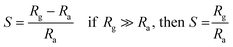
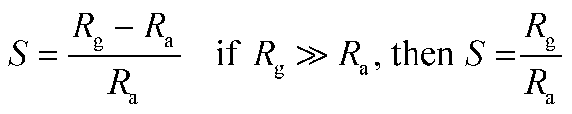
NO2 gas sensor was designed and fabricated which is based on the variations of electrical resistance with exposure of gas. Pt sputtered inter digital electrode was fabricated on a 1 × 1 cm2 corning glass substrate to form a transducer, which were used directly to measure the change in resistance of the sensitive PANI–ZnO composite thin film layer with exposure of NO2 gas of various concentrations. The device was placed inside a steel box having volume 11 L, then allow to a certain amount of NO2 gas to inject into the test chamber, the resistance was reached to a steady value in open air as shown in Fig. 1(a). A Keithley 2700 digital multi-meter interfaced with a computer data acquisition system was used to measure the variations in resistance of the sensor. The measurements were performed at room temperature. The sensor response towards an oxidizing gas such as NO2 is defined as:11| |
 | (1) |
where, Ra and Rg are the resistances of the sensor structure in the presence of atmospheric air and target gas respectively. The response time was measured as the time taken by the sensor to acquire the 90% of its maximum resistance value in the presence of target oxidizing gas. Once the maximum resistance value was attained, the target gas was flushed out from the test chamber and later the sensor was irradiated by a 200 W bulb which provides necessary thermal energy for removing the chemisorbed NO2 or moisture from the film surface. Lastly sensor was allowed to regain its initial resistance value in atmospheric air at the room temperature. The time taken by the sensor to reacquire about 10% higher value compared to its initial resistance in the presence of atmospheric air is considered as the recovery time.
 |
| | Fig. 1 (a) Schematic diagram of sensing device and (b) schematic illustrating the mechanism of formation of ZnO/PANI heterojunction microstructures. | |
2.3 Formation mechanism
ZnO is formed according to the following equation:| | |
Zn(CH3COO)2 + 2CH3CH2OH → (CH3CH2O−)2Zn2+ + 2CH3COOH
| (2) |
| | |
LiOH + CH3CH2OH ↔ CH3CH2O−Li+ + H2O
| (3) |
| | |
(CH3CH2O−)2Zn2+ + 2LiOH → Zn(OH)2 + 2CH3CH2OLi
| (4) |
The zinc acetate dihydrate was dissolved in the boiling ethanol at atmospheric pressure and subsequently allowed to cool at room temperature to give a transparent and stable Zn based precursor CH3CH2O−Zn+. When LiOH was added to precursor (CH3CH2O−)2Zn2+, Zn(OH)2 was obtained after the chemical reaction and CH3CH2OLi evaporated. Calcinations of corresponding reaction precursors yielded the ZnO nanocrystals. We have proposed a plausible mechanism for the formation of ZnO/PANI heterojunction microstructures, as schematically illustrated in Fig. 1(b).
2.4 Characterization
X-ray diffraction (XRD) studies were carried out using a X-ray diffractometer (Bruker D8 Discover). The XRD patterns were recorded in the 2θ range of 10–70° with step width 0.02° and step time 0.9 s using CuKα1 radiation (λ = 0.15418 nm). The morphology of the ZnO and ZnO/PANI films were examined using Scanning Electron Microscope (JEOL, JSM-6490LV). Chemical structure of thin film was examined by FTIR technique (model: Bruker Tensor 27) using undoped KBr as reference. UV-vis spectra of the samples, which were dispersed in de-ionized water in an ultrasonic bath, were recorded on the evaluation 201 UV-visible spectrophotometer.
3. Results and discussion
3.1 Structural studies
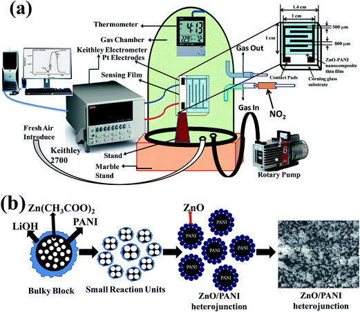
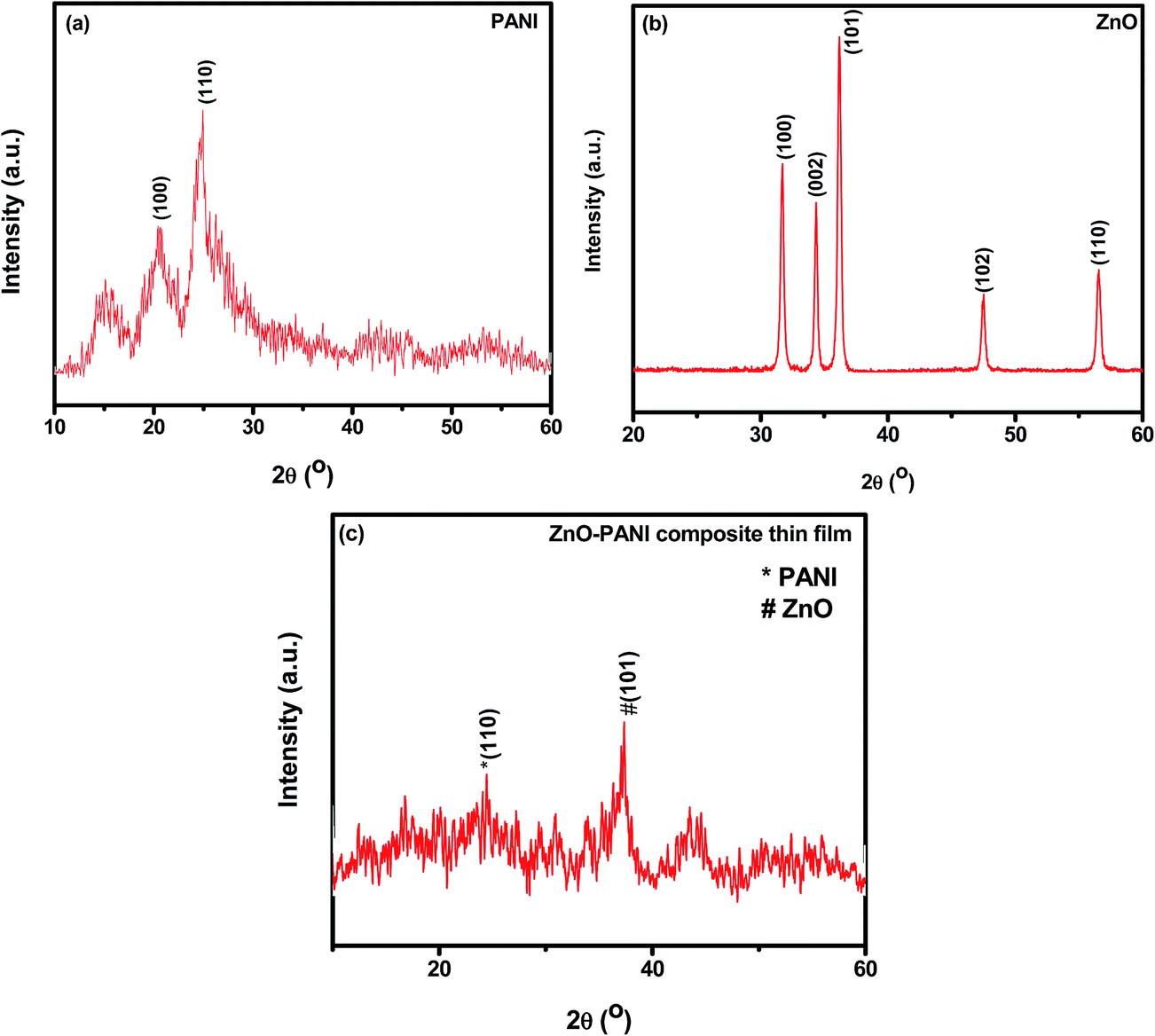
Fig. 2(a)–(c) represent the X-ray diffraction (XRD) patterns of the pure PANI, pure ZnO and ZnO–PANI composite thin films respectively. The XRD pattern of pure PANI (Fig. 2(a)) shows the reflection peaks occur at 2θ = 24.61° and 20.60° which corresponds to (110) and (100) plane of PANI respectively. An additional peak at 2θ ≈ 15.06° is also observed and is in agreement with the reported value.15 Fig. 2(b) shows the XRD pattern with the peaks corresponding to reflection planes (100), (002), (101), (102) and (110) of the wurtzite polycrystalline structure of ZnO.22 X-ray diffraction pattern of composite ZnO–PANI as shown in Fig. 2(c) revealed the amorphous character prominently with weak reflections corresponding to ZnO.22,23 It appears that the molecular chains of PANI are stretched leading to decrease in crystallinity of hybrid composite film. Average crystallite was calculated as 5.66 nm.
 |
| | Fig. 2 X-ray diffraction patterns of (a) pure PANI, (b) ZnO, and (c) ZnO–PANI. | |
3.2 Scanning electron microscope (SEM)
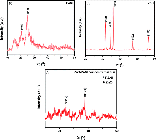
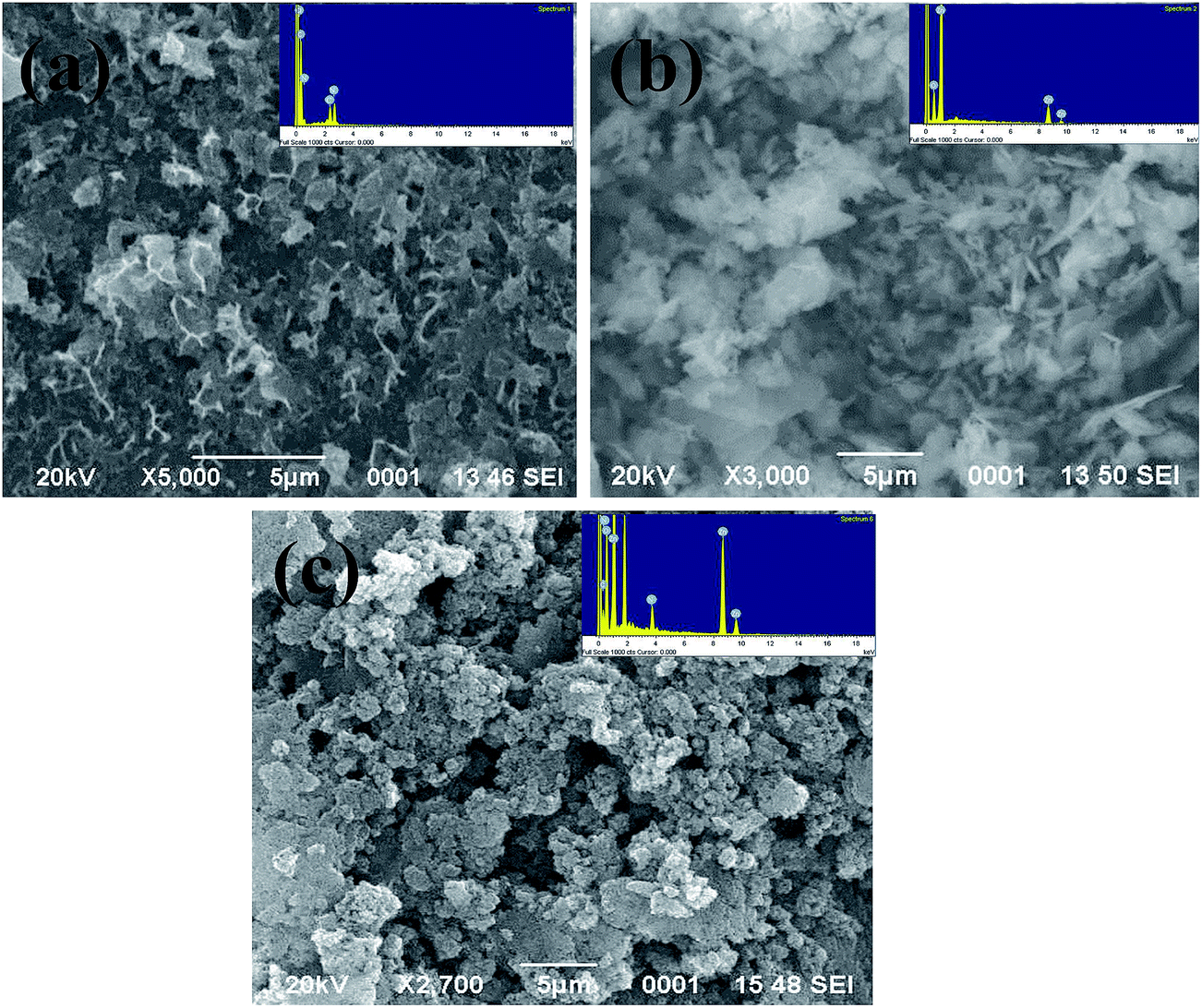
Fig. 3(a)–(c) show the SEM images of pure PANI, ZnO nanoparticles and ZnO–PANI composite thin films respectively. The elemental analysis of PANI, ZnO and ZnO–PANI has also been recorded by EDX and is shown as inset figures of Fig. 3. The SEM image of the pure PANI film (Fig. 3(a)) exhibits a fibrous structure with many pores. Fig. 3(b) shows the flower shaped surface morphology of the ZnO thin film annealed at 400 °C for 2 h. The SEM image of the composite thin film (Fig. 3(c)) shows the agglomeration free and uniform distribution of the PANI in ZnO thin film matrix. It can be seen that the PANI chains are closely surrounded with the mesh like structure built by ZnO nanoparticles. The obtained rough and porous morphology of prepared thin film as shown in Fig. 3(c) provided the high surface to volume ratio which enhanced the sensing response.
 |
| | Fig. 3 Scanning electron micrographs of (a) PANI, (b) ZnO and (c) PANI–ZnO composites thin film. | |
3.3 Optical properties
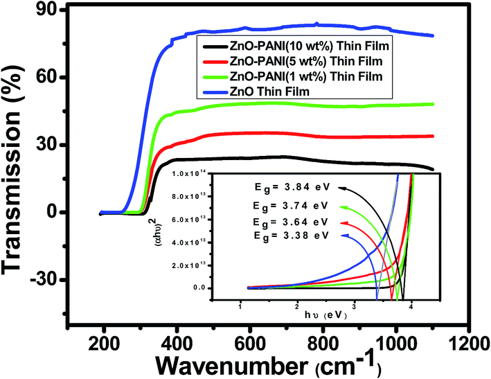
The optical transmission spectra of ZnO and ZnO–PANI with 1 wt%, 5 wt% and 10 wt% thin films having thickness 300 nm each deposited separately on corning glass substrate were measured in the wavelength range of 190 to 1100 nm, and the variation is shown in Fig. 4. ZnO and ZnO–PANI thin films exhibit a high transmission (90–20%) in the visible region and show a sharp fundamental absorption edge at ∼340 nm.
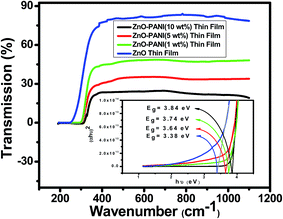 |
| | Fig. 4 Transmission spectra of ZnO, ZnO–PANI (3 wt%), ZnO–PANI (5 wt%) and ZnO–PANI (10 wt%) composite thin films and inset Tauc plot (αhν)2 vs. hν of ZnO, ZnO–PANI (3 wt%), ZnO–PANI (5 wt%) and ZnO–PANI (10 wt%) composite thin films. | |
Optical band gap of the ZnO and ZnO–PANI thin films deposited on corning glass substrate, were calculated from the intercept on energy axis obtained by extrapolating the linear portion of the Tauc plot of (αhν)2 vs. photon energy (hν) as shown inset Fig. 4. Estimated value of band gap for as-grown ZnO thin film is found to be 3.38 eV which is close to the actual values for ZnO thin films (3.3 eV) grown by various techniques.14,15 The variation in band gap shows the electronic interaction between ZnO and PANI confining the formation of ZnO–PANI composite thin film. It indicates that insertion of ZnO nanoparticles has the effect on the doping of conducting polyaniline, while this effect should owe to an interaction at the interface of polyaniline and ZnO nanoparticles. In the case of ZnO–PANI nanocomposite, the peak around 380 nm is ascribed to the selective interaction between ZnO and quinoid ring of polyaniline.
3.4 FTIR spectra
FTIR spectrum is the feature of a particular compound that gives the information about its functional groups, molecular geometry and molecular interactions. Fig. 5 shows the FTIR spectra of pure PANI, ZnO NPs and PANI/ZnO hybrid nanocomposites. Fig. 5(a) shows that the characteristic peaks of pure PANI appeared at 1631, 1471, 1292 and 1121 cm−1. FTIR spectrum of ZnO-NPs (Fig. 5(b)) exhibits the peak at 475 cm−1 which is due to the stretching mode of ZnO-NPs and addition peak at 1380 cm−1 is due to leading vibration of C–H in the methyl and 1640 cm−1 attributed to the leading vibration molecule.24 Fig. 5(c) shows that the absorption peaks for PANI/ZnO nanocomposites appear at 1572 cm−1 is due to C![[double bond, length as m-dash]](https://www.rsc.org/images/entities/char_e001.gif) C stretching mode of the quinoid rings, 1465 cm−1 is due to CC stretching mode of benzenoid rings, 1234 cm−1 is attributed to C–N stretching mode and 1148 cm−1 can be attributed to the in-plane and out-of plane C–H bending,25 indicating the formation of PANI in the composites. Comparing to the corresponding peaks of pure PANI, the peaks of PANI/ZnO shifted towards higher and lower wave numbers. This shifting of absorption bands may be due to the action of hydrogen bonding between the hydroxyl groups on the surface of ZnO nanoparticles and the amine groups in the PANI molecular chains.26
C stretching mode of the quinoid rings, 1465 cm−1 is due to CC stretching mode of benzenoid rings, 1234 cm−1 is attributed to C–N stretching mode and 1148 cm−1 can be attributed to the in-plane and out-of plane C–H bending,25 indicating the formation of PANI in the composites. Comparing to the corresponding peaks of pure PANI, the peaks of PANI/ZnO shifted towards higher and lower wave numbers. This shifting of absorption bands may be due to the action of hydrogen bonding between the hydroxyl groups on the surface of ZnO nanoparticles and the amine groups in the PANI molecular chains.26
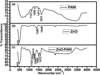 |
| | Fig. 5 FTIR spectra obtained for (a) PANI (b) ZnO-NPs (c) ZnO–PANI composite. | |
3.5 Sensing behaviour
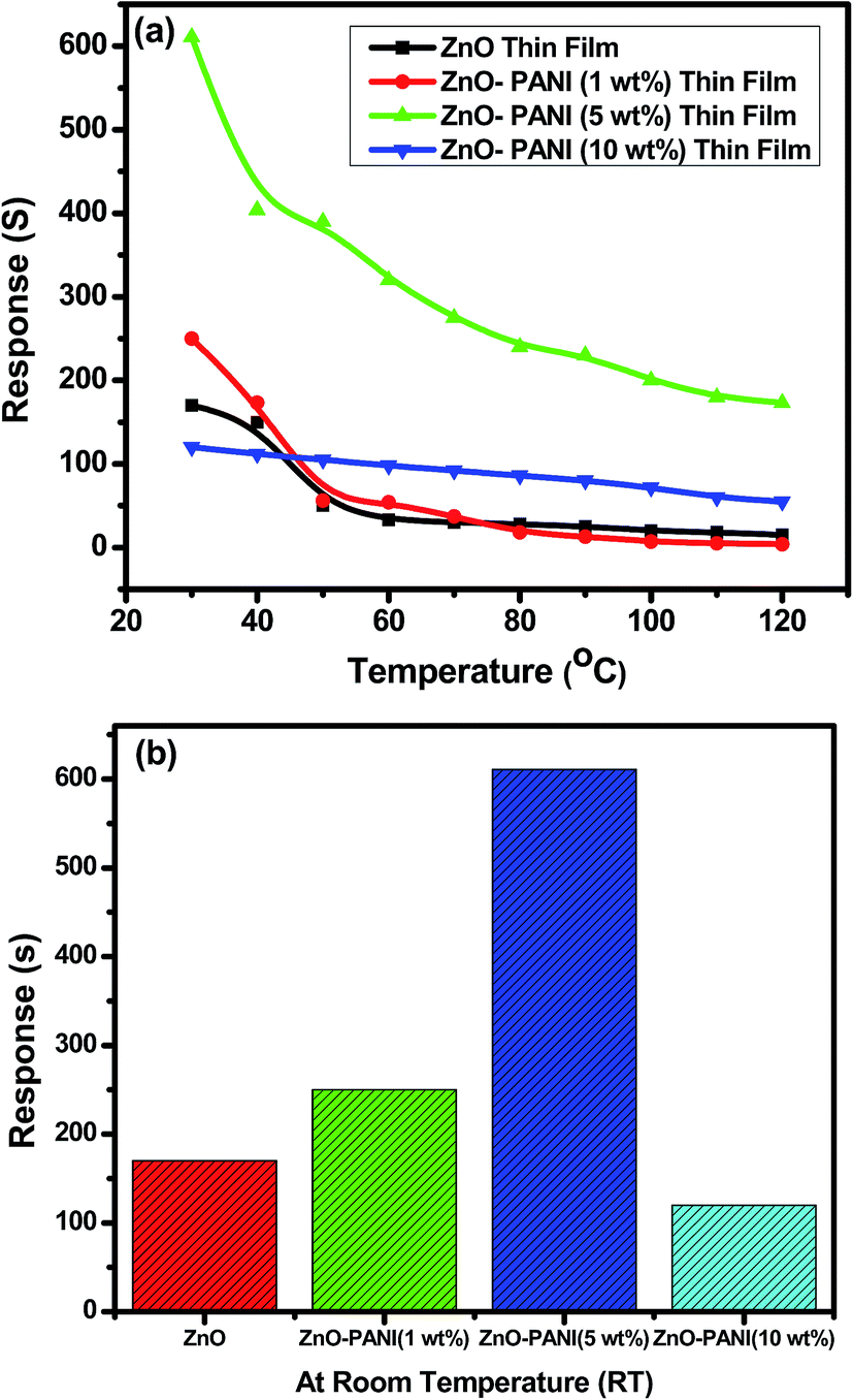
Fig. 6(a) shows the variation in sensing response of thin film sensors of Pure ZnO and ZnO with different concentrations of PANI as 1 wt%, 5 wt% and 10 wt% as a function of temperature towards 20 ppm of NO2 gas. It was observed that the sensing response of all sensor structures decreases with increase in operating temperature up to 120 °C. Due to certain limitations, experiment could not perform for higher operating temperature. The decrease in sensing response at high temperature could be due to the higher rate of sorption of gas at the sensor surface. Pure ZnO thin film sensor shows the sensing response of 1.7 × 10² at room temperature towards 20 ppm of NO2 gas. The ZnO–PANI (1 wt%) doped and ZnO–PANI (10 wt%) based sensors show the sensing response of 2.5 × 10² and 1.2 × 10² at room temperature respectively. The enhancement in sensing response of order of 6.11 × 10² has been observed for ZnO–PANI (5 wt%) sensor structure at room temperature. It was supposed that because of maximum adsorption sites developed and the electrons coming out from valance band to conduction band were trapped and no electrons were found in conduction band. As a result maximum increase in the resistance was observed on increasing the concentration of PANI beyond this limit and sensitivity goes down upto minimum for ZnO–PANI (10 wt%).
 |
| | Fig. 6 Variation in sensing response (a) pure ZnO (b) ZnO–PANI (1 wt%), ZnO–PANI (5 wt%) and ZnO–PANI (10 wt%) thin film sensors as a function of temperature towards 20 ppm of NO2 gas. | |
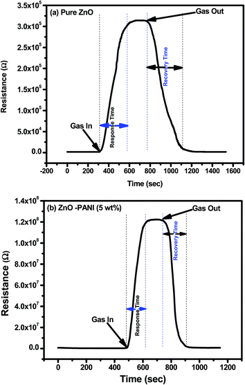
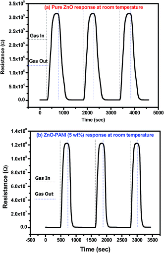
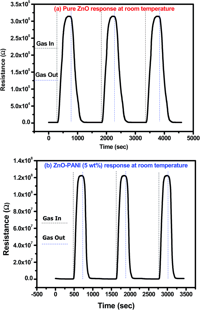
Fig. 7(a) and (b) show the transient response of pure ZnO and ZnO–PANI (5 wt%) composite thin film sensor at room temperature towards 20 ppm NO2 gas respectively. It can be observed from Fig. 7(a), that with the exposure of NO2 gas to the sensing film surface the sensor resistance increases from 1.83 kΩ to 311 kΩ (S = 170) and 196.86 kΩ to 120.58 MΩ (S = 611). The response time and recovery time of the sensor made of pure ZnO and ZnO–PANI (5 wt%) were observed to be 300 s, 350 s and 130 s, 170 s respectively.
 |
| | Fig. 7 Transient response of (a) pure ZnO and (b) ZnO–PANI (5 wt%) sensor towards 20 ppm of NO2 gas at room temperature. | |
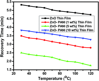
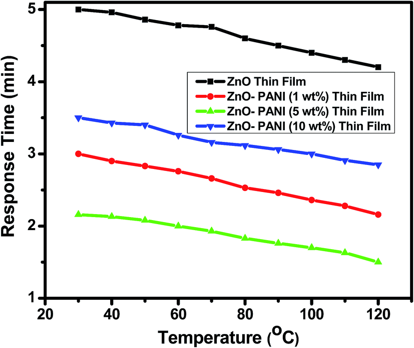
From Fig. 7 it is visualized that at room temperature, the pure ZnO thin film sensor gave response in 6 min while ZnO–PANI (1 wt%), ZnO–PANI (5 wt%) and ZnO–PANI (10 wt%) doped thin film sensor showed the response time of 3, 2.16 and 3.5 min towards 20 ppm NO2 gas respectively. Fig. 8 shows the variation of response time of pure ZnO, ZnO–PANI (1 wt%), ZnO–PANI (5 wt%) and ZnO–PANI (10 wt%) thin film sensors. Fig. 9 indicates the recovery time of ZnO–PANI (1 wt%), ZnO–PANI (5 wt%) and ZnO–PANI (10 wt%) thin film sensors, when NO2 gas was flushed out from the gas test chamber. From Fig. 8 it is clear that at room temperature, the recovery time of pure ZnO thin film is 5.33 min whereas ZnO–PANI (1 wt%), ZnO–PANI (5 wt%) and ZnO–PANI (10 wt%) thin films have the recovery times as 3.5, 2.5 and 3.8 min respectively. Furthermore, response and recovery times are seen to be reducing with temperature. This may be attributed to the fact that at room temperatures the rate of adsorption and desorption of gases increases. So, ZnO–PANI (5 wt%) doped thin film sensor is seen to be exhibiting better sensing properties compared to the other fabricated sensor structures. A brief summary of research work carried out on NO2 sensors is presented in Table 1. From table, it can be seen that the reported value of sensor response i.e. ∼611 is the highest amongst the previously reported literature.13,27–33
 |
| | Fig. 8 Variation in response time of the pure ZnO, ZnO–PANI (1 wt%), ZnO–PANI (5 wt%) and ZnO–PANI (10 wt%) thin film sensors. | |
 |
| | Fig. 9 Variation in recovery time of the pure ZnO, ZnO–PANI (1 wt%), ZnO–PANI (5 wt%) and ZnO–PANI (10 wt%) thin film sensors. | |
Table 1 A brief summary of research work carried out on NO2 sensors
| S. No. |
Materials |
Catalyst/modifier |
Gas conc. (ppm) |
Temp. (°C) |
Sensor response |
Resp. time (min) |
Recov. time (min) |
Ref. |
| 1 |
PANI |
— |
200 |
RT |
10 |
1.73 |
— |
27 |
| 2 |
ZnO |
— |
10 |
200 |
19 |
2 |
— |
28 |
| 3 |
ZnO |
— |
100 |
200 |
0.37 |
0.23 |
0.83 |
29 |
| 4 |
ZnO |
PPy |
100 |
RT |
0.38 |
4 |
— |
30 |
| 5 |
ZnO |
Cr |
5 |
100 |
63 |
0.5 |
1.16 |
31 |
| 6 |
SnO2–ZnO |
PANI |
35 |
180 |
368 |
0.46 |
— |
13 |
| 7 |
ZnO |
CuO |
29 |
350 |
9 |
1.66 |
2.16 |
32 |
| 8 |
WO3 |
PPy |
100 |
RT |
0.61 |
— |
— |
33 |
| 9 |
ZnO |
PANI |
20 |
RT |
611 |
2.16 |
3.50 |
Present work |
Fig. 10(a) and (b) show the reproducibility response of pure ZnO and ZnO–PANI (5 wt%) sensor structures, when continuously exposed to 20 ppm of NO2 gas and air for four consecutive cycles at room temperature. The sensor structures show the similar sensing response (Ra to Rg and Rg to Ra) repeatedly for four consecutive cycles towards 20 ppm NO2 gas and air which confirms the good reproducibility of the prepared sensor structure. The observed results show the good stability of the fabricated sensor in comparison to earlier reported sensors.
 |
| | Fig. 10 Transient response curve of repeated cycle towards 20 ppm of NO2 gas for (a) pure ZnO and (b) ZnO–PANI thin film sensor at room temperature. | |
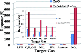
3.6 Selectivity of gas
The selectivity of sensing device made of ZnO, ZnO–PANI (1 wt%), ZnO–PANI (5 wt%), and ZnO–PANI (10 wt%) were investigated at room temperature by injecting 20 ppm NO2 and 1000 ppm concentration of other tested gases (LPG, C2H5OH, NH3, isopropyl alcohol and acetone). It was found that ZnO–PANI hybrid nanocomposite thin-film sensors with different PANI weight ratio could exhibit high sensitivity to NO2 but very low sensitivity to LPG, C2H5OH, NH3, IPA and acetone. Among all the above mentioned ZnO–PANI (1–5 wt%) hybrid nanocomposite thin film sensors, the sensor made of ZnO–PANI (5 wt%) hybrid nanocomposite thin-film exhibited the highest response of 611 to 20 ppm of NO2.
The selectivity of ZnO and ZnO–PANI (5 wt%) hybrid nanocomposite thin-film sensor is shown in bar diagram of Fig. 11. In order to study selectivity, 20 ppm of the test gases as NO2, LPG, C2H5OH, NH3, IPA and acetone were introduced in the test chamber and exposed to ZnO and ZnO–PANI (5 wt%) hybrid nanocomposite thin-film sensors. The responses of ZnO and ZnO–PANI (5 wt%) hybrid nanocomposite thin-film sensors to the NO2 gas (20 ppm) were 120 and 611, respectively, and least responses were observed for the other test gases.
 |
| | Fig. 11 Selectivity of ZnO and ZnO–PANI (5 wt%) for different tested gases as NO2, LPG, C2H5OH, NH3, IPA and acetone. | |
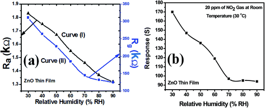
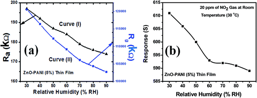
3.7 Effect of moisture on NO2 gas sensing
Curve (I) of Fig. 12(a) shows the variation in sensor resistance of ZnO thin film with increase in % RH before the exposure of NO2 gas and curve (II) of the same figure shows the variation in sensor resistance of ZnO thin film with increase in % RH after the exposure of NO2 gas. Similar behaviour can be observed through curve (I) and curve (II) for ZnO–PANI thin film with % RH before and after the exposure of NO2 gas at room temperature (30 °C). Fig. 12(b) and 13(b) show that the sensor response towards 20 ppm of NO2 gas decreases with increase in relative humidity (% RH) for ZnO and ZnO–PANI thin films at room temperature (30 °C). It was found that as % RH increases, the value of resistance decreases minutely; however, ZnO–PANI exhibited enhanced effect of moisture during the NO2 sensing.
 |
| | Fig. 12 (a) Variation of sensor resistance of ZnO thin film with relative humidity (% RH) and (b) sensor response with relative humidity (% RH) at room temperature (30 °C). | |
 |
| | Fig. 13 (a) Variation of sensor resistance of ZnO–PANI (5 wt%) thin film with relative humidity (% RH) and (b) sensor response with relative humidity (% RH) at room temperature (30 °C). | |
3.8 Gas sensing mechanism
Gas sensing of metaloxide sensors is based on the resistance change of the material due to the chemical and electronic interaction between the gas and sensing matrix. The chemical interaction involves the adsorption of the target gas molecules on the surface of ZnO thin film, where subsequent reaction with oxygen species adsorbed on the ZnO surface, results in the detection for the target gas.34,35
The adsorption and reaction process can be described as follows:
When ZnO sensor is exposed to air, oxygen molecules adsorb on the surface of the materials to form chemisorbed oxygen anions (O2(ads)−) by capturing electrons from the conductance band, resulting in the formation of a depletion layer, known as the space charge layer, on the surface of the sensor material which results in an increase in resistance of the material.
When the ZnO thin film is exposed to NO2 gas, it is adsorbed directly on the surface of ZnO thin film. Therefore, the concentration of electrons on the surface of ZnO thin film decreases and, correspondingly, the resistance of ZnO layer increases. The process of the reaction can be described as follows:
| | |
NO2(g) + e− ↔ NO2(ads)−
| (7) |
The above reactions result in the decrease of concentration of electron on the surface of ZnO which results in an increase in resistance of the material. In addition, following reaction is happened between NO2(ads)− and O(ads)−:
| | |
NO2(gas) + O2(ads)− + 2e− ↔ NO2(ads)− + 2O(ads)−
| (8) |
Thus the cyclic reaction continues as in eqn (7).
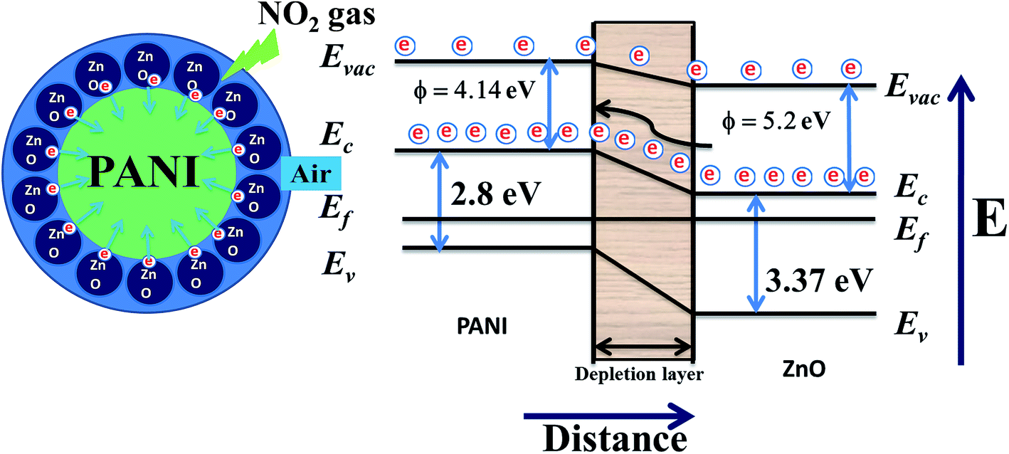
With the incorporation of p-type PANI29 into n-type ZnO,36 the sensing response towards NO2 gas was found to increase. This may be due to the formation of p–n junctions in the hybrid composite films and PANI chains are surrounded with mesh like structures made by ZnO nanoparticles. Here we are proposing a corresponding model for the ZnO–PANI heterojunction microstructures through the schematic shown by Fig. 14.
 |
| | Fig. 14 Schematic diagram of the proposed mechanism of NO2 sensing of ZnO/PANI heterojunctions. | |
During the formation of pn junction, minority charge carriers in PANI are lesser in number and they require lesser energy to move to conduction band as a result in beginning a small variation was observed but as the ZnO is n-type and excess in amount in the sample therefore, n-type nature of film will be dominating. Only the role of PANI will be to enhance the rate of reaction with oxidizing gas like NO2.
The first oxygen species were adsorbed on the surface of particles in the air, and then ionized into Oads− capturing free electron from the particles, thus leading to the formation of thin space charge layer and increasing of surface band bending. The doped PANI has a lower band gap and work function (Eg = 2.8 eV, ∅ = 4.14 eV) than that of ZnO (Eg = 3.37 eV, ∅ = 5.2 eV), the electrons are transferred towards the PANI, leading to the formation of an accumulation layer at the ZnO–PANI interface. After getting stabilized the film was exposed to NO2 and it is adsorbed by the heterojunctions between ZnO and PANI, NO2 acts as an electron acceptor in the reaction, and an acceptor surface state was occurred. As the surface state energy level is close to the valence band edge then to bring the Fermi level close to the surface state, the surface Fermi energy must be closed to the valence band. In such a situation, the acceptor surface state is so low in the band diagram that it extracts electrons from the valence band leaving a substantial hole concentration. As a result the lesser number of electrons are transferred from ZnO to PANI causing increase in the resistance.37 On the other hand, the trapped electrons are released to heterojunctions between ZnO and PANI by NO2 after stopping the supply of NO2, leading to a decrease of the resistance.
Further we want to submit that the improvement of sensing performances is attributed by tuning the structure of sensing materials through introduction of ZnO nanoparticles and PANI, and are the possible reasons for quick response and recovery time. Firstly, the ZnO nanoparticle not only tunes the surface active sites for adsorption and desorption of target gas, but also tunes the semiconducting properties. Secondly, the introduction of PANI could improve the electron transfer rate because of its better electrical conductivity.
Also we have calculated the activation energies for ZnO and ZnO–PANI nanocomposite by plotting the Arrhenius plots using eqn. 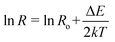 where ΔE, k and T are the activation energy, Boltzmann constant and absolute temperature of the film, respectively and found the values as 0.0025 and 0.0012 eV respectively. In the case of ZnO–PANI nanocomposite, activation energy is very low and may contribute for fast response at room ambient.
In the presence of NO2 the formation of an acceptor surface state was occurred. As the surface state energy level is closed to the valence band edge then to bring the Fermi level near to the surface state, the surface Fermi energy must be closed to the valence band. In such a situation the acceptor surface state is so low in the band diagram that it extracts electrons from the valence band leaving a substantial hole concentration. As a result the lesser number of electrons are transferred from ZnO to PANI causing increase in the resistance (Band model) Fig. 14.
4. Conclusion
The maximum sensing response ∼611 at room temperature towards 20 ppm of NO2 gas was obtained for ZnO–PANI (5%) hybrid composite sensor with a fast response and recovery times of about 2.16 min and 2.83 min respectively which is highest amongst the reported values by the previous researchers. However, the sensing responses as 170, 250 and 120 were obtained for bare ZnO, ZnO–PANI (1%) and ZnO–PANI (10%) sensor structures respectively towards 20 ppm of NO2 gas showing the importance of optimum concentration of PANI (5%) in the sensing layer of nanocomposite ZnO–PANI. Thus this sensor structure can be reliably used for the detection of NO2 gas at commercial level at room temperature.
Acknowledgements
Authors are thankful to Department of Science and Technology (DST), Department of Information Technology (DIT) and Gas Authority of India Pvt. Ltd. (GAIL). Govt. of India for the financial support for carrying out this research works. Mr R. K. Sonker is grateful to Babasaheb Bhimrao Ambedkar University, Lucknow for fellowship.
References
- H. S. Hwang and J. T. Song, J. Korean Phys. Soc., 2008, 53, 1384 CrossRef CAS
 .
. - R. L. N. Chandrakanthi and M. A. Careem, Thin Solid Films, 2002, 417, 51 CrossRef CAS .
- P. R. Somani, R. Marimuthu, U. P. Mulik, S. R. Mulik, S. R. Sanikar and D. P. Amalnerkar, Synth. Met., 1999, 106, 45 CrossRef CAS .
- Y. He, Mater. Chem. Phys., 2005, 92, 134 CrossRef CAS .
- O. Lupan, V. Cretu, M. Deng, D. Gedamu, I. Paulowicz, S. Kaps and Y. K. Mishra, J. Phys. Chem. C, 2014, 118, 15068 CAS .
- A. G. MacDiarmid, L. S. Yang, W. S. Huang and B. D. Humphrey, Synth. Met., 1987, 18, 393 CrossRef CAS .
- D. Verma and V. Datta, Sens. Actuators, B, 2008, 134, 373 CrossRef CAS .
- I. Paulowicz, V. Hrkac, S. Kaps, V. Cretu, O. Lupan, T. Braniste, V. Duppel and Y. K. Mishra, Adv. Electron. Mater., 2015, 1(8), 14 Search PubMed .
- R. K. Sonker and B. C. Yadav, Mater. Lett., 2015, 160, 581 CrossRef CAS .
- R. K. Sonker and B. C. Yadav, Adv. Sci. Lett., 2014, 20, 1023 CrossRef .
- R. K. Sonker, A. Sharma, M. Tomar, V. Gupta and B. C. Yadav, Adv. Sci. Lett., 2014, 20, 1374 CrossRef .
- B. C. Yadav, R. Srivastava, C. D. Dwivedi and P. Pramanik, Sens. Actuators, B, 2008, 131, 216 CrossRef CAS .
- M. Enachi, O. Lupan, T. Braniste, A. Sarua, L. Chow, Y. K. Mishra and D. Gedamu, Phys. Status Solidi RRL, 2015, 9, 171 CrossRef CAS .
- G. S. Devi, V. B. Subrahmanyam, S. C. Gadkari and S. K. Gupta, Anal. Chim. Acta, 2006, 30, 102 Search PubMed .
- H. Xu, X. Chen, J. Zhang, J. Wang, B. Cao and D. Cui, Sens. Actuators, B, 2013, 176, 166 CrossRef CAS .
- D. Gedamu, I. Paulowicz, S. Kaps, O. Lupan, S. Wille and G. Haidarschin, Adv. Mater., 2014, 26, 1541 CrossRef CAS PubMed .
- X. B. Yan, Z. J. Han, Y. Yang and B. K. Tay, Sens. Actuators, B, 2007, 123, 107 CrossRef CAS .
- R. K. Sonker, A. Sharma, Md. Shahabuddin, M. Tomar and V. Gupta, Adv. Mater. Lett., 2013, 4, 196 CAS .
- S. L. Patil, S. G. Pawar, A. T. Mane, M. A. Chougule and V. B. Patil, J. Mater. Sci.: Mater. Electron., 2010, 21, 1332 CrossRef CAS .
- G. Sarala Devi, V. B. Subrahmanyam, S. C. Gadkari and S. K. Gupta, Anal. Chim. Acta, 2006, 30, 102 Search PubMed .
- S. G. Pawar, S. L. Patil, M. A. Chougule, A. T. Mane, D. M. Jundale and V. B. Patil, Int. J. Polym. Mater., 2010, 59, 777 CrossRef CAS .
- R. K. Sonker, S. R. Sabhajeet, S. Singh and B. C. Yadav, Mater. Lett., 2015, 152, 189 CrossRef CAS .
- S. K. Shukla, N. B. Singh and R. P. Rastogi, Indian J. Eng. Mater. Sci., 2013, 20, 319 CAS .
- R. F. Silva and M. E. D. Zaniquelli, Colloids Surf., A, 2002, 198, 551 CrossRef .
- F. Ahmed, S. Kumar, N. Arshi, M. S. Anwar, L. S. Yeon, G. S. Kil, D. W. Park, B. H. Koo and C. G. Lee, Thin Solid Films, 2011, 519, 8375 CrossRef CAS .
- Y. He, Appl. Surf. Sci., 2005, 249, 1 CrossRef CAS .
- X. B. Yan, Z. J. Han, Y. Yang and B. K. Tay, Sens. Actuators, B, 2007, 123, 107 CrossRef CAS .
- S. Ozturk, N. Kılınc, N. Tasaltin and Z. Z. Ozturk, Thin Solid Films, 2011, 520, 932 CrossRef CAS .
- M. A. Chougule, S. Sen and V. B. Patil, Ceram. Int., 2012, 38, 2685 CrossRef CAS .
- M. A. Chougule, D. S. Dalavi, S. Mali, P. S. Patil, A. V. Moholkar and G. L. Agawane, et al., Measurement, 2012, 45, 1989 CrossRef .
- C. J. Chang, J. K. Chen and T. L. Yang, J. Taiwan Inst. Chem. Eng., 2014, 45, 1876 CrossRef CAS .
- L. Yang, C. Xie, G. Zhang, J. Zhao, X. Yu and D. Zeng, et al., Sens. Actuators, B, 2014, 195, 500 CrossRef CAS .
- A. T. Mane, S. T. Navale, S. Sen, D. K. Aswal, S. K. Gupta and V. B. Patil, Org. Electron., 2015, 16, 195 CrossRef CAS .
- S. L. Bai, L. Y. Chen, D. Q. Li, W. H. Yang, P. C. Yang, Z. Y. Liu, A. F. Chen and C. L. Chung, Sens. Actuators, B, 2010, 146, 129 CrossRef CAS .
- P. Rai, Y. S. Kim, H. M. Song, M. K. Song and Y. T. Yu, Sens. Actuators, B, 2012, 165, 133 CrossRef CAS .
- X. B. Yan, Z. J. Han, Y. Yang and B. K. Tay, Sens. Actuators, B, 2007, 123, 107 CrossRef CAS .
- S. Singh, B. C. Yadav, M. Singh and R. Kothari, Int. J. Sci. Tech. Soc., 2015, 1, 4 Search PubMed .
|
| This journal is © The Royal Society of Chemistry 2016 |


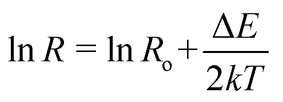 where ΔE, k and T are the activation energy, Boltzmann constant and absolute temperature of the film, respectively and found the values as 0.0025 and 0.0012 eV respectively. In the case of ZnO–PANI nanocomposite, activation energy is very low and may contribute for fast response at room ambient.