DOI:
10.1039/C5RA20928E
(Paper)
RSC Adv., 2016,
6, 1380-1387
Band gap modified boron doped NiO/Fe3O4 nanostructure as the positive electrode for high energy asymmetric supercapacitors†
Received
9th October 2015
, Accepted 7th December 2015
First published on 9th December 2015
Abstract
A boron doped NiO/Fe3O4 nanostructure was successfully synthesized by a facile one-step hydrothermal method. The boron doping was confirmed from the decreased band gap and increased electrical conductivity of the NiO/Fe3O4 composite. The Nyquist plot of the multimetal oxide was fitted with ZView software for detailed understanding of the effect of concentration of different metal oxides, boron doping and extensive charge–discharge cycles on the electrochemical properties of electrode materials. Very high specific capacitance of ∼1467 F g−1 was achieved as the synergistic effect of low activation energy and short ion diffusion path of the electrode materials. An asymmetric supercapacitor (ASS) was fabricated with the NiO/Fe3O4 composite and thermally reduced graphene oxide as the positive and negative electrode, respectively. The ASS showed a large specific capacitance of ∼377 F g−1 at a current density of 3 A g−1. Furthermore, the ASS showed a large energy density of ∼102.6 W h kg−1 and huge power density of ∼6300 W kg−1 and remained ∼82% stable even after 10![[thin space (1/6-em)]](https://www.rsc.org/images/entities/char_2009.gif) 000 charge–discharge cycles. Therefore, a facile hydrothermal method was demonstrated to enhance the electrochemical properties of a multimetal oxide by boron doping for the development of next generation energy storage devices.
000 charge–discharge cycles. Therefore, a facile hydrothermal method was demonstrated to enhance the electrochemical properties of a multimetal oxide by boron doping for the development of next generation energy storage devices.
1 Introduction
The development of a next-generation economical, flexible, light-weight and renewable energy storage system is strongly required to meet the future demand of portable and flexible electronics in modern society.1–3 In this realm, electrochemical supercapacitors (ESs) have received considerable attention as high-performance energy storage devices, since they can provide better capacitance, elevated power density, faster charge–discharge cycles, and long cycle life as compared to traditional lead-acid batteries or lithium-ion batteries.1,4,5 However, low energy density is the major limitation of the commercially available ESs.6–8 The use of an asymmetric configuration by utilizing both faradic and non-faradic charge storage mechanisms may be a green and nonhazardous solution to improving the operating voltage as well as the energy density of the ESs.4,9–12 Carbonaceous materials, such as carbon nanotubes, reduced graphene oxide (RGO) and CVD grown graphene, are the proper choice as the negative electrode materials in supercapacitor devices due to their electrochemical double layer capacitance (EDLC) charge storage mechanism.9,12,13 On the other hand, conductive polymers and different transition metal oxides/hydroxides with rich pseudo-capacitance are widely used as positive electrode materials to enlarge the operating voltage as well as the energy storage capacity.1,11,14
The fast redox reactions due to the surface faradic process at an appropriate potential is the origin of the pseudocapacitance.11 The small size and high surface area of the electrode materials effectively reduce the diffusion path of electrolyte ions, facilitating ionic motion and improving the pseudoactivity.11 The porous materials can simultaneously adsorb and retain electrolyte ions, resulting in good faradic reaction even in the high current density.15–17 However, the single-component nano-materials as electrodes show limitations due to the low electrical conductivity, rate capability and life stability.11,14,15 An efficient approach to increasing the rate capability of metal oxide/hydroxide positive electrode materials is to form a heterostructure by the incorporation of one or two metal ions into their lattices.11,15,16 The presence of a heterostructure creates an abundance of structural defects and multiple accessible electro-active sites, enhancing the redox reaction.11,16 Nano-structured binary Ni–Fe oxide is one of the most promising heterostructures for application in supercapacitors due to their large theoretical capacitance values, deep average discharging profiles and rich redox reactions.11,17,18 The interconversion between Fe(II) and Fe(III) provides the redox capacitance for Fe3O4 in an aqueous electrolyte.18 NiO contributes to the pseudocapacitance based on the surface reversible redox mechanism.17
NiO and Fe3O4 are semiconducting materials with band gap energy of 3.6–4 eV and 1.92–2.87 eV, respectively.19,20 The heterostructure of two different metal oxides is advantageous due to the size confinement of the highly enhanced electron–electron interactions.21 The creation of defects or dislocations is highly expected due to the different lattice structures of the participating semiconductors, which can create localized states by trapping the charge carriers and control the overall electrical characteristics of the system.22 Furthermore, quantum interference effects can be reduced between the thin layers of the semiconducting heterostructure, allowing enhanced ion exchange at the grain boundary.22 The energy separation of the two different band structures can create a barrier, and as a result the charge carriers can be confined, allowing a quasi-equilibrium potential state within the electrode.12,22
However, the large band gap or high electrical resistivity of NiO limits its applications. Therefore, superior electrochemical activity requires control of the electrical properties through proper doping of the materials.12,23–26 In addition, controlled doping significantly increases the carrier concentration by creating free charge carriers.25 Saha et al. showed that the band gap modification of insulating boron nitride is highly effective for electrochemical or supercapacitor applications.12 Alver et al. explained the effect of boron doping on the band structure and electrical conductivity of NiO.25 Chi et al. showed that the supercapacitor performance of MnO2 increases after boron doping.26
On the basis of the abovementioned considerations, a one-step hydrothermal synthesis of a boron doped NiO/Fe3O4 nanocomposite has been demonstrated. Nickel sulphate, iron sulphate and boric acid were used as the source of nickel, iron and boron, respectively. The electrical conductivity of the NiO/Fe3O4 nanocomposite increases significantly due to the boron doping. The variation in the morphology of the composite can be observed with different ratios of nickel sulphate and iron sulphate precursor. Furthermore, the supercapacitive performance varied with the morphology of the nanostructure, and better results were obtained after boron doping. The asymmetric supercapacitor (ASS) cell was designed and fabricated using the NiO/Fe3O4 composite as the positive and thermally reduced graphene oxide (TRGO) as the negative electrode materials.
2 Experimental
2.1 Reagents
Natural graphite flakes were purchased from Sigma-Aldrich. Hydrochloric acid, sulphuric acid, potassium permanganate, hydrogen peroxide, nickel sulphate, iron sulphate, boric acid, ammonia solution, N,N-dimethylformamide (DMF) and potassium hydroxide were purchased from Merck, Mumbai, India. Conducting carbon black (EC-600JD, purity: >95%) and polyvinylidene fluoride (PVDF) were purchased from Akzo Nobel Amides Co., Ltd, South Korea. Nickel foam was purchased from Shanghai Winfay New Material Co., Ltd, China.
2.2 Preparation of boron doped NiO/Fe3O4 composites and TRGO
NiSO4 (∼2 g) and FeSO4 (∼2 g) were dissolved in ∼60 ml of distilled water. The solution was taken in a 100 ml Teflon lined autoclave. About 20 ml of ammonia solution was added, and the autoclave was maintained at 160 °C for 5 h. The product was collected by vacuum filtration (with distilled water and ethanol) and dried inside a vacuum oven at 50 °C. The sample was designated as FN. Another two samples, F1N2 and F2N1, were prepared by varying the concentration of NiSO4 and FeSO4. About 2 g of NiSO4 and 1 g of FeSO4 were taken for the preparation of F1N2. Similarly, about 1 g of NiSO4 and 2 g of FeSO4 were taken for the preparation of F2N1. F1N2B was prepared by adding 0.5 g of boric acid to the autoclave while keeping the other parameters constant (same as that of F1N2). Another three samples, F1N2B1, F1N2B2 and F1N2B3, were prepared by increasing the concentration of boric acid. About 1, 1.5 and 2 g of boric acid was used for F1N2B1, F1N2B2 and F1N2B3, respectively, keeping other parameters constant. GO was prepared from natural graphite flake by the modified Hummers' method.12 Thermally reduced GO (TRGO) was prepared through the thermal reduction of GO (∼100 mg) at 500 °C for ∼15 min (under Ar gas atmosphere).
2.3 Structural and morphological characterization
X-ray diffraction (XRD) studies of the composite were carried out at room temperature on a D/Max 2500 V/PC (Rigaku Corporation, Tokyo, Japan) at a scan rate of 1° min−1 (Cu Kα radiation, λ = 0.15418 nm). The morphology of the NiO/Fe3O4 was measured by field emission scanning electron microscopy (FE-SEM) using a Σigma HD (Carl Zeiss, Germany), and transmission electron microscopy (TEM) was carried out using a JEOLTEM 2100 FS instrument (Japan) at 200 kV. X-ray photoelectron spectroscopy (XPS) was carried out using a K-alpha X-ray photoelectron spectrometer, Thermal scientific TM.
2.4 Optical, electrical and electrochemical properties
UV-vis spectroscopy was performed on an Agilent Cary 60 spectrophotometer. Band gap was calculated according to the Tauc relationship: αhν = B(hν − Eg)n, where α is the absorption coefficient, hν is the energy of a photon, B is a proportionality constant, Eg represents the optical band gap, and n is the parameter of specific electronic transition within the band due to the light absorption (n = 1/2 or 2 for direct or indirect transition, respectively).12,19,27
The electrical conductivity (σ) was measured using a four probe set up with a KEITHLEY delta system consisting of an AC and DC current source (model: 6221) and a Nanovoltmeter (model: 2182A) following the formula:  , where ρ is the resistivity of the material. R and d are the resistance and thickness of the prepared pellet.12,18,28 The high and low current ranges during the measurement were recorded in the range from 20 × 10−6 to −20 × 10−6 A, and the delta voltage step was fixed at 100 mV s−1 for all the samples. The electrochemical properties were recorded with a PARSTAT 4000 (Princeton Applied Research, USA) electrochemical workstation using 1 M Na2SO4 as the electrolyte. Specific capacitance was calculated from the CV curves using the equation: CCV = (∫IdV)/mυ, where CCV is the specific capacitance (F g−1), I is the response current density (A g−2), V is the potential window, υ is the scan rate (mV s−1), and m is the deposited mass on the electrode.12,29–31 The specific capacitance can be calculated in terms of the discharge time according to the equation: CCD = IΔt/mV, where CCD is the specific capacitance (F g−1), I is the discharging current (A g−1), V is the potential window (V) and m is the deposited mass on the electrode.12,30,31 The mass balance of the electrodes for asymmetric configuration was done according to the relation:
  , where m+ and m− are the mass of the positive and negative electrodes, C+ and ΔE+ are the specific capacitance and potential window (calculated from the three electrode measurement) for the positive electrode, and C− and ΔE− are the specific capacitance and potential window of the negative electrode measured at the same scan rate.12,32,33 The energy density (ED) and power density (PD) can be calculated according to the formula, ED = CV2/2 and PD = ED/ΔT, where C is the specific capacitance, V is the operating voltage, and ΔT is the discharge time.12,33,34
3 Results and discussion
The formation of NiO and Fe3O4 can be explained by the following reaction mechanism:
| Ni2+ + 2NH3 + 2H2O ↔ Ni(OH)2 + 2NH4+ |
| Fe2+ + 3NH3 + 3H2O ↔ Fe(OH)3 + 3NH4+ |
Nickel hydroxide and iron hydroxides were formed in the presence of NiSO4, FeSO4 and aqueous ammonia solution. However, the hydrothermal process involves high temperature and pressure, which results in the formation of multimetal oxides of iron and nickel. The hydrothermal reaction was carried out only for 5 h to avoid the formation of the spinel phase rather than the single phase metal oxide composite. Extended duration of the hydrothermal reaction or high temperature annealing can result in the formation of the spinel phase. Fig. S1 of the ESI† represents the XRD pattern of F1N2, FN and F2N1. The peaks corresponding to both cubic NiO and Fe3O4 are present in all three composites.17–20 The relative intensity of the NiO peaks as compared to Fe3O4 increased with increasing concentration of NiSO4 in the precursor. The amount of NiO in comparison to Fe3O4 increased from F2N1 to FN to F1N2. FE-SEM image analysis was carried out for the detailed morphological study of the multimetal composites. The FE-SEM images show that the concentration of nickel oxide plays an important role in the morphology of the composite. Fig. 1a–c represent the low resolution FE-SEM images of F1N2, FN and F2N1. The composite has a cactus-like porous structure with higher concentration of NiO (F1N2). The cactus-like structure started to distort with increasing concentration of Fe3O4 (FN) and was completely destroyed for F2N1. Fig. S2a–c of the ESI† represent the high magnifying FE-SEM images of F1N2, FN and F2N1. The Fe3O4 particles are totally embedded in the NiO structure for F1N2. The increase in particle size and a quite inhomogeneous particle size distribution of NiO and Fe3O4 was noticed in FN. The arbitrarily distributed Fe3O4 and NiO particles of F2N1 can be seen from Fig. 1c.
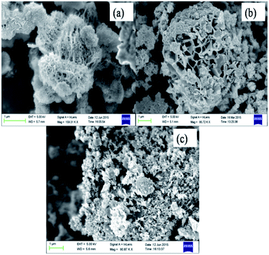 |
| | Fig. 1 Low resolution FE-SEM image of (a) F1N2, (b) FN and (c) F2N1. | |
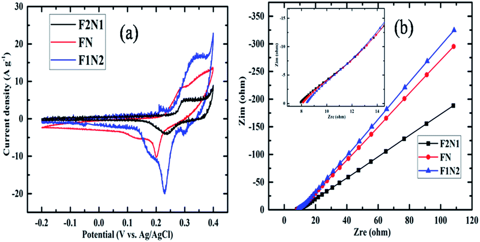
Fig. 2a shows the comparison of the three electrode CVs of F1N2, FN and F2N1. The increase in the current response was noticed with increasing concentration of NiO. The maximum specific capacitance of F2N1, FN and F1N2 was calculated as 500, 583 and 666 F g−1, respectively. The increase in specific capacitance with increasing NiO was explained by the Nyquist plot analysis. Fig. 2b shows the Nyquist plots of F1N2, FN and F2N1. The solution resistance of the composites were comparatively large. The low electrical conductivity of metal oxides may be the reason for such high solution resistance. The slight increase in solution resistance was noticed with the increase of NiO concentration in the composite. The inclination of the Warburg region towards the imaginary axis represented good electrolyte accessibility due to the porous materials or fascinating diffusion path. The FE-SEM images showed that the particle size of the NiO/Fe3O4 composites decreased with increasing NiO concentration. It was expected that the surface area of the composite would increase with decreasing particle size. The Nyquist analysis also showed a steeper Warburg region for the composites with higher content of NiO.18,35 The slope of the Warburg region was very low for the F2N, indicating poor porosity as well as low capacitance value. The supercapacitor performance of solo NiO and Fe3O4 was tested and compared with that of the NiO/Fe3O4 composite, as shown in Fig. S3 of the ESI.† The current responses of the solo metal oxides were poor compared to that of the NiO/Fe3O4 composite. The specific capacitance was calculated at a scan rate of 10 mV s−1, and the results showed a prominent increase in specific capacitance for the composite (583 F g−1). The specific capacitances of solo NiO and Fe3O4 were found to be 143 and 294 F g−1, respectively.
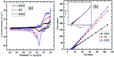 |
| | Fig. 2 (a) CV and (b) EIS of F1N1, FN and F2N1. | |
Fig. S4 of the ESI† shows the CV plots of F1N2, FN and F2N1. The current response of CV increased for all three composites. The retention of the specific capacitance of the composites has been compared in Fig. S5 of the ESI.† The retention is very low for F2N1 and increased with NiO concentration. The good capacitance value may be attributed to the synergistic effect of faradic reactions from NiO and Fe3O4. However, the capacitance value was quite low compared to the theoretical value, and the retention is only about ∼52% at a scan rate of 200 mV s−1. On the basis of the abovementioned discussion, F1N2 was the best composite for supercapacitor application, and the electrical/electrochemical properties of F1N2 were further improved by boron doping.
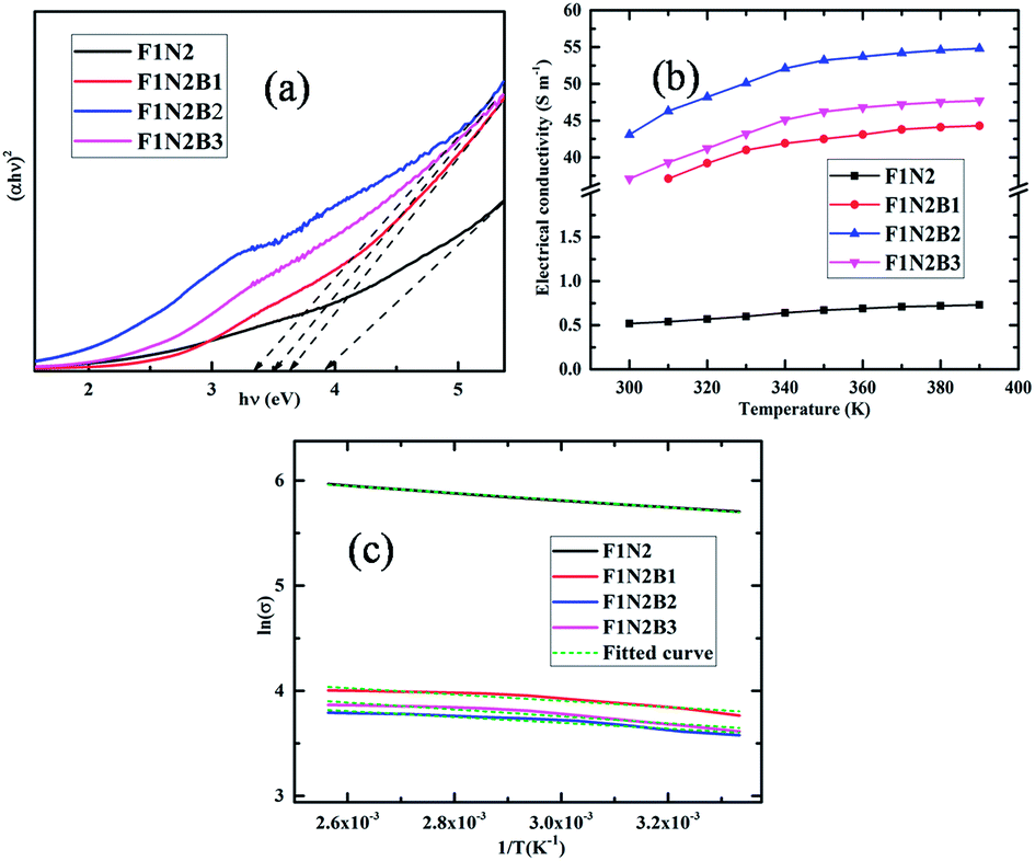
UV-visible absorption spectroscopy of F1N2 and its boron doped composites was carried out to visualize the effect of boron on the electronic properties of the multimetal oxide (Fig. S6 of ESI†). Significant increase in absorbance intensity was noticed with the insertion of boron (for F1N2B1). The absorbance increased for F1N2B2 from that of F1N2B1, but the intensity decreased with further doping. The (αhν)2 vs. hν plots of F1N2 and the boron doped composites are shown in Fig. 3a. The band gap can be directly calculated from the intersection of the slope to the X-axis.12,19,27 F1N2 showed a wide band gap of 3.93 eV. Boron doping significantly reduced the band gap of the multimetal oxide. The calculated band gaps of F1N2B1 and F1N2B2 were 3.63 and 3.31 eV, respectively. The band gap was increased further in F1N2B3 (3.41 eV) due to B doping into the lattice. The variation of the optical band gap values of the multimetal composites can be attributed to the creation of linear and/or planar defects due to the boron doping in the crystal structure.23,25 The doping of boron produced free electrons in the conduction band of the multimetal oxide heterostructure, resulting in the decrease in band gap energy. The increase in band gap energy with the higher concentration of boron was ascribed to the excess doping over the optimum level. The Fermi level increased with increasing doping concentration and thus free electrons, resulting in the shifting of the absorption edge to higher energy.36 This phenomenon is called the Burstein–Moss effect.36 The electrical conductivity increased abruptly due to boron doping. The variation of electrical conductivity of F1N2 and the boron doped composites are shown in Fig. 3b. The un-doped F1N2 showed a very low electrical conductivity of 0.52 S m−1 at room temperature. The electrical conductivity of the multimetal oxide was enhanced by ∼50 times with B doping. F1N2B1 and F1N2B2 displayed the electrical conductivity of 25.8 and 43.1 S m−1, respectively, at room temperature. Decrease in electrical conductivity (37.1 S m−1) was noticed for F1N2B3 after further doping. The decrease in electrical conductivity of F1N2B3 may be attributed to the poor carrier mobility at very high concentration of boron.25 The electrical conductivity increased with temperature for all the composites, indicating pure semiconducting natures. Fig. 3c shows the linear fitted plot of ln(σ) vs. 1/T. The activation energy was calculated from the slope of the linear fit.12,37,38 The activation energy of F2N1, F1N2, F1N2B1 and F1N2B2 were 0.29, 0.279, 0.232 and 0.255 eV, respectively. The Nyquist analysis was carried out for proper understanding of the effect of surface morphology, boron doping and increased electrical conductivity on the electrochemical properties of the multimetal oxides.
 |
| | Fig. 3 (a) (αhν)2 vs. hν plot, (b) variation of electrical conductivity with temperature and (c) Arrhenius plot of F1N2, F1N2B1, F1N2B2 and F1N2B3. | |
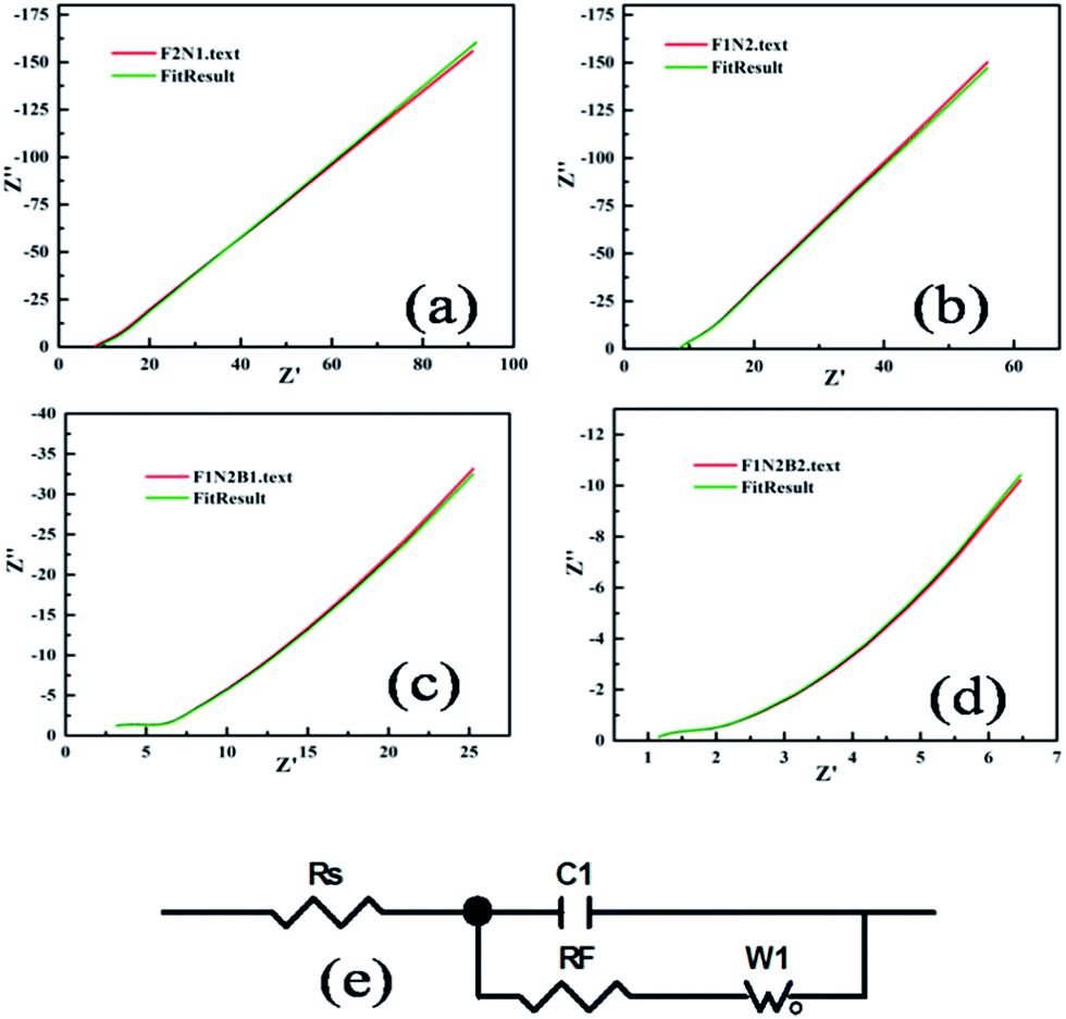
The Nyquist result was fitted with ZView software to find out the effect of boron doping on the diffusion path and the diffusion resistance. A perfect semicircle of the Nyquist plot is obtained for an electrode involving only the EDLC mechanism.12,18,39 A Warburg region results from a pseudoreaction.12,18,37 Fig. 4 shows the ZView fitted results of F2N1, F1N2, F1N2B1 and F1N2B2. The Warburg impedance (W) represents the route of ion diffusion between the electrode and electrolyte interfaces. W contains three parts: ohmic resistance (W-R), diffusion time constant (W-T), and Warburg exponent (W-P).34,40–42 The origin of the solution resistance is the electrode and electrolyte contact, and it depends on the electrical conductivity of the electrode materials.12,34 Table 1 shows the ZView fitted result of F2N1, F1N2, F1N2B1 and F1N2B2. Both F2N1 and F1N2 were undoped composites, and no significant variation of solution and faradic resistance were noticed. The solution resistance decreased significantly with the insertion of boron. The solution resistance of F2N1, F1N2, F1N2B1 and F1N2B2 were 9.6, 9.4, 5.2 and 1.4 Ω, respectively. The decrease in solution resistance may be attributed to the generation of free electrons and increased electrical conductivity of the boron doped composites. The faradic resistance also decreased after boron doping. The diffusion path as well as the diffusion time is an important parameter for an electrode material for enriched supercapacitor performance.39
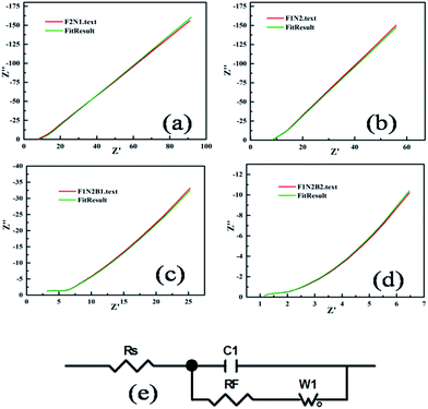 |
| | Fig. 4 ZView fitted Nyquist plots of (a) F2N1, (b) F1N2, (c) F1N2B1 and (d) F1N2B2. (e) Corresponding equivalent circuit. | |
Table 1 ZView fitted result of F2N1, F1N2, F1N2B1 and F1N2B2
| |
Rs |
RF |
W-R |
W-T |
| F2N1 |
9.6 |
3.9 |
55.9 |
0.0068 |
| F1N2 |
9.4 |
3.9 |
18.9 |
0.0048 |
| F1N2B1 |
5.2 |
0.3 |
5.7 |
0.0037 |
| F1N2B2 |
1.4 |
0.29 |
1.9 |
0.0022 |
The diffusion current constant is directly related to the diffusion path.39 The diffusion current constant of F2N1 and F1N2 are 0.0068 and 0.0048, respectively. The decrease in diffusion path may be attributed to the synergistic effect of high surface area and better incorporation of NiO and Fe3O4 particles in F1N2. The diffusion current constant further decreased after boron doping. The low diffusion time constant of F1N2B1 as compared to that of F1N2 may be attributed to the creation of huge defect sites and free electrons after boron doping. The formation of free electrons elevated the diffusion of charge carriers in the multimetal oxide. The low W-R value of F1N2B1 as compared to that of F1N2 also supported the formation of a shorter ion diffusion path.18,35 The low Warburg resistance and diffusion time constant are possibly attributed to the decrease in activation energy of the multimetal oxide. The Arrhenius equation plays a governing role in the chemical kinetics.38 The diffusion rate is related to the activation energy and lattice parameter of the material. The correlation between the activation energy and electrochemical diffusion has been explained elaborately in the ESI.† The decrease in activation energy of the multimetal composite after boron doping indicated the enhanced ion diffusion through electrode materials.38 Furthermore, the Warburg resistance arises from ionic blocking at the interface of the grain boundary of the electrode materials.38 The simultaneous decrease in activation energy and W-R suggested enhanced ionic exchange at the interface of the metal oxide grain boundary as the synergistic effect of increasing concentration of NiO and boron doping. The FE-SEM and TEM images of F1N2B2 show that the morphology of the composite remained undistorted after boron doping (Fig. S7a and b of the ESI†). The extensive increase in current response of the multimetal oxide was noticed after modification of the band gap by boron doping (Fig. 5a). The specific capacitance of F1N2, F1N2B1 and F1N2B2 at 10 mV s−1 scan rate was measured as 1184, 1467 and 1293 F g−1, respectively. The successive increase and decrease in specific capacitance with different concentrations of boron doping shows consistency with the band gap and electrical conductivity analysis.
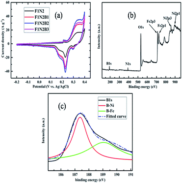 |
| | Fig. 5 (a) CV plot of F1N2, F1N2B1, F1N2B2 and F1N2B3. (b) XPS survey plot of F1N2B2 and (c) B1s spectrum of F1N2B2. | |
The CD plot shows the F1N2B2 has IR drop from 0.4 to 0.3 V (Fig. S8a of the ESI†). The maximum specific capacitance of 1305 F g−1 was achieved at a current density of 3.5 A g−1. F1N2B2 showed ∼70% retention in specific capacitance at a high current density of 8 A g−1 (Fig. S8b of the ESI†). Fig. 5b shows the XPS survey spectra of F1N2B2. The peaks at 711, 724.5, 855.6 and 873.1 eV were attributed to the Fe 2p3/2, Fe 2p1/2, Ni 2p3/2 and Ni 2p1/2, respectively.18,43 The Ni 2p3/2 peak position was different from that of metallic Ni (852.7 eV). The energy difference between Ni 2p3/2 and Ni 2p1/2 core levels (∼17.5 eV) was also different from that of metallic Ni (17.27 eV).43 The positive shift and the increase in the core level energy difference may be attributed to the +2 valence state of Ni in NiO.43 The B1s peak appeared at 187.3 eV. The positive shift of the elemental B1s peak as compared to that of pure B (187.1 eV) indicates that boron donated its partial electron to the alloying metals.44 Fig. 5c shows the high resolution B1s spectra of F1N2B2. The B1s spectra were deconvoluted in two separate peaks. The peaks at 187.2 and 189.1 eV may be attributed to B–Ni and B–Fe, respectively.45,46 The most intense peak of B–Ni indicates that the bond formation between B and Ni was greater compared to that of B–Fe. The B doping ratio was estimated from the XPS peak table analysis. The atomic percentage of boron was calculated as 6.13%, 9.71% and 10.6% for F1N2B1, F1N2B2 and F1N2B3, respectively.
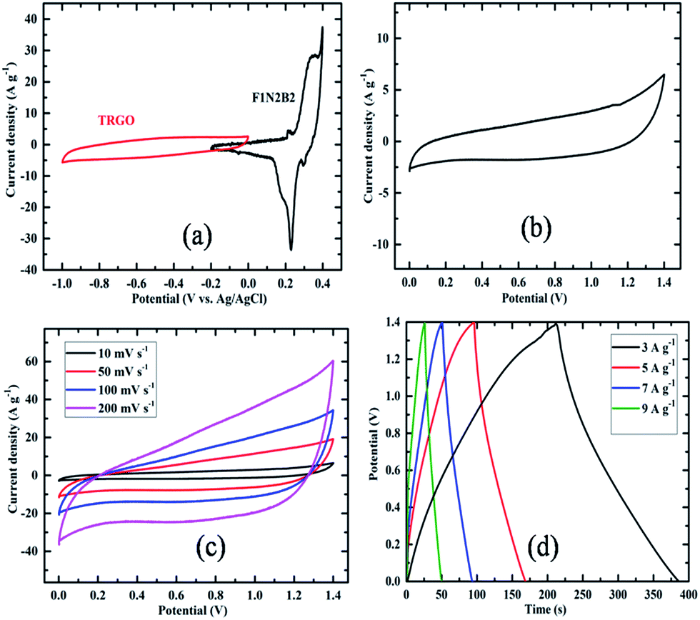
The specific capacitance of the multimetal oxide composite increased appreciably after boron doping but still suffered from an IR drop of ∼0.1 V and a small potential window. The asymmetric cell was designed to overcome these limitations. TRGO was used as the negative electrode, and the mass deposition ratio of TRGO to F1N2B2 was 1:52. The CVs of TRGO, FIN2B2 and ASS have been compared in Fig. 6a and b. The CV of ASS at different scan rates is shown in Fig. 6c. The CV nature was nearly rectangular and remained undistorted at the higher scan rates. The CD was carried out with different current densities from 3 to 9 A g−1, and the discharging profile of the CD shows almost zero IR drop. The maximum specific capacitance calculated from the CV was 390 F g−1 at a scan rate of 10 mV s−1, and the ASS showed good capacitance retention of ∼60% at a very high scan rate of 200 mV s−1 (Fig. S9a of ESI†). The capacitive performance of ASS was studied from the discharging time, as shown in Fig. S9b of the ESI.† The ASS exhibited a specific capacitance of 377 and 157 F g−1 at a current density of 3 and 9 A g−1, respectively.
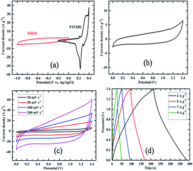 |
| | Fig. 6 (a) Comparison of three electrode CV of F1N2B2 and TRGO, (b) CV of ASS, (c) CV of ASS at different scan rates and (d) CD of ASS at different current densities. | |
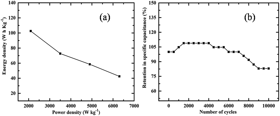
Fig. 7a shows the Ragone plot of the ASS cell. The large potential window and high specific capacitance value of the ASS cell provided a very high energy density of 102.6 W h kg−1. Furthermore, the ASS was able to deliver a huge power density of ∼6300 W kg−1. The stability of the ASS cell was tested up to 10000 cycles. The initial increase in specific capacitance from 500 to 1500 cycles (108%) may be attributed to the wetting of the electrolyte and enhanced electrode electrolyte contact. The ASS was 100% stable up to 7000 cycles. The stability decreased to ∼82% after 9000 CD cycles and remained constant over 10000 cycles. The degradation of the electrolyte may be the reason for the deteriorated capacitance.
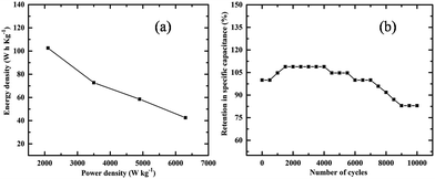 |
| | Fig. 7 (a) Ragone plot and (b) stability plot of ASS. | |
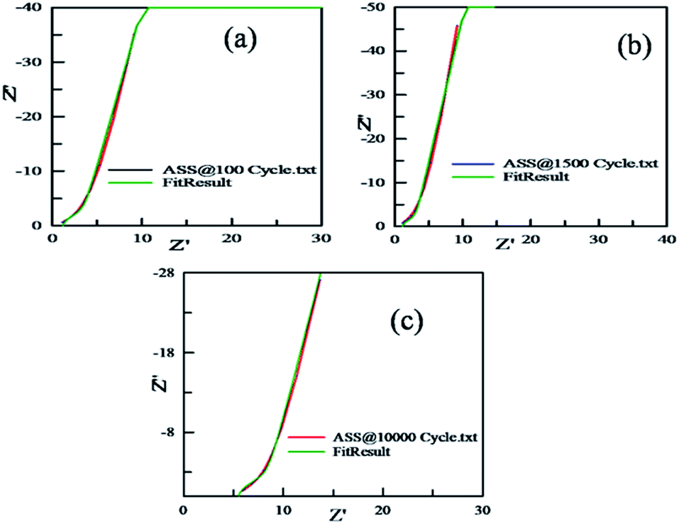
The Nyquist results of the ASS after 100, 1500 and 10000 CD cycles were fitted with ZView for detailed understanding of the variation of capacitance during the stability test (Fig. 8). The ZView fitted results are summarized in Table 2. The ASS showed a very low solution resistance of ∼1.2 ohms and almost zero faradic resistance during the initial cycles. These parameters remained unchanged after 1500 cycles. The increased specific capacitance of ASS after 1500 cycles was attributed to the improved Warburg impedance. The wetting of the electrode materials decreased the diffusion time constant and Warburg resistance, allowing good ion exchange between the electrode materials and electrolyte. The solution and faradic resistance increased after 10000 cycles possibly due to the degradation of the electrolyte. The increase in the diffusion time constant indicated the relatively poor ion exchange between the electrode materials and electrolyte after 10000 cycles.
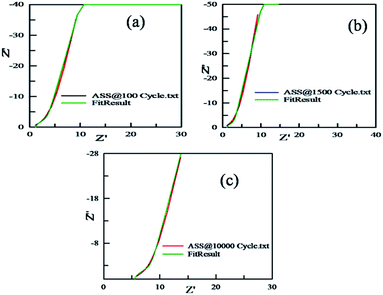 |
| | Fig. 8 ZView fitted Nyquist plot of ASS after (a) 100, (b) 1500 and (c) 10000 CD cycles. | |
Table 2 ZView fitted result of ASS@100 cycle, ASS@1500 cycle and ASS@10000 cycle
| |
Rs |
RF |
W-R |
W-T |
| ASS@100 cycle |
1.2 |
0.2 |
9.9 |
0.019 |
| ASS@1500 cycle |
1.1 |
0.2 |
7.5 |
0.017 |
| ASS@10000 cycle |
5.5 |
0.5 |
9.9 |
0.039 |
4 Conclusions
Boron doped NiO/Fe3O4 was successfully synthesized through a simple one-step hydrothermal method. Increasing the concentration of NiO decreased the particle size, and the Warburg resistance decreased due to the increased ionic conductivity at the grain boundary of the multimetal oxide. The large band gap between the metal oxides was decreased by boron doping. The optimized doping created defects in the multimetal structure to generate large numbers of free electrons. The electrical conductivity increased significantly after boron doping. The synergistic effect of enhanced electrical conductivity and lower activation energy was observed at the lower frequency region of the Nyquist plot. The ZView fitted results showed that the effective diffusion path of the electrode materials decreased after increasing the concentration of NiO. The short ion diffusion path and decreased solution resistance that enhanced the specific capacitance of the multimetal oxide were results of boron doping. A very high specific capacitance of 1305 F g−1 was achieved at a current density of 3.5 A g−1. However, the F1N2B2 suffered from a large IR drop and comparatively low rate capability. The ASS cell was developed with TRGO as the negative electrode material, and the CD plot of the ASS showed almost zero IR drop. The ASS exhibited good rate capability and a large specific capacitance of 377 F g−1 at a current density of 3 A g−1. The ASS remained ∼82% stable even after 10000 CD cycles tested at a high current density of 9 A g−1. Furthermore, the large energy density of 102.6 W h kg−1 and huge power density of ∼6300 W kg−1 ensure that boron doped NiO/Fe3O4 is a potential electrode material for new generation energy storage devices.
Acknowledgements
Authors (a and b) are thankful to the Director of CSIR-CMERI. Authors are also thankful to the Department of Science and Technology, New Delhi, India, for the financial support from the DST-INSPIRE Faculty Scheme-INSPIRE Programme (IFA12CH-47) and Council of Scientific and Industrial Research, New Delhi, India, for funding MEGA Institutional project (ESC0112/RP-II). Authors (c and d) would also like to acknowledge the financial support from the R&D Convergence Program of MSIP (Ministry of Science, ICT and Future Planning) of Republic of Korea (Grant CAP-13-2-ETRI).
Notes and references
- X. Hu, W. Zhang, X. Liu, Y. Mei and Y. Huang, Chem. Soc. Rev., 2015, 44, 2376–2404 RSC.
- I. Shown, A. Ganguly, L. C. Chen and K. H. Chen, Energy Sci. Eng., 2015, 3, 2–26 CrossRef CAS.
- J. D. Lipomi and Z. Bao, Energy Environ. Sci., 2011, 4, 3314–3328 Search PubMed.
- S. Gao, Y. Sun, F. Lei, L. Liang, J. Liu, W. Bi, B. Pan and Y. Xie, Angew. Chem., Int. Ed., 2014, 53, 12789–12793 CrossRef CAS PubMed.
- W. Jiang, D. Yu, Q. Zhang, K. Goh, L. Wei, Y. Yong, R. Jian, J. Wei and Y. Chen, Adv. Funct. Mater., 2015, 25, 1063–1073 CrossRef CAS.
- B. Senthilkumar, Z. Khan, S. Park, K. Kim, H. Ko and Y. Kim, J. Mater. Chem. A, 2015, 3, 21553–21561 CAS.
- L. Li, S. Peng, H. B. Wu, L. Yu, S. Madhavi and X. W. Lou, Adv. Energy Mater., 2015, 5, 1500753–1500758 Search PubMed.
- S. Dong, L. Shen, H. Li, P. Nie, Y. Zhu, Q. Sheng and X. Zhang, J. Mater. Chem. A, 2015, 3, 21277–21283 CAS.
- H. Xia, C. Hong, B. Li, B. Zhao, Z. Lin, M. Zheng, V. S. Savilov and S. M. Aldoshin, Adv. Funct. Mater., 2015, 25, 627–635 CrossRef CAS.
- Y. Yang, L. Li, G. Ruan, H. Fei, C. Xiang, X. Fan and J. M. Tour, ACS Nano, 2014, 8, 9622–9628 CrossRef CAS PubMed.
- R. Wang and X. Yan, Sci. Rep., 2014, 4, 3712 Search PubMed.
- S. Saha, M. Jana, P. Khanra, P. Samanta, H. Koo, N. C. Murmu and T. Kuila, ACS Appl. Mater. Interfaces, 2015, 7, 14211–14222 CAS.
- C. Yang, J. Shen, C. Wang, H. Fei, H. Bao and G. Wang, J. Mater. Chem. A, 2014, 2, 1458–1464 CAS.
- R. Zou, F. M. Yuen, Z. Zhang, J. Hu and W. Zhang, J. Mater. Chem. A, 2015, 3, 1717–1723 CAS.
- D. Sarkar, G. G. Khan, A. K. Singh and K. Mandal, J. Phys. Chem. C, 2013, 117, 15523–15531 CAS.
- P. D. Dubal, D. Aradilla, G. Bidan, P. Gentile, S. T. J. Schubert, J. Wimberg, S. Sadki and G. P. Romero, Sci. Rep., 2015, 5, 09771 CrossRef PubMed.
- B. Zhao, J. Song, P. Liu, W. Xu, T. Fang, Z. Jiao, H. Zhang and Y. Jiang, J. Mater. Chem., 2011, 21, 18792–18798 RSC.
- S. Saha, M. Jana, P. Samanta, N. C. Murmu, N. H. Kim, T. Kuila and J. H. Lee, RSC Adv., 2014, 4, 44777–44785 RSC.
- K. Anandan and V. Rajendran, International Journal of NanoScience and Nanotechnology, 2012, 2, 24–29 Search PubMed.
- H. E. Ghandoor, H. M. Zidan, M. M. H. Khalil and M. I. M. Ismail, Int. J. Electrochem. Sci., 2012, 7, 5734–5745 Search PubMed.
- X. Hong, J. Kim, S. F. Shi, Y. Zhang, C. Jin, Y. Sun, S. Tongay, J. Wu, Y. Zhang and F. Wang, Nat. Nanotechnol., 2014, 9, 167 CrossRef PubMed.
- W. R. Frensley, A volume of VLSI electronics: microstructure science, San Diego, 1994, pp. 1–28 Search PubMed.
- K. W. Noh, Defect engineering of metal oxide semiconductors, University of Illinois at Urbana-Champaign, Urbana, Illinois, 2010 Search PubMed.
- P. Nguyen, H. T. Ng, J. Kong, A. M. Cassell, R. Quinn, J. Li, J. Han and M. McNeil, Nano Lett., 2003, 3, 925–928 CrossRef CAS.
- U. Alver, H. Yaykash, S. Kerli and A. Tanrıverdi, Int. J. Miner., Metall. Mater., 2013, 20, 1097–1101 CrossRef CAS.
- H. Z. Chi, Y. Li, Y. Xin and H. Qin, Chem. Commun., 2014, 50, 13349–13352 RSC.
- G. Gao, W. Gao, E. Cannuccia, J. T. Tijerina, L. Balicas, A. Mathkar, T. N. Narayanan, Z. Liu, B. K. Gupta, J. Peng, Y. Yin, A. Rubio and P. M. Ajayan, Nano Lett., 2012, 12, 3518–3525 CrossRef CAS PubMed.
- S. Dhibar, P. Bhattacharya, G. Hatui, S. Sahoo and K. C. Das, ACS Sustainable Chem. Eng., 2013, 1, 1135–1142 CrossRef.
- J. Yan, Z. Fan, W. Sun, G. Ning, T. Wei, Q. Zhang, R. Zhang, L. Zhi and F. Wei, Adv. Funct. Mater., 2012, 22, 2632–2641 CrossRef CAS.
- B. Wang, R. G. Williams, Z. Chang, M. Jiang, J. Liu, X. Lei and X. Sun, ACS Appl. Mater. Interfaces, 2014, 6, 16304–16311 CAS.
- Z. Fan, J. Yan, T. Wei, L. Zhi, G. Ning, T. Li and F. Wei, Adv. Funct. Mater., 2011, 21, 2366–2375 CrossRef CAS.
- L. Li, A. Z. Hu, N. An, Y. Y. Yang, M. Z. Li and Y. H. Wu, J. Phys. Chem. C, 2014, 118, 22865–22872 CAS.
- W. Chen, C. Xia and H. N. Alshareef, ACS Nano, 2014, 8, 9531–9541 CrossRef CAS PubMed.
- M. Jana, S. Saha, P. Khanra, P. Samanta, H. Koo, N. C. Murmu and T. Kuila, J. Mater. Chem. A, 2015, 3, 7323–7331 CAS.
- Y. Lu, F. Zhang, T. Zhang, K. Leng, L. Zhang, X. Yang, Y. Ma, Y. Huang, M. Zhang and Y. Chen, Carbon, 2013, 63, 508–516 CrossRef CAS.
- Z. G. Heng, D. X. Yan, X. Hua and X. Gang, Chin. Phys. B, 2013, 22, 047803 CrossRef.
- L. K. Sudha, S. Roy and U. K. Rao, Int. J. Mater., Mech. Manuf., 2014, 2, 96–100 Search PubMed.
- P. Jasinski, V. Petrovsky, T. Suzuki and H. U. Anderson, J. Electrochem. Soc., 2005, 152, 27–32 CrossRef.
- B. E. Conway, Electrochemical supercapacitors, Plenum, New York, 1999 Search PubMed.
- N. Zhu, W. Liu, M. Xue, Z. Xie, D. Zhao, M. Zhang, J. Chen and T. J. Cao, Electrochim. Acta, 2010, 55, 5813–5818 CrossRef CAS.
- J. Song and M. Z. Bazant, J. Electrochem. Soc., 2013, 160, 15–24 CrossRef.
- A. Ehsani, M. G. Mahjani and M. T. Jafarian, J. Chem., 2011, 35, 735–743 CAS.
- J. Iqbal, B. Wang, X. Liu, D. Yu, B. He and R. Yu, New J. Phys., 2009, 11, 063009 CrossRef.
- H. Li, H. Li, W. L. Dai, W. Wang, Z. Fang and J. F. Deng, Appl. Surf. Sci., 1999, 152, 25–34 CrossRef CAS.
- J. Legrand, A. Taleb, S. Gota, M. J. Guittet and C. Petit, Langmuir, 2002, 18, 4131–4137 CrossRef CAS.
- J. F. Pierson and C. Rousselot, Surf. Coat. Technol., 2004, 180, 44–48 CrossRef.
Footnote |
| † Electronic supplementary information (ESI) available: XRD, FE-SEM, TEM, UV-vis spectroscopy, CV of NiO/Fe3O4 composite and the relation between diffusion time constant and activation energy. See DOI: 10.1039/c5ra20928e |
|
| This journal is © The Royal Society of Chemistry 2016 |

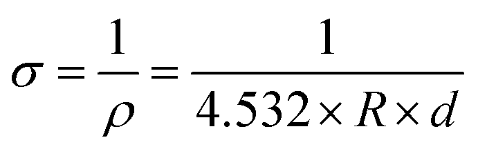 , where ρ is the resistivity of the material. R and d are the resistance and thickness of the prepared pellet.12,18,28 The high and low current ranges during the measurement were recorded in the range from 20 × 10−6 to −20 × 10−6 A, and the delta voltage step was fixed at 100 mV s−1 for all the samples. The electrochemical properties were recorded with a PARSTAT 4000 (Princeton Applied Research, USA) electrochemical workstation using 1 M Na2SO4 as the electrolyte. Specific capacitance was calculated from the CV curves using the equation: CCV = (∫IdV)/mυ, where CCV is the specific capacitance (F g−1), I is the response current density (A g−2), V is the potential window, υ is the scan rate (mV s−1), and m is the deposited mass on the electrode.12,29–31 The specific capacitance can be calculated in terms of the discharge time according to the equation: CCD = IΔt/mV, where CCD is the specific capacitance (F g−1), I is the discharging current (A g−1), V is the potential window (V) and m is the deposited mass on the electrode.12,30,31 The mass balance of the electrodes for asymmetric configuration was done according to the relation:
 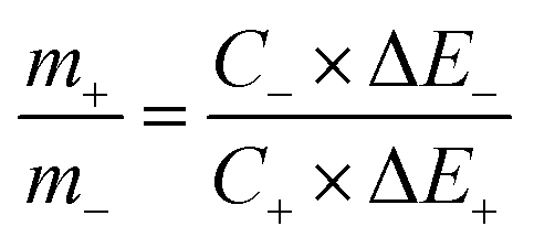 , where m+ and m− are the mass of the positive and negative electrodes, C+ and ΔE+ are the specific capacitance and potential window (calculated from the three electrode measurement) for the positive electrode, and C− and ΔE− are the specific capacitance and potential window of the negative electrode measured at the same scan rate.12,32,33 The energy density (ED) and power density (PD) can be calculated according to the formula, ED = CV2/2 and PD = ED/ΔT, where C is the specific capacitance, V is the operating voltage, and ΔT is the discharge time.12,33,34