Printed flexible thermoelectric materials and devices
Jiaqing
Zang†
a,
Jiayi
Chen†
b,
Zhewei
Chen
a,
Ya
Li
a,
Jiye
Zhang
 *b,
Tao
Song
 *a and
Baoquan
Sun
 ac
ac
aJiangsu Key Laboratory for Carbon-Based Functional Materials & Devices, Institute of Functional Nano & Soft Materials (FUNSOM), Soochow University, Suzhou 215123, P. R. China. E-mail: tsong@suda.edu.cn
bSchool of Materials Science and Engineering, Shanghai University, Shanghai 200444, P. R. China. E-mail: jychang@shu.edu.cn
cMacao Institute of Materials Science and Engineering, Macau University of Science and Technology, Taipa 999078, Macau SAR, P. R. China
First published on 30th June 2021
Abstract
The innate capability of direct heat–electricity conversion endows thermoelectric (TE) materials with great application potential in the fields of low-grade heat harvesting, solid-state cooling, and sensing. Recently, the rapid development of information technology such as the Internet of Things and the popularization of wearable electronic devices have stimulated a period of prosperity for the research on flexible thermoelectric (FTE) devices. At the same time, the research on printed electronics (PEs) is expected to provide scalable and cost-effective manufacturing approaches for FTE devices. This review focuses on the recent progress in printed flexible thermoelectric (PFTE) devices and their applications. At first, the fundamental theories behind TEs and the related performance optimization strategies for FTE devices, as well as the history and applications of PEs, are introduced. Then, the state-of-the-art materials adopted in FTE devices, including materials for TE legs, solvents, dispersants, surfactants, and adhesives for printable inks/pastes, substrates, and electrodes, and the related printing methods are summarized. Subsequently, the applications and device performance of PFTE devices in thermoelectric generators (TEGs), thermoelectric coolers (TECs) and thermoelectric sensors (TESs) over the last decade are reviewed. At last, the challenges existing currently in the PFTE field are discussed and some perspectives on the future investigations toward high-performance, low-cost PFTE devices are proposed.
1. Introduction
The capability of directly interconverting heat and electricity endows thermoelectric (TE) materials with potential for application in the fields of power generation, refrigeration and sensing.1–3 Therefore, TE conversion technology has been considered to be a feasible solution to both the serious energy crisis and environmental issues.4 For example, TE devices can harvest the ubiquitously dispersed and low-grade heat energies emanating from the sun, industrial equipment, automobiles, or even the human body, and convert the heat into electricity.5 Accordingly, electrical power can in turn drive TE devices as heat engines for solid-state cooling or active temperature control.6 Nevertheless, compared with other energy conversion strategies, such as photovoltaic power generation and vapor compression refrigeration, TE conversion has much lower efficiency. Thus, the applications of TE devices have long been limited to niche scenarios, such as space missions, laboratory equipment, and medical applications.7 Fortunately, benefiting from the development of integrated circuits in the last decade, the power consumption of microelectronic systems has continued to decrease, which stimulated an unprecedented boom in smart wearable and implantable electronic devices. Furthermore, the recent popularity of 5G technology and the Internet of Things (IoTs) is driving wearable and implantable electronic devices towards miniaturization, integration and low power consumption. Therefore, optimizing the device energy supply mode and simplifying the device configuration have become key issues that need to be urgently resolved in this field, which may expand hugely the application and market space for TE materials. Based on their characteristics of solid state, fast response, long life, no moving parts and easy miniaturization, TE devices will play important and versatile roles in wearable and implantable systems, such as self-power supplies, active temperature management, and environmental/body monitoring. Among them, flexible thermoelectric (FTE) modules should be more promising candidates for wearable electronics because of the merits of light weight and good comfort. In addition, their deformability can also enable better thermal contact with heat sources of arbitrary shapes, which is specifically important in either heat harvesting or component cooling applications.Recently, the vigorous development of printed electronics (PE) has provided a large-scale and low-cost fabrication method for FTE devices. PE refers to a typical kind of electronics manufactured by various printing technologies (e.g., inkjet printing,8–11 nanoimprinting lithography,12–14 aerosol jet printing,15,16 screen printing17–19), which have evolved from laboratory to fabrication (lab to fab) in the past few decades.20–22 Although these technologies are not comparable to silicon-based microfabrication technologies (e.g., vacuum thermal evaporation, chemical vapor deposition, magnetron sputtering) when it comes to high integration, resolution and information capacity, PE has received considerable attention due to its superiority in flexibility, cost effectiveness, and large-area production. What's more, printed TE devices make the fabrication process simple, effective and low cost, which will make a difference in commercial application.
This review is aimed to provide a snapshot of the recent progress in printed flexible thermoelectric (PFTE) devices and their applications. We start by introducing the fundamental theory of TEs and the related performance optimization methods for PFTE devices, as well as the history and applications of PEs. Then, materials and printing methods adopted in FTEs are summarized. Finally, the applications and device performance of FTEs in thermoelectric generators (TEGs), thermoelectric coolers (TECs) and thermoelectric sensors (TESs) over the last decade are reviewed.
2. Fundamentals of TEs
The complete theoretical system describing the direct TE energy conversion was established by Thomas Seebeck, Jean Peltier and William Thomson between 1821 and 1857.23 The TE effect (Seebeck effect) was first discovered by Thomas Seebeck in 1821, which showed that an electromotive force could be produced by heating the junction between two different conductors and quantified using the Seebeck coefficient, S = V/ΔT, in which ΔT is the temperature difference established between the two conductors and V is the open-circuit electromotive force induced by ΔT. Thirteen years later, Peltier discovered the inverse counterpart of the Seebeck effect, namely the Peltier effect, who observed heating or cooling at the junction of two different conductors when electric current passes through the circuit. The phenomenon originated from the variation in the average energy of carriers between different materials and can be measured using the amount of energy (q) transported per unit carrier, i.e., the Peltier coefficient, π = q/I, where I is the current passing through the circuit. Apparently, the Peltier and Seebeck effects should be closely related. However, their interdependency was not fully established until William Thomson (who later became Lord Kelvin) proposed the Kelvin relation based on the theory of thermodynamics about thirty years later,24 who also predicted a third TE effect, the Thomson effect. The Kelvin relation can be expressed as π = ST (T, the temperature), which provides us with great convenience for evaluating and characterizing the TE conversion performance of materials, because it is much simpler to measure the Seebeck coefficient than the Peltier coefficient.Practical TE conversion devices usually make use of modules that contain a number of unicouples composed of both p- and n-type materials connected electrically in series and thermally in parallel (Fig. 1). The Seebeck coefficients of n-type materials (Sn) are negative, whereas those of p-type materials (Sp) are positive. The performance of a TE device working in power generation mode and cooling mode can be evaluated using the energy balance equations at the hot side and cool side, respectively, and can be represented as follows:25
| Qh = (Sp − Sn)ThI − 0.5I2R + K(Th − Tc) | (1) |
| Qc = (Sp − Sn)TcI − 0.5I2R − K(Th − Tc) | (2) |
 | (3) |
 | (4) |
 | (5) |
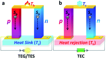 | ||
| Fig. 1 Schematic illustration of the physical processes of TE unicouples used for (a) TEGs/TESs and (b) TECs. | ||
Thus, the maximum output power (Pmax) can be achieved when R = Rl, which is expressed by eqn (5). When a TE unicouple is working in cooling mode, the temperature difference ΔT = Th − Tc can be derived from eqn (2):25
 | (6) |
The maximum temperature difference (ΔTmax) under the optimum operating current between the cold and hot sides can be obtained at zero heat load (Qc = 0) as expressed by eqn (7):25
 | (7) |
 | (8) |
According to the above theoretical analysis, the performance of a TE module is related to the quantity of ZM = Snp2/RK. If the contact electric resistance and thermal resistance in the working circuit are ignored, ZM could be calculated from the properties of TE materials. Accordingly, in the TE community, a dimensionless TE figure of merit, ZT = TS2σ/κ, is introduced to evaluate the performance of a single component TE material, where σ and κ are the electrical and thermal conductivity, respectively. Therefore, a desirable TE material should have high S, high σ, but low κ to achieve a high ZT. At present, reducing the κ of materials, particularly the lattice thermal conductivity (κL), is an effective way to improve ZT, including nanostructuring,26,27 alloying,28 constructing all-scale hierarchical architectures29,30 and seeking materials with intrinsically low κ.31,32 Besides κ, from eqn (5) and (8), it can be deduced that the Pmax and Qc,max of TE devices are proportional to S2σ, which is also known as the power factor (PF) in the TE field. Particularly for the application of FTE devices, we believe that the current top priority is to improve the Pmax of power generation devices and the Qc,max of cooling devices. Therefore, this review mainly focuses on readily effective approaches for improving the PF of FTE materials.
Optimizing carrier concentration (n) is a fundamental approach to improve the PF of TE materials and is also an optimization method often adopted in FTE devices.33,34 The relationships of n, S and σ can be described as:35
 | (9) |
| σ = neμ | (10) |
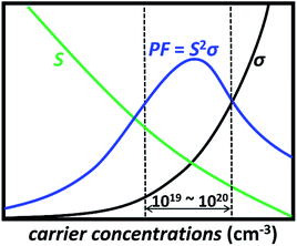 | ||
| Fig. 2 Qualitative dependences of Seebeck coefficients (S), electrical conductivities (σ) and power factor (PF) vs. carrier concentrations. | ||
Carrier mobility is an important parameter for most electronic devices. Particularly for TE devices, carriers are the ‘real’ working substance. Therefore, increasing the μ of a material is also an important method to improve the TE performance. For FTE devices, the subsequent heat treatment is one of the effective methods to improve μ by increasing the crystallinity of the material and reducing the grain boundary.37,38 In addition, there are many other factors closely correlated with PF, such as band convergence,39 resonant levels,40 energy-filtering effect,41etc. However, these methods for PF improvement have yet to be applied in printing FTE devices.
3. History of PE and its applications
Organic electronics originated in 1986 when the first organic field effect transistor (OFET) was reported.42 Simultaneously, an organic light emitting diode (OLED) was produced by Tang et al. for the first time in 1987.43 After that, more and more efforts have been devoted to this area. Researchers started to combine the advantages of printing technologies with organic electronics to realize flexible and stretchable electronics. However, it was not until 1997 when a printed field-effect transistor (FET) was reported for the first time, in which all the essential functional layers were screen-printed on an ITO-coated plastic substrate.44 Since then, printed electronics on flexible support substrates (e.g., polyimide (PI), polydimethylsiloxane (PDMS), polyethylene naphthalate (PEN), poly(ethylene terephthalate) (PET), paper, and glass fabric) progressed at an unprecedented pace for thin film transistors (TFTs),42,45,46 light emitting diodes (LEDs),47 solar cells,48,49etc.3.1 TFTs
TFTs mainly consist of three components: source, drain, and gate electrodes. The semiconductor channel is typically located in the middle of source/drain electrodes while the gate dielectric is placed between the gate electrode and the semiconductor channel.21 Generally, TFT devices applied in conformable active-matrix displays, wearable or textile-integrated devices are facing technical challenges, such as large-area uniformity, device degradation, and dedicated fabrication processes. New forms of flexible or printable TFTs compatible with displays, sensors and memory devices are urgently needed. With the fast development of printing technologies, the performance of flexible TFTs is greatly enhanced. For example, in 2009, Yan et al. described all-printed polymeric complementary inverters, and the electron mobilities of the as-fabricated transistors can reach 0.1 cm2 V−1 s−1 with an on/off ratio of 106 under ambient conditions (Fig. 3a).50 Later on, Jung et al. demonstrated all-printed TFTs and radio frequency identification (RFID) tags via inkjet and pad printers. Besides, they also demonstrated roll-to-roll (R2R) printed RFID tags with printed ring oscillators and rectifiers under a high speed. The unit price is as low as 0.03 dollars per unit, paving the way toward large-scale fabrication based on traditional printing methods.51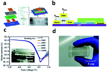 | ||
| Fig. 3 (a) Organic thin-film transistor structure; reproduced from ref. 50 with permission from Springer Nature. (b) Schematic illustration of thin-film transistors produced via roll-to-roll gravure-printing; reproduced from ref. 47 with permission from American Chemical Society. (c and d) Fully screen-printed (AMECD) device and the device performance. Reproduced from ref. 46 with permission from the Royal Society of Chemistry. | ||
Furthermore, Cao et al. developed an active-matrix electrochromic display (AMECD) device with carbon nanotube TFTs.47 Single-walled carbon nanotubes (SWCNTs) have attracted enormous attention owing to their flexibility, solution processability, and compatibility with various printing methods. A screen-printed transistor yields high device output with good mobility (up to 3.92 ± 1.08 cm2 V−1 s−1) and high on/off ratios (∼104) (Fig. 3b). In addition, this TFT has also been integrated into an AMECD, demonstrating the applicability of printed SWCNTs in flexible TFTs. Similarly, Ren et al. constructed their TFT via aerosol jet printing. The SWCNTs show outstanding performance (on/off ratios over 106, good mobility of 9.8 cm2 V−1 s−1 and low hysteresis). Moreover, the as-fabricated TFTs have been used for ammonia (NH3) sensors with higher sensitivity than polymer-sorted devices (Fig. 3c and d). In the end, both the fully-printed TFTs and NH3 gas sensors exhibit excellent conformity and stability.46
3.2 OLEDs
After four decades of development since Tang's finding in 1987,43 OLEDs have become some of the mainstream display technologies due to their unique advantages, such as fast response time, wide viewing angle, excellent contrast ratio, high dynamic range, etc. Besides, the organic nature of functional materials in OLEDs is compatible with the applications of flexible and wearable devices (VR/AR headsets and smart wristbands). In 1998, Hebner et al. developed a patterned luminescent doped polymer via inkjet printing and successfully applied it for OLED application, which is the initial attempt to develop flexible OLEDs.52 After that, Kopola et al. put forward a large-area polymer-based OLED device via the gravure printing technique (Fig. 4a). This LED shows a brightness of 100 cd m−2 under a bias of 4.2 V. This work displays the outstanding properties of the printing technology in terms of low cost, high yield and mass production.53 Besides, Juan Zhu et al. demonstrated blade-coated OLEDs on transparent metal micromesh (TMM) electrodes.54 The printed OLEDs present a low turn-on voltage of 3.4 V and the peak brightness could reach 4000 cd m−2 at 6.5 V as shown in Fig. 4b and c. Finally, an external quantum efficiency (EQE) of 3.6%, and a luminous efficiency of 1.4 lm W−1 was achieved.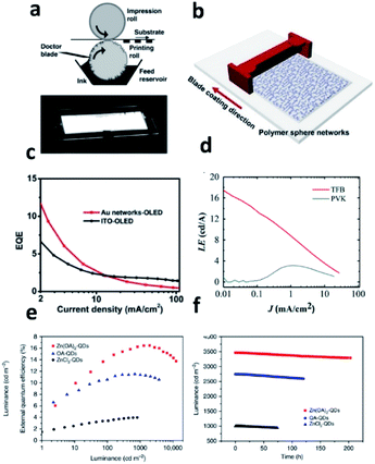 | ||
| Fig. 4 (a) Schematic of large-scale OLED production via gravure printing; reproduced from ref. 53 with permission from Elsevier. (b) Fabrication process of Au micromesh transparent electrodes via blade-coating. (c) Device performance (EQE–J) of printed OLEDs; reproduced from ref. 54 with permission from American Chemical Society. (d) Inkjet-printed OLEDs (LE–J); reproduced from ref. 55 with permission from the Royal Society of Chemistry. (e and f) EQE and life time of Zn(OA)2-QDs vs. OA-QDs vs. ZnCl2-QDs devices; reproduced from ref. 56 with permission from Springer Nature. | ||
Mu et al. fabricated their emitting layer with a single solvent. Their newly developed host was compatible with inkjet printing. And the single solvent strategy simplified the production process. Eventually, the OLED showed a high current efficiency of 17.89 cd A−1.55 With the same printing technology, Xiang et al. presented a dual ionic passivation strategy for inkjet-printed quantum dot light emitting diodes (QLEDs). The trap states could be reduced efficiently with the passivation of Zn(OA)2 organic salt (Fig. 4e). Therefore, the device showed high stability for over 1![[thin space (1/6-em)]](https://www.rsc.org/images/entities/char_2009.gif) 721
721![[thin space (1/6-em)]](https://www.rsc.org/images/entities/char_2009.gif) 000 hours (Fig. 4f), which paved a way for mass production of QLEDs.56
000 hours (Fig. 4f), which paved a way for mass production of QLEDs.56
3.3 Solar cells
In the 20th century, Matsumoto et al. produced a CdS/CdTe solar cell via a screen-printing process. The maximum power conversion efficiency (PCE) was 12.8% with an active area of 0.78 cm2.57 In 2010, Frederik C. Krebs reviewed the development of polymer solar cells from lab-to-fab. They focused on the price and instrument requirements. Besides, their work emphasizes that the printing technology may pave the way for mass production of flexible solar cells.58 In addition, Chen et al. produced their single crystalline silicon solar cells based on Al nanoparticles, which ought to enhance the device performance (Fig. 5a).59 Their work provided a simple and low-cost way to produce textured solar cells. In addition, photovoltaic devices based on these tools have also become a hot topic since the emergence of metal halide perovskite solar cells (PSCs). FAPbI3-based perovskite layers were reported by Young Yun Kim et al. The best PCE of gravure-printed flexible PSCs can reach 19.1%, which is one of the highest PCEs in flexible PSCs (Fig. 5b and d).48 Fabian Schackmar et al. introduced a fully inkjet printing process for PSCs.49 The as-fabricated PSC exhibits a peak PCE of 17% and excellent stability in the ambient atmosphere as shown in Fig. 5e.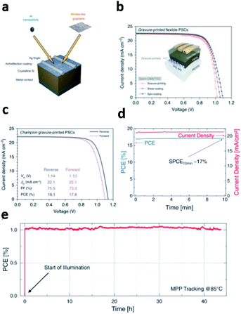 | ||
| Fig. 5 (a) Schematic of the proposed Al nanoparticles/graphene-enhanced single crystalline silicon solar cells; reproduced from ref. 59 with permission from Springer Nature. (b) J–V curve of PSCs, reproduced from ref. 48 with permission from John Springer Nature; (c) J–V curves of perovskite solar cells produced via gravure printing; reproduced from ref. 49 with permission from John Wiley and Sons. (d) Maximum power point (MPP) tracking at 25 °C, reproduced from ref. 48 with permission from John Springer Nature; (e) MPP tracking at 85 °C under illumination with high stability. Reproduced from ref. 49 with permission from John Wiley and Sons. | ||
3.4 Other PE devices
Apart from the devices above, printing technologies have also been utilized in other areas. For instance, Glushkova et al. demonstrated 3D aerosol jet printed X-ray detector units with a record device performance, which is up to 2.2 × 10⁸ μC Gyair−1 cm−2, a giant step toward high sensitivity devices.60 Moreover, due to a possible self-healing mechanism, MAPbX3-based devices have recently been shown to exhibit exceptional reliability under radiation. Furthermore, Zhu et al. used 3D printing technology in flexible triboelectric nanogenerator (TENG) devices.61 The Voc, Isc, and power density of 610 V, 1.9 mA, and 6.1 W m−2 were obtained. The authors think that the integration tools may further push the advancement of new materials for commercial use. Overall, PEs are promising for the mass production of portable flexible devices for numerous applications in the future.The advances of different types of printing techniques provide a new era of electronic units for realizing commercial application and large-area production. The revolution of this era is like a raging fire, which has influenced TE devices.19 Inspired by the development history, we envisage that flexibility will dominate the next-generation TE devices.
4. Materials for PFTE devices
4.1 Materials for TE legs in flexible modules
In order to realize high-performance FTE devices, it is very important to explore flexible TE materials suitable for various printing methods. At present, there are mainly three strategies to realize flexibility of TE materials. The first is the use of extensively used nanostructured rigid inorganic materials, such as Bi2Te3, Sb2Te3 or their alloys, which can achieve flexibility to some extent when deposited on flexible substrates. The second is the use of two dimensional (2D) inorganic TE materials (such as graphene and TiS2), which can be effectively peeled off and dispersed in a solvent to form FTE films.62,63 The third method is to use inherently flexible organic TE materials, such as poly(3,4-ethylenedioxythiophene) (PEDOT):poly(styrenesulfonate) (PSS), polyaniline (PANI), etc. Although such materials possess intrinsic low electrical transport properties (both in σ and S), their performance can still be improved through enhancing the crystallinity or suitable post-treatments (see the detailed discussion in Section 4.1.2). In addition, during the preparation of FTE devices, the solvents, dispersants, and adhesives used in ink preparation have an important influence on the viscosity, density, surface tension and the subsequent curing characteristics of the ink. The substrate materials and electrode materials are also key aspects to modulate the flexibility, heat treatment temperature, and interface electric and thermal resistance of FTE devices. Therefore, in this section, we introduce and discuss materials for TE legs in flexible modules, substrates, and electrodes.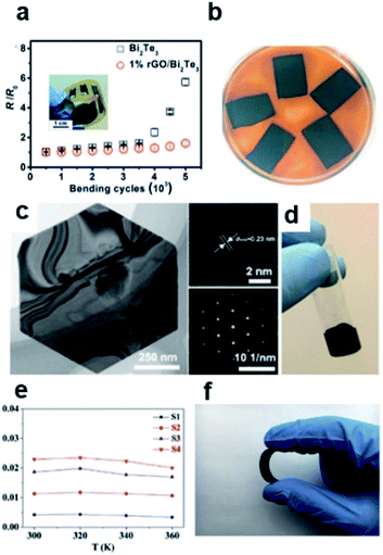 | ||
| Fig. 6 (a) R/R0 of a 1% rGO/Bi2Te3 device with a bending radius of 5 mm (R and R0 are the resistances before and after bending, respectively). The R value of the 1% rGO/Bi2Te3 device after 1000 bendings is 1/5 of the R value of the Bi2Te3 device. rGO/Bi2Te3 devices show excellent flexibility. Reproduced from ref. 64 with permission from the Royal Society of Chemistry. (b) GO film reduced by copper. Reproduced from ref. 65 with permission from Elsevier. (c) TEM and HRTEM of Bi2Te2.7Se0.3 nanoplates. Reproduced from ref. 66 with permission from John Wiley and Sons. (d) Physical image of synthetic ink. (e) The ZT values of different CB/BTBA/PLA samples vary with temperature. (f) Flexibility of CB/BTBA/PLA composite materials. Reproduced from ref. 69 with permission from Elsevier. | ||
Zeng et al. used a scalable, low-temperature, and solution-processable method to manufacture large-area continuous conductive rGO nanosheets, employing PET and 3D printed PDMS grids as substrates (Fig. 6b).65 The electrical conductivity and thermal conductivity of the nanosheets are affected by the longitudinal carrier mobility of the lattice domain and the phonon scattering caused by defects. Due to the high carrier mobility and strong phonon scattering, the electrical conductivity of the film is enhanced. The thermal conductivity decreases, and the electrical conductivity at room temperature (RT) is 1.43 × 10⁴ S m−1. The rGO film is assembled on a 3D printed PDMS grid to prepare a flexible TEG. When ΔT = 50 K, its output voltage per unit mass is 57.33 mV g−1. The wristband-type flexible TEG has 7 repeating units and can generate a maximum power density of 4.19 μW g−1 at an ambient temperature of 15 °C, which shows the potential application prospects of wearable TEGs.
Zhang et al. prepared Bi2Te2.7Se0.3 nanoplate ink (Fig. 6c and d). After solution treatment, it was printed on paper, polyimide and glass tubes using 3D conformal aerosol jet printing technology and a fast photon sintering process.66 Bi2Te2.7Se0.3 nanoplates were synthesized by a simple solution route. Bi(NO3)3, Na2TeO3 and SeO2 were dissolved in EG. Then, NaOH and PVP were sequentially added with vigorous stirring, and the mixed solution was refluxed at a temperature of 185 °C under a nitrogen atmosphere. After the mixture was cooled to RT, the prepared Bi2Te2.7Se0.3 nanoplates were precipitated with acetone, and then redissolved in ethanol. This process is repeated until unreacted chemicals and EG are removed from the surface. Finally, the printing ink is obtained by mixing the prepared Bi2Te2.7Se0.3 nanoplates, EG, glycerin and ethanol. Within a few seconds of photonic sintering, the conductivity of the printed Bi2Te2.7Se0.3 film was significantly increased from non-conductivity to 2.7 × 10⁴ S m−1. The RT power factor of these films is 730 μW m−1 K−2, which may provide opportunities to transform semiconductor nanocrystals into functional and flexible devices suitable for various industrial and wearable applications.
Zhao et al. prepared a flexible Bi0.5Sb1.5Te3/epoxy composite TE film on a polyimide substrate by screen printing.67,68 The active component for the printable inks/slurries was ball-milled Bi0.5Sb1.5Te3 powder from ingots synthesized by a conventional melting method. The electrical transport properties of the film are affected by the content of the Bi0.5Sb1.5Te3 powder. The Pmax of the optimized Bi0.5Sb1.5Te3/epoxy resin film is 1.12 μW m−1 K−2 (T = 300 K). This composite film can withstand a bending strength of more than 20 mm. The flexible TE arm of the prepared TE device can establish a temperature difference of 4.2 °C to 7.8 °C under an operating current of 0.01 A to 0.05 A, showing potential applications in the field of planar cooling.
Du et al. have constructed flexible ternary carbon black/Bi2Te3-based alloy/polylactic acid (CB/BTBA/PLA) composite materials based on commercially available Bi0.4Sb1.6Te3 powder (200 mesh) through additive manufacturing (3D printing) technology.69 As the mass ratios of BTBAs reached 71.4%, the power factor of the composites is about 19.2 μW m−1 K−2 at 300 K (Fig. 6c and d).
Chen et al. ink-jet printed Bi2Te3 and Bi0.5Sb1.5Te3 nanowires (NWs) synthesized by a low-temperature solution-phase strategy on polyimide to form TE unicouples, and then connected them with eutectic gallium–indium (EGaIn) liquid metal in series.9,70 The printing ink is simply obtained by dispersing nanowires in deionized (DI) water by bath sonication. It is found that the maximum power factors of Bi2Te3 and Bi0.5Sb1.5Te3 nanowires are 180 μW m−1 K−2 and 110 μW m−1 K−2, respectively. At a temperature difference of 32.5 K, the Pmax of a fully printed TEG device is up to 127 nW. Furthermore, even after multiple bending experiments (up to 50 times) around the tight radius of curvature (rod diameter 11 mm), the performance of the TEG device was not decreased.
Carbon nanotubes are also promising candidates for PFTE devices. Liu et al. reported boron-doped single-walled carbon nanotubes (B-SWCNTs) with improved S and σ, resulting in a PF value of 226 μW m−1 K−2.71 Inspired by this result, using B-SWCNT dispersion and silver paste as materials, a printable TEG with a length of 253 mm was designed and manufactured on PI (Kapton) strips. The generator is composed of 61 single p-legs. When ΔT is 60 K, the maximum output voltage and power output reach 20 mV and 400 nW, respectively.
The TE performance of PEDOT:PSS can also be substantially improved by various post-treatment procedures, including doping/dedoping,41 acid/alkali treatment,77 tuning the oxidation levels and annealing.73,78 Yi et al.79 introduced binary secondary dopants, dimethyl sulfoxide (DMSO) and poly(ethylene oxide) (PEO) into PEDOT:PSS, and found that addition of 5% DMSO and 0.3% PEO could simultaneously increase its σ and S to ∼1061 S cm−1 and ∼38.4 μV K−1, respectively. Chen's group73 adopted sequential triple post-treatments with formamide (CH3NO), concentrated sulfuric acid (H2SO4), and sodium borohydride (NaBH4) to optimize the TE properties of PEDOT:PSS films. It is found that treatment with CH3NO and H2SO4 effectively removed excess PSS, increased the crystallinity and thus the carrier mobility of the sample. The final post-treatment with NaBH4 solution increased both the σ and S of the PEDOT:PSS sample by tuning its oxidation level. It is also reported by Huang et al.78 that extraordinary power factor could also be obtained for PEDOT:PSS films via improved molecular crystallinity by annealing and subsequent organic solvent post-treatment. The recent breakthroughs in PEDOT-based materials facilitate their application in PFTE devices.
Kee et al. demonstrated a TE material with high deformability and excellent rapid self-healing ability prepared by 3D printing technology (Fig. 7d).80 The material is based on PEDOT:PSS and polymer surfactants, and Triton X-100 is used as a curing agent. It is mixed with dimethyl sulfoxide (DMSO) additive as a ternary composite material of TE performance enhancer. Upon repeatedly cutting this composite film or completely cutting the composite film on the PDMS substrate into two parts, the current level and mechanical level of the composite film can quickly recover to the original level. In this composite material, the liquid surfactant can act as a soft matrix area, and the active matrix entangled with PEDOT:PSS flows from both sides to the void area, thus forming physical contact. In addition, the polyethylene oxide-based hydrogen bonding site of Triton X-100 can help the cut composite film to recombine at the cutting interface, which successfully restores the electrical connection and TE properties of the composite film. When the surfactant content increases, the Seebeck coefficient of the composite membrane remains basically unchanged, and the electrical conductivity decreases significantly, but its self-repairing ability becomes stronger. In this ternary composite material, DMSO enhances the electrical conductivity, which doubles the PF of the material. In addition, because the surfactant induces the amorphous phase, the in-plane thermal conductivity of the composite film is as low as 0.27 W m−1 K−1. A 3D printed TE generator fabricated using this ternary composite material can produce a Pmax of 12.2 nW on a 328 Ω load resistance (Fig. 7e).
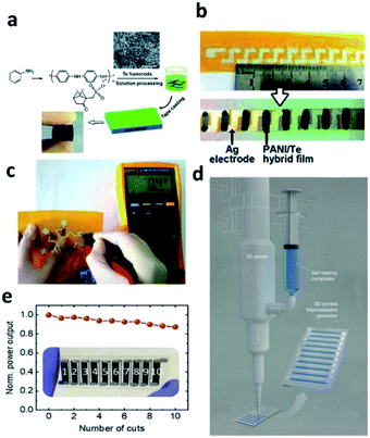 | ||
| Fig. 7 (a) PANI/Te hybrid membrane preparation flow chart, in which the embedded picture is a 60 wt% Te hybrid membrane. (b) Manufacturing PANI/Te single-leg equipment. (c) A single leg is touched with fingertips, and the micro-TE conversion function is displayed. Reproduced from ref. 81 with permission from the Royal Society of Chemistry. (d) 3D printer equipment and printing process. (e) The relationship between normalized power output and cutting times. The embedded picture is a 3D printed TEG module. Reproduced from ref. 80 with permission from John Wiley and Sons. | ||
Huang et al. fabricated flexible TE modules using PEDOT:PSS coated paper and indium tin oxide (ITO) conductive film as p-type TE legs and n-type TE legs, respectively.82 PEDOT:PSS forms a continuous conductive layer by filling the gaps between cellulose fibers. Compared with the bare paper, PEDOT:PSS paper has lower resistance and good conductivity, which shows that PEDOT:PSS can be successfully assembled on the surface of commercial office paper. Then, they designed an integrated detection device using 3D printing technology that can be used for the detection of biomolecules.
Generally, PEDOT:PSS is a p-type doped conductive polymer, but in order to realize conventional TE unicouples, an n-type conductive polymer is also needed. Yang et al. prepared ethanol-based poly(benzimidazole-benzophenanthroline):poly(ethyleneimine) (BBL:PEI) printable n-type conductive ink.83 The electrical conductivity of this n-type TE film reached 8 S cm−1, and its thermal stability, environmental stability, and solvent stability are excellent. They printed BBL:PEI (33 wt%) n-type TE legs and PEDOT:PSS p-type TE legs to prepare flexible all-polymer TEGs. When ΔT = 50 K, each pair of p–n TE legs has a high power output of 56 nW, which is hitherto the highest reported value of in-plane all-polymer TEGs.
Jang et al. used 2,3,5,6-tetrafluoro-7,7,8,8-tetracyano-quinodimethane (F4TCNQ) as a dopant to enhance the electrical conductivity and Seebeck coefficient of the poly(3-hexylthiophene) (P3HT) polymer.84 Because of the high electron affinity of F4TCNQ, it can be used as an electron acceptor for p-type doping of polymers. In the ambient air atmosphere at RT, the electrical conductivity of the P3HT polymer increased by about 6 to 7 orders of magnitude, after being doped with 17 wt% F4TCNQ (2.62 S cm−1). The relevant S is about 109 μV K−1, yielding a PF value up to 2.44 μW m−1 K−2, which is an order of magnitude higher than those of previous reports. However, an excessive amount of F4TCNQ leads to the formation of impurities and phase separation, and thus decreases the electrical conductivity of the samples.
In hybrid TE materials, the inorganic additives mainly include carbon nanotubes, graphene nanosheets and other inorganic nanostructures.85 Wang et al. designed a conductive polymer with a matching interface and an inorganic semiconductor nanocomposite (PANI/Te nanorod hybrid composite system) with high Seebeck coefficient (Fig. 7a).81 Te nanocrystals promote the extension of the polymer chain and help improve the conductivity of the composite film. In addition, the interface of Te and conductive polymer PANI was tightly combined, and the in situ polymerization reaction between them made the nanofillers uniformly dispersed. When the Te content is 70 wt%, the conductivity reaches the maximum value of 102.5 S cm−1. The maximum value of ZT at 383 K was 0.23. Compared with the PEDOT:PSS/Te film, the conductivity of the PANI/Te film is an order of magnitude higher. Then, they designed a single-leg TE conversion device based on this hybrid composite (Fig. 7b), and it can be seen from Fig. 7c that the device exhibits moderate TE conversion performance.
C. Meng et al.86 reported that PANI/carbon nanotube (CNT) composites would exhibit higher S and PF than PANI alone. Due to the energy filtering effect, the S and maximum PF of the PANI/CNT composite at 300 K reach 28.6 μV K−1 and 5.0433 μW m−1 K−2, respectively. After that, Yao et al.87 proposed PANI/single-walled carbon nanotube (SWCNT) composites with enhanced PF prepared by in situ polymerization, in which a PANI layer tightly wrapped the surface of SWCNTs. The strong π–π interaction between PANI and SWCNTs led to more ordered chain structures of PANI and thus increases in both σ and S. As a result, the maximum PF of their PANI/SWCNT system reached 20 μW m−1 K−2.
Kim's team has conducted continuous research on PEDOT:PSS/Ag2Se nanowire (NW) composites.88,89 At first, the PF of the prepared film could reach 178.59 μW m−1 K−2. Subsequently, by using an in situ solution-phase synthesis method, they further improved the PF of the PEDOT:PSS/Ag2Se NW film to 327.15 μW m−1 K−2. Under a temperature difference of 20 K, the output voltage of the TEG device consisting of five composite legs was up to 7.6 mV. Lee et al.90 found that adding zinc oxide (ZnO) particles into the aqueous solution of PEDOT:PSS could effectively increase its viscosity, which facilitated the preparation of thick free-standing composite sheets needed for vertically stacked TE devices. In addition, the introduction of ZnO additives could also improve the σ of the PEDOT:PSS.
Zhang et al.91 reported a PPy/rGO composite with a 3D interconnected architecture constructed by a new interfacial adsorption-soft template polymerization strategy. The TE properties of the composite nanomaterials are significantly improved compared with those of pure PPy nanowires. At room temperature, the maximum PF of the composite reaches 8.56 μW m−1 K−2, which is about three times larger than that of the previously reported PPy/rGO composite films.92
In addition, ternary composite TE materials have also been extensively studied. Choi et al.93 prepared a graphene/polymer/inorganic nanocrystal (PEDOT:PSS/rGO/Te nanowire) ternary composite TE material. This ternary hybrid system consisted of two heterojunctions, i.e. PSS/rGO and PEDOT:PSS/Te nanowires, which could induce double-carrier filtering and significantly increase σ while maintaining the S. At 300 K, the PF of the ternary hybrid is 143 μW m−1 K−2, which is much higher than those of the binary systems. Cai et al.94 fabricated a PEDOT/Ag2Se/CuAgSe composite film on a nylon membrane. Due to the synergistic effect of the PEDOT and Ag2Se/CuAgSe phase and the carrier-filtering effect at the multi-heterointerfaces, the composite film simultaneously shows an ultrahigh PF of about 1603 μW m−1 K−2 and a low κ at 300 K.
In the process of drop-on-demand inkjet printing, the behaviour of ink drops can be described by several dimensionless physical constants, the most useful being the Reynolds (Re) number, Weber number (We), and Ohnesorge number (Oh):
 | (11) |
 | (12) |
 | (13) |
In addition, the factors limiting the generation of droplets are affected by the surface tension of the liquid–air interface at the nozzle, which must be overcome before the droplets can be ejected. Duineveld et al. presented the minimum velocity at which the droplets can be ejected from the nozzle:97,98
 | (14) |
The maximum allowable velocity of the droplet in collision with the substrate was first raised by Stow and Hadfield.
 | (15) |
In inorganic material ink, Bi2Te3-based materials exhibit the best TE properties at RT, and the effects of their composition and microstructure on the TE properties have been widely studied. Typically, depending on the type of printhead, an ink with surface tension of 20–40 mN m−1 and viscosity of 5–20 cP is suitable for inkjet printing. The results show that the surface tension and viscosity of aqueous TE dispersion cannot meet the printing requirements. Lu et al. improved the dispersity by adding a less volatile solvent, dipropylene glycol monomethyl ether (DPM), which has lower surface tension and higher viscosity than water. Its chemical structure is shown in Fig. 8a. At a mass ratio of 1![[thin space (1/6-em)]](https://www.rsc.org/images/entities/char_2009.gif) :
:![[thin space (1/6-em)]](https://www.rsc.org/images/entities/char_2009.gif) 1 (dispersion: DPM), the surface tension and viscosity of the ink are suitable for printing (32 mN m−1 and 6 cP, respectively). Besides, the addition of polymeric hyper-dispersant Solsperse 46000 can achieve the chemical and colloidal stability of nanoparticles.99
1 (dispersion: DPM), the surface tension and viscosity of the ink are suitable for printing (32 mN m−1 and 6 cP, respectively). Besides, the addition of polymeric hyper-dispersant Solsperse 46000 can achieve the chemical and colloidal stability of nanoparticles.99
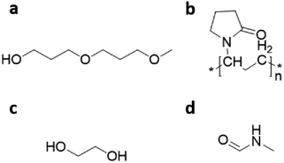 | ||
| Fig. 8 The chemical structure formula of several common additives. (a) Dipropylene glycol monomethyl ether (DPM). (b) Polyvinylpyrrolidone (PVP). (c) Ethylene glycol. (d) N-Methyl formamide. | ||
Among organic–inorganic hybrid inks, graphene-based organic nanocomposites have great potential in the field of TEs. In order to adopt inkjet printing for developing thermostable graphene-based TE devices, the ink of the material needs to be optimized. Researchers prepared graphene dispersions with the assistance of polyvinylpyrrolidone (PVP) from lumpy graphite dispersed in isopropanol (IPA). As a solvent, IPA is widely used in commercial functional inks and pigment-based inks due to its low boiling point, rapid drying, and low toxicity. When graphene is dispersed in IPA alone, graphene tends to precipitate rapidly, whereas the addition of PVP keeps graphene stable in a homogeneous solution (Fig. 8b).100
Screen printing is the most commonly used method for preparing TE devices and is compatible with a wider range of inks than other printing technologies. Organic, inorganic materials and their mixtures can be used in this method. But at the same time, high viscosity of TE inks is required. The viscosity of the paste and the surface tension of the substrate together determine the distribution mass of the paste through the screen mask. In addition, it is worth noting that organic additives such as adhesives affect the properties of TE materials.
In the application research of wearable TEGs, Wen et al. mixed an inorganic material (Bi2Te2.7Se0.3 or Sb2Te3) with organic paste to obtain a TE material for screen printing. The paste was synthesized from liquid epoxy resin, methylhexahydrophthalic anhydride (MHHPA), and 2-ethyl-4-methyl-1H-imidazole-1-propane nitrile (EMIP).101
In organic TEs, the study of in-plane conductivity and the Seebeck coefficient is of great significance for the characterization of organic TE modules. Therefore, the preparation, optimization and characterization of organic TE components play an important role in guiding material design. Researchers conducted a proof-of-concept study of an organic TE module using the benchmark p-type material PEDOT:PSS. The ink is an aqueous solution of PEDOT:PSS containing 5% ethylene glycol to improve its electrical conductivity (Fig. 8c).102
In terms of organic–inorganic hybrid inks, Rösch et al. used TE inks based on PEDOT nanowires and TiS2:hexylamine-complex materials to print a 2D layout on thin flexible substrates to produce a mechanically stable 3D cuboidal device.103 The printing ink of the p-type TE material was prepared by using the synthesized PEDOT nanowires and glycol as the solvent. Wan et al. also reported a TiS2:hexylamine-complex as an n-type FTE material.104 N-type FTE materials were synthesized by electrochemical intercalation. The hybrid superlattice of alternating inorganic TiS2 is injected into the inorganic layer and then stabilized with organic cations to provide n-type carriers for current and energy transmission. The ink is prepared with N-methyl formamide as the solvent (Fig. 8d) (Table 1).103
| Materials | Additive | Process | Seebeck coefficient (μV K−1) | ZT | Ref. |
|---|---|---|---|---|---|
| Sb1.5Bi0.5Te3/Bi2Te2.7Se0.3 | Ethyl cellulose | Screen printing | 210/−170 | 0.93/0.64 | 105 |
| PEDOT:PSS | Ethylene glycol | Screen printing | 25 | — | 102 |
| C60:TiS2 | N-Methyl-2-pyrrolidone (NMP) + IPA | Roll-to-roll printing | −101 | 0.3 | 106 |
| Bi2Te2.7Se0.3/Sb2Te3 | Epoxy resin + methylhexahydrophthalic anhydride + 2-ethyl-4-methyl-1H-imidazole-1-propane nitrile | Screen printing | — | — | 101 |
| BiSbTe | α-Terpineol + Disperbyk-110 | Screen printing | 204 | 1 | 107 |
| Bi2Se2.8Se0.2 | α-Terpineol + Disperbyk-110 | Screen printing | — | 0.43 | 19 |
| BiSbTe/BiTeSe | Methyl cellulose | Screen printing | 209/−165 | 0.65/0.81 | 38 |
| Bi2Te2.7Se0.3 | Ethylene glycol + glycerol | Aerosol jet printing | −163.4 | — | 66 |
| PEDOT nanowires/TiS2 | Ethylene glycol + hexylamine | Screen printing | 25.6/−96.6 | 0.062/0.22 | 103 |
| PEDOT:PSS:Bi2Te3:Sb2Te3 | Ethylene glycol | Aerosol jet printing | 33.8 | — | 108 |
| Bi0.5Sb1.5Te3 | Epoxy resin | Dispenser printing | 200 | 0.2 | 109 |
| Sb1.5Bi0.5Te3/Bi2Te2.7Se0.3 | Solsperse 46![[thin space (1/6-em)]](https://www.rsc.org/images/entities/char_2009.gif) 000 + dipropylene glycol monomethyl ether 000 + dipropylene glycol monomethyl ether |
Inkjet printing | 177/−139 | — | 99 |
| Sb1.6Bi0.4Te3/Bi2Te2.7Se0.3 | Glycerol | 3D printing | 199/−145 | 0.9/0.6 | 110 |
| Graphene | PVP + IPA | Inkjet printing | 55.4 | — | 100 |
| SWCNTs:PVAc | Poly(oxyethylene)4lauryl | Inkjet printing | 148 | — | 111 |
| (PEDOT)0.03V2O5 | Triton X-100 | Inkjet printing | −350 | 0.001 | 112 |
| Bi0.5Sb1.5Te3/Bi2Te3 | PVP | Inkjet printing | — | 0.04/0.13 | 9 |
| Single-crystalline Bi2Te3 | PVP | Inkjet printing | 140 | — | 8 |
4.2 Substrates for FTE devices
Traditional TE devices such as binary chalcogenides (Bi2Te3, Sb2Te3) are extensively used for wearable TE applications thanks to their outstanding ZT values near RT.113–115 However, the flexibility and deformability of these materials are still poor due to their intrinsic rigidness. Therefore, printing technologies may provide an alternative way to portable low-power electronic power supplies, as demonstrated in PEs. A great number of FTE energy conversion devices have been made on PI,9,64,81,99,116–119 PDMS,120–126 PET,10,100,127 paper,102,112,128 and glass fabric38,129 substrates thanks to their excellent chemical, physical and mechanical properties.In 2014, Lu et al. manufactured flexible thin film TE devices on a PI substrate via inkjet printing, which is adapted for commercial large-scale fabrication (Fig. 9a).99 Even though the maximum power factor is low, this work emphasized the potential of inkjet printing FTE generators on a flexible support substrate. Recently, Zhang's group demonstrated a flexible BiSbTe-based TE film using the screen printing method.134 As shown in Fig. 9b, the film generates a power factor of 3 mW m−1 K−2 and a ZT near 1 at 25 °C. It is one of the highest values of FTE films, which emphasizes its potential application in real life. More importantly, after 1000 bending cycles, the film on a HN-Kapton substrate exhibited little increase in electrical resistance, showing its highly flexible characteristics.
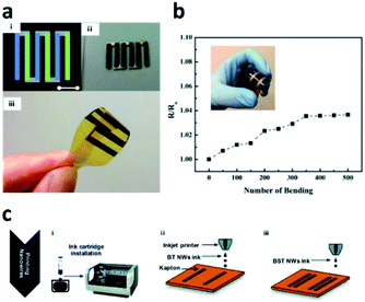 | ||
| Fig. 9 (a) Schematic illustration of printed p–n legs and a flexible device on a PI support. Reproduced from ref. 99 with permission from John Wiley and Sons. (b) Bending tests of the photonic sintered Bi2Te2.7Se0.3 thin films. Reproduced from ref. 119 with permission from John Wiley and Sons. (c) Illustration of the fabrication process of the inkjet-printed TEG device. Reproduced from ref. 9 with permission from the RSC. | ||
Chen et al. also used inkjet printing technology to print bismuth telluride (Bi2Te3) and bismuth antimony telluride (Bi0.5Sb1.5Te3) NWs on a flexible Kapton substrate (Fig. 9c).9 They focused on the thermal annealing process in order to improve the device output to a high level. Finally, maximum power factors of 180 μW m−1 K−2 and 110 μW m−1 K−2 were achieved for Bi2Te3 and Bi0.5Sb1.5Te3 nanowires, respectively. Besides, the maximum power output of their all-printed TEG device can reach 127 nW with a ΔT of 32.5 K as well as high reliability was observed after a bending test.
For example, Kim et al. fabricated flexible TEGs using the screen printing technique (SPT) and a laser multiscanning (LMS) lift-off process. The module has excellent power output (4.78 mW cm−2 and 20.8 mW g−1 at ΔT = 25 °C) even after repeated bending cycles, showing its outstanding stability and deformability (Fig. 10a–c).120 In addition, a flexible pressure/temperature dual-parameter active sensor was produced by Zhu et al. via the screen-printing technique. Fig. 10d shows that the bimodal active sensor has outstanding sensitivity as well as negligible performance degradation after 500 bending cycles.126 This work paves the way toward multifunctional flexible electronics based on PDMS substrates.
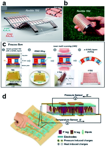 | ||
| Fig. 10 (a and b) Schematic of the flexible TEG produced using the LMS lift-off method. (c) The specific production process for the f-TEG. Reproduced from ref. 120 with permission from American Chemical Society. (d) The working principles of the pressure/temperature dual-parameter active sensor. Reproduced from ref. 126 with permission from John Wiley and Sons. | ||
Kee et al. reported a deformable, self-healing TE module on a PDMS support substrate. In their device, a ternary composite of PEDOT:PSS was mixed with a self-healing material and DMSO additive.122 This TE possesses a unique self-healing property even after stretching and cutting. Moreover, the 3D printed TE material exhibited a power factor as high as 2.5 μW m−1 K−2 and it could retain almost 85% of its maximum value, which is 2.1 μW m−1 K−2 after cutting. This work presents the huge potential of this inimitable characteristic of PDMS as a flexible substrate.
However, the Tg of PDMS is much lower than that of other flexible substrates, which means it is not suitable for those devices with high solder reflow temperature (e.g., Sn–Pb with a solder reflow temperature of 204 °C) and this remains the biggest obstacle for its wide applications.
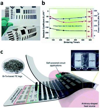 | ||
| Fig. 11 (a) Flexible film on PET produced via screen printing. (b) Variation of σ, S, and S2σ vs. sintering time. Reproduced from ref. 127 with permission from American Chemical Society. (c) Schematic of a flexible thermoelectric generator (TEG). Reproduced from ref. 135 with permission from John Wiley and Sons. | ||
There is no denying that PET and PEN have a high transmittance in the visible range, but the low glass-transition temperature hindered their application. Therefore, it is an urgent need to develop new materials to achieve both high transparency and robust mechanical properties.
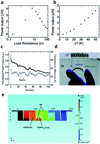 | ||
| Fig. 12 (a) Power output vs. load resistances. (b) Power output vs. temperature differences. (c) Power output and temperature difference versus working time. Reproduced from ref. 102 with permission from the RSC. (d) OTEG on paper with excellent deformability. (e) Potential distribution across the device. Reproduced from ref. 112 with permission from the Royal Society of Chemistry. | ||
| Substrate | Transparency (%) | Glass-transition temperature (Tg, °C) | Young's modulus (GPa) | Flexibility | Stretchability |
|---|---|---|---|---|---|
| PI | — | 410 | 3–4 | Good | Poor |
| PDMS | 92 | 125 | 1–10 | Good | Excellent |
| PET | 90 | 80 | 2.8 | Good | Poor |
| PEN | 87 | 120 | 3.0 | Good | Poor |
| Paper | — | — | — | Excellent | Poor |
| Glass | 90 | 500 | 55 | Poor | Poor |
4.3 Electrodes for TE devices
In addition to the performance optimization of a TE material, the connection between the electrode and the TE material is also one of the key issues in the design and integration of TE devices. The physical properties of the electrode materials (thermal conductivity, electrical conductivity, thermal expansion coefficient) and their compatibility with the TE materials, and the bonding state between the electrodes and the TE materials (bonding strength, interfacial electrical and thermal resistance, chemical stability, etc.) directly affect the efficiency, reliability and service behaviour of TE devices. Particularly for flexible TEG devices, the electrode materials play important roles in their flexibility, internal resistance and Pmax. In PFTE devices, Ag ink or paste is commonly used for electrodes due to its higher conductivity, lower curing temperature and high adaptability to various printing methods. Generally, Ag electrodes can fulfill the requirements for connecting most of the organic TE materials. However, for a variety of inorganic TE materials with much higher electrical conductivities, such as Bi2Te3-based materials, silver electrodes may not be the best choice. It is reported that the contact resistance between Ag electrodes and painted Bi2Te3-based TE legs is three or four orders of magnitude higher than that observed in typical Cu/Bi2Te3 systems.136 The electrical connection between a Ag electrode and a TE leg coated with Bi2Te3 is shown in Fig. 13a and b. Therefore, developing conductive inks or pastes suitable for different TE systems could effectively boost TE device performances.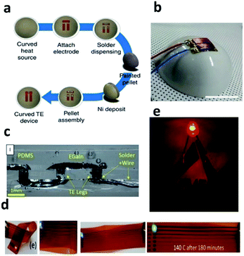 | ||
| Fig. 13 (a and b) Ag is used as an electrode to make a TE generator. Reproduced from ref. 136 with permission from Springer Nature. (c) Bulk TE leg with EGaIn liquid metal as the electrode. Reproduced from ref. 138 with permission from Elsevier. (d) Functional LED with thin copper traces (<1 μm) as electrodes. Reproduced from ref. 140 with permission from American Chemical Society. (e) The printed graphene ink is conductive. Reproduced from ref. 142 with permission from John Wiley and Sons. | ||
Wang et al. have utilized printable Sn96.5Ag3Cu0.5 paste and Sn42Bi58 paste to assemble p-type Bi0.5Sb1.5Te3/n-type Bi2Se0.5Te2.5 unicouples onto a flexible printed circuit board (FPCB), as hot-side and cold-side contact materials, respectively.137 By virtue of the lowered contact electrical and thermal resistance, the fabricated FTE devices possess a very low internal resistance of 1.8 Ω, and a relatively high Pmax when ΔT = 50 K, which are superior to those of the devices previously assembled using silver paste.
Kim et al.120 fabricated a flexible TEG device composed of screen-printed Bi0.3Sb1.7Te3 (p-type) and Bi2Se0.3Te2.7 (n-type). They used Sn-based solder paste instead of Ag paste as the electrodes. The improved performance of the device was partially ascribed to the reduction of the contact resistance between the TE film and solder material.
Besides the conductive inks/pastes, EGaIn liquid metal is also a promising electrode material for PFTE devices due to its very low electrical resistance, excellent flexibility and even the self-healing stretchability. Suarez et al. first used EGaIn liquid metal to connect bulk TE legs embedded in a flexible PDMS substrate (Fig. 13c). A system ZT of 0.35 at a fill factor of 6% was observed for their proof-of-concept devices.138 Furthermore, the devices are mechanically robust with no change in resistance after 1000 bending cycles to a radius of 5 mm. Then, Chen et al.9 used spray-printed EGaIn for connecting the TE legs of inkjet-printed Bi2Te3 and Bi0.5Sb1.5Te3 nanowires in series, which enabled a fully-printed flexible TEG with relatively high Pmax and excellent flexibility.
Although current research on electrode materials in PFTE devices is still quite limited, due to the recent development in conductive inks or pastes, such as inks/pastes containing Cu nanowires, Cu molecules (Fig. 13d), carbon nanotubes, and graphene (Fig. 13e), they may be considered as promising candidates to guarantee better electrical and thermal contact with diverse inorganic TE materials or future organic TE materials with high electrical conductivities.139–142
5. Printing methods
5.1 Inkjet printing
The inkjet printing technique is developing rapidly towards intelligence, simplicity and personalization. Due to the different working principles, inkjet printing can be categorized into the continuous inkjet-printing method and the on-demand inkjet-printing method. The continuous inkjet-printing method involves a pumping control process, after which an oscillator is used to actuate the nozzle to eject continuous droplets with the same volume and pitch. These droplets are then selectively charged as they pass through the nozzle. Under the action of voltage, the charged droplets will be ejected to the substrate according to the predesigned track while the uncharged ones will enter the circulation back to the cartridge for repeated use.143 There are two operating principles for the on-demand inkjet printing method depending on different printheads. One is the thermal printhead mode and the other is the piezoelectric printhead mode. TE material inks are mostly printed with a piezoelectric printhead which is compatible with organic inks. To deposit fine patterns of TE materials by the inkjet printing method, the viscosity and tension of the ink should be rationally optimized.144 When a piezoelectric printhead is used, the piezoelectric material can produce different ink deformations according to the changes of the applied voltage signal, therefore completing the nozzle's absorption and spraying of droplets. By adjusting the drive waveform, the ink droplets can be ejected in the same amount and direction each time to achieve precise control of the droplet size. In addition, the morphology of the ink droplets is also related to the piezoelectric sheet. In principle, a smaller piezoelectric sheet enables lower volume of ink droplets. With the continuous development of the specification of equipment, inkjet printing technology has attracted great attention in the field of scientific research, such as biosensors, solar cells, TE devices, etc.145–148Bismuth telluride (Bi2Te3) based alloy, known as the earliest discovered compound semiconductor TE material, has been proved to be compatible with inkjet printing technology. Compared with other conventional methods for the fabrication of thin film TE devices, such as vacuum evaporation, pulsed laser deposition, etc., functional inkjet printing is more widely applied for quick and large-scale production at low cost. Lu et al.,99 for the first time, proposed a method to fabricate whole thin film TE devices on both glass and PI substrates based on p-type Sb1.5Bi0.5Te3 nanoparticles and n-type Bi2Te2.7Se0.3 nanoparticles via inkjet printing. Chen et al.9 also printed Bi2Te3 and Bi0.5Sb1.5Te3 NWs as n-type and p-type legs, respectively, to prepare TEGs, and achieved a maximum PF of 1.8 × 10⁻⁴ W m−1 K−2. It is worth mentioning that after fifty bending experiments around a radius of curvature of 11 millimetres, the performance showed no decline, which offers a glimpse of the possibility of using inkjet printing technology in wearable TE device preparation.
However, the toxicity of traditional Bi–Te alloys hinders their application in inkjet-printed wearable TEGs. Many efforts have been made to find appropriate alternative materials to make FTE devices more environmentally friendly.149 Here, nanoscale carbon-based and organic hybrid materials will be introduced. Horike et al.,150 precisely prepared p-type and n-type SWCNTs using the inkjet printing method. By introducing poly(vinyl acetate) (PVA) as a doping material, a module consisting of two units of p-type and n-type SWCNTs was formed successfully on the substrate of quartz glass with increased TE voltage for each leg. No separate deposition steps or additional electrodes were required for later applications. Juntunen et al.100 reported inkjet-printed large-area flexible graphene films with prominent TE properties. Owing to the phonon-glass electron-crystal character, the prepared all-graphene film showed a TE PF of 18.7 μW m−1 K−2 at RT, which is threefold improvement compared to that of the all-graphene devices prepared via solution processing (Fig. 14). By tuning the ratio of additive PVP in graphene ink, they successfully obtained n-type and p-type charge transport in the same process. The improved recipe of ink resulted in outstanding thermal stability and durability against mechanical deformation for over 10![[thin space (1/6-em)]](https://www.rsc.org/images/entities/char_2009.gif) 000 bending cycles.
000 bending cycles.
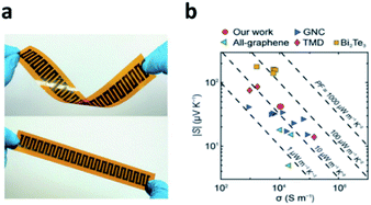 | ||
| Fig. 14 (a) Graphs of a flexible inkjet-printed device. (b) Performance comparison of the present work and other large-area solution-processed materials. Reproduced from ref. 100 with permission from John Wiley and Sons. | ||
Organic and hybrid materials have come into view as non-toxic and low-cost alternatives in recent years. Combined with inkjet printing technology, organic and hybrid materials show great potential in the field of flexible large-area TEGs. Ferhat et al.128 first introduced nanocomposite hexylammonium titanium disulfide (TiS2(HA)x) to form the n-type component, and PEDOT:PSS as the p-type component. As a result, organic TEGs composed of these two materials were patterned via inkjet printing technology on a flexible paper substrate. Owing to the outstanding TE properties of both TiS2(HA)x and PEDOT:PSS, the printed device with seven thermocouples patterned as an asymmetrical π-shaped structure showed a maximum power output of 22.5 nW in a small area of 128 mm2 at a near ambient temperature difference of 20 K, demonstrating a strong level of competition against many other state-of-the-art thin flexible devices in a similar working environment.
5.2 Screen printing
Screen printing is widely considered as one of the most mature printing technologies due to its years of development in the electronics industry. Basic screen printing consists of five main elements: screen mask (stencil), squeegee, press bed, printing ink and substrate.151 During the printing process, a pre-designed ink is poured onto the stencil, and squeegeed with certain pressure getting in touch with the substrate at the bottom through the screen mask. As the screen and the substrate maintain a certain gap, pressing on the screen produces a reaction force on the squeegee, which is called rebound force. Under the action of the rebound force, the contact line between the stencil and the substrate moves along the printing direction, while other parts of the stencil and the substrate remain detached, leading to the separation of the ink and the stencil and ensuring the accuracy of printing size and the tidiness of the substrate. When the squeegee scrapes the entire substrate, the squeegee and the stencil are lifted and the ink is lightly scraped back to the initial position, which completes a printing cycle (Fig. 15a). Screen printing technology is more suitable for large-scale industrial production due to its simple and low-cost preparation process. It can also achieve the objective of multiple printing cycles on demand to regulate the thickness of the film. Due to these unique merits, screen printing technology has won a great honour among numerous printing methods.152,153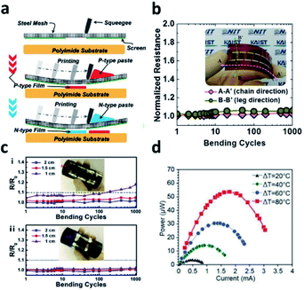 | ||
| Fig. 15 (a) Fabrication process of screen printing technology. Reproduced from ref. 154 with permission from Elsevier. (b) Changes of the device resistance with a bending radius of 4 cm. Reproduced from ref. 155 with permission from Elsevier. (c) Changes of TEG resistance as a function of bending cycles under longitudinal and transverse directions with different bending radii of curvature. Reproduced from ref. 33 with permission from Elsevier. (d) Power output versus electrical current at various gradients of temperatures. Reproduced from ref. 134 with permission from John Wiley and Sons. | ||
J. Weber et al.156 for the first time demonstrated a Bi2Te3 based micro TEG prepared on PI flexible substrates by screen printing technology, and realized a wearable TEG device using the human body as a heat source. Limited by the low quality of the printing film which contained many vacancies and low density, the output power of the device was only 1.2 μW at a temperature gradience of 10 K. However, this work still reveals the feasibility of depositing TE materials by the screen printing method. All-inorganic semiconductor alloy materials based on Bi2Te3 still suffer from their brittleness property. In response to this problem, multiple kinds of polymer materials have been proposed to enhance the quality of flexible films in the screen printing process. For instance, We et al.155 introduced PEDOT:PSS as a filler to fix the micropores in the screen-printed film, combined with the spin coating method and infiltration process. The flexibility of the TE device was significantly improved without degrading the TE performance, as shown in Fig. 15b. Yuan et al.154 designed a screen printing paste composed of TE powder (i.e., p-type Bi0.5Sb1.5Te3, Sb2Te3 and n-type Bi2Te2.7Se0.3) and an epoxy system (i.e., polypropylene glycol diglycidyl ether epoxy resin and the methylhexahydrophthalic anhydride). Upon regulating the curing temperature, the performance of the micro radioisotope TEG demonstrated that under 300 °C, the p-type and n-type TE legs screen-printed on the 75 μm PI substrate have electrical conductivities of 165.8 and 39.89 S cm−1 with Seebeck coefficients of 139.7 and −176.6 μV K−1, which were better than those of the previous TEG devices at that time. After that, they also developed a microstacked-integrated annular-radial TEG and achieved a maximum series voltage of 2.2 V for 30 layers.157
It is acknowledged that the power factor is highly related to the curing temperature of the TE materials. Kim et al.129 screen printed Bi2Te3 (n-type) and Sb2Te3 (p-type) on glass fabric, and both TE films were annealed at over 500 °C to guarantee a better performance. However, for most flexible substrate materials, excessively high sintering temperatures may lead to changes in their mechanical properties, thereby destructing the bendability of the FTE devices. By now, numerous efforts have been made to improve the subsequent sintering process in screen printing technology. Chang et al. fabricated a flexible TEG using screen printing in conjunction with pressurized sintering techniques.33 After sintering at 345 °C with a pressure of 25 MPa, the printed films Bi–Sb–Te (p-type) and Bi–Se–Te (n-type) exhibited power factors of 14.3 and 8.4 μW cm−1 K−2, respectively. Slight degradation of the resistance is shown in Fig. 15c. Varghese et al. demonstrated a novel strategy.134Via a tellurium-based nanosolder approach, the interfaces of TE particles could be efficiently bridged, so that the charge carrier mobility of the printed films was dramatically enhanced. As a result, the fabricated p-type film based on Bi0.4Sb1.6Te3 nanoparticles showed a TE PF of 3 mW m−1 K−2 and a ZT of about 1 at RT with excellent flexibility. Fig. 15d shows the correlative power output under different temperature gradients. Even screen printing technology has become one of the most mature printing methods, and more studies have to be focused on several perspectives, for instance, the solutions towards the rough surface of the printed films, the possible component volatilization during sintering, low density caused by vacancies, etc.
5.3 3D printing
The 3D printing technology, also named additive manufacturing technology, is a combination of quick prototyping systems and computer data models that can manufacture many complex industrial products without the requirement of any additional conventional mold making of the machining process. The 3D printing process basically covers three main parts: modeling, printing, and completion. A 3D printed model can be generated on a computer using software or with the participation of a 3D scanner. The geometric data needed for 3D images are collected manually, in a process similar to that of plastic arts such as sculpture. A 3D scanner can also be used to create a 3D model of the related object. Even though many other printing methods, such as inkjet printing and screen printing, optimize the TE fabrication by enlarging the size of the printable area, 3D printing technology has its unique advantages of the ability to target the manufacturing, particularly in the lengthwise direction, realizing high accuracy and on-demand fabrication with specific shapes. Since it was first invented,158 3D printing technology has been rapidly developing in recent years with the improvement of the manufacturing industry, and tremendous research studies have been reported in the field of bionics, electronics, medical and materials science, etc.159–163 Because of the close interaction with simulation and calculation, more theoretical innovations are demanded for the development of 3D printing technology.Normally, the 3D printing method covers several techniques in terms of fabrication of TE materials, stereolithography apparatus, fused deposition modelling, selective laser melting/sintering, and solution printing.164 The first practical TE application was reported by He et al. via stereolithography apparatus technology.165 Owing to its merit of producing individual TE objects, they reported the successful fabrication of p-type TE materials which contained Bi0.5Sb1.5Te3 and a regulated photoresin via 3D printing technology. However, due to the extremely low electrical conductivity of resin-based materials, the ZT value only reaches 0.12. To overcome this, it is necessary to choose suitable 3D printing materials with high TE performance.
By now, PFTE devices are mainly fabricated with the aid of solution printing technology. During the printing process, functional inks of polymers, inorganic–polymer hybrid materials and inorganic materials could be printed layer by layer to obtain samples with various thicknesses. Kee et al. developed a p-type TE ternary composite ink containing PEDOT:PSS as a surfactant, Triton X-100 as a healing agent, and DMSO as a TE performance booster.80 The corresponding TE film was reported to present both stretchability and self-healing ability. The TEG prepared by this special ink via 3D printing technology showed a maximum power output of 12.2 nW, owing to the self-healing ability, and the process is shown in Fig. 16. More than 85% of the initial power output can be retained after multiple times of cutting. Du et al. first demonstrated an n-type TE material composited with tungsten carbide and polylactic acid (WC/PLA) for the solution printing process.166 By tuning different volume ratios of WC, the improvement of the Seebeck coefficient and electrical conductivity can be achieved, with maximum values of −12.3 μV K−1 and 42.2 S cm−1, respectively, and the maximum ZT value was ∼6.7 × 10⁻⁴ when the volume ratio of WC was 60%. The flexibility was shown via 300 bending experiments, and the ZT value for 5% volume ratio of WC remained unchanged in a relatively low level. They also found that the flexibility was inversely proportional to the content of WC. In order to achieve FTE materials with higher ZT values using solution printing technology, they later developed flexible ternary composites with carbon black/Bi2Te3 based alloy/polylactic acid (CB/BTBA/PLA) (Fig. 17).69 Compared with former research, the introduction of BTBA can significantly increase the Seebeck coefficient and electrical conductivity, leading to an improvement of the ZT value. Besides, carbon black is much cheaper than WC conducting fillers. As a result, the TE performance can be optimized to a ZT value of 0.023 at 300 K, showing great application prospects in FTE devices.
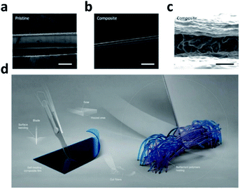 | ||
| Fig. 16 Self-healing process in viscoelastic TE composites. Scanning electron microscopy (SEM) images of (a) the PEDOT:PSS film without a surfactant and (b) the composite film on a glass support substrate. The scale bar is 50 μm. (c) Magnified SEM image of a cut on the composite film. Scale bar, 5 μm. (d) Schematic illustration of the mechanical and thermoelectrical self-healing process. Reproduced from ref. 80 with permission from John Wiley and Sons. | ||
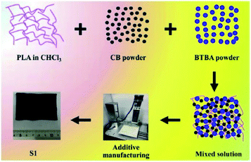 | ||
| Fig. 17 Schematic of the fabrication process of the CB/BTBA/PLA TE composites via SP technology. Reproduced from ref. 69 with permission from Elsevier. | ||
5.4 Other printing methods
Except for the above three printing methods, other methods such as aerosol jet printing, R2R printing, brush printing, etc. are applied in the preparation of different TE materials (Fig. 18).167 Aerosol jet printing technology is based on an atomizer which can transform the ink into liquid particles with a size of approximately 20 nm to 5 μm, and then the particles are sprayed onto the substrate using inert gas or compressed air stream. Aerosol jet printing technology presents higher resolution than inkjet printing technology; however, the sheath gas may also induce detrimental side-effects.34 Zhang et al. printed Bi2Te2.7Se0.3 nanoplates via aerosol jet printing combined with a rapid photonic sintering method.119 The prepared films exhibited an electrical conductivity of 2.7 × 10⁴ S m−1. R2R printing technology is a continuous printing technology working similarly to screen printing technology. The advantage of high throughput makes it an important production tool for the mass manufacturing process. However, the study about R2R printed TE materials is still in its infancy. Zhang et al. fabricated a wearable TEG based on n-type and p-type SWCNTs/PEDOT:PSS composites, and obtained a voltage output of 20 mV with 20 p–n junctions.168 Brush printing, commonly regarded as an easier method with low cost, is applied using a predesigned template and brushes. However, its low resolution and printing speed are the main concerns in the application of TE devices. Park et al. demonstrated brush-printed n-type and p-type TE materials with Sb2Te3-based TE devices with ZT values of 0.67 and 1.21, respectively, and achieved an output power of 4.0 mW cm−2.136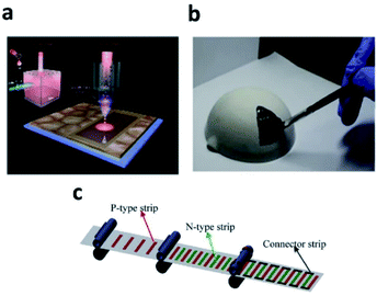 | ||
| Fig. 18 (a) Aerosol jet printing technology. Reproduced from ref. 169 with permission from John Wiley and Sons. (b) Brush printing technology. Reproduced from ref. 170 with permission from Springer Nature. (c) Roll-to-roll printing technology. Reproduced from ref. 136 with permission from Elsevier. | ||
6. Devices and applications
6.1 TEG
The structure of a TEG is mainly divided into two categories. The first is the planar TEG (the substrate and the junction in the TEG are on the same plane), and the second is the through-TEG (the TEG junction is not on the substrate surface, but in the cross-sectional direction of the substrate). For wearable TE devices, the heat source of the human body is a plane heat source. Therefore, researchers have proposed design schemes for generating temperature differences on a planar heat source, such as folding,171 origami102 and other design methods. Here, the focus is on the performance of TEG devices prepared using printing technology.Mukaida et al. prepared paper-based TE devices, by connecting 300 sheets of paper through copper plates or wires, and the energy generated after using a boost converter could provide electricity for LEDs (ΔT = 100 K). After the hot pressing process was improved, the device achieved an output power of 37 μW (ΔT = 50 K).172
Bae et al. proposed another novel folded TEG structure, which uses a distributor to print a TEG on a flexible base.173 This is a through-TEG, and the junction of TEG is perpendicular to the substrate plane (Fig. 19a and b). When the temperature difference was 10 K, an output power of 10.59 nW was achieved.
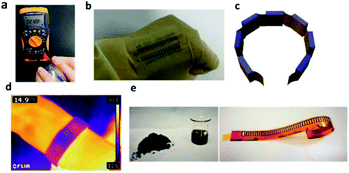 | ||
| Fig. 19 (a and b) Foldable TEG that uses human body heat to generate electricity. Reproduced from ref. 173 with permission from Springer Nature. (c and d) Wristband wearable TEG. Reproduced from ref. 65 with permission from Elsevier. (e) The picture on the left shows the dry powder and dispersion of B-SWCNTs, and the picture on the right shows the flexible TEG printed with B-SWCNT ink. Reproduced from ref. 71 with permission from American Chemical Society. | ||
Zeng et al. fabricated a flexible TE generator by assembling an rGO film on a 3D printed PDMS grid (Fig. 19c and d), and its output voltage per unit mass was 57.33 mV g−1 when ΔT = 50 K.65 The wristband-type flexible TE generator has 7 pairs of thermocouples, which exhibited a maximum power density of 4.19 μW g−1 at an ambient temperature of 15 °C. This simple and controllable 3D printing technology can be used in more energy conversion devices such as wearable TE devices and temperature sensors.
Liu et al. used boron-doped single-walled carbon nanotubes (B-SWCNTs) to improve the Seebeck coefficient and conductivity of SWCNTs.71 Therefore, using B-SWCNT dispersion and silver paste as materials, a printable TEG with a length of 253 mm was fabricated on a PI substrate (Fig. 19e). The generator is composed of 61 single pairs of p-type legs. When ΔT = 60 K, the maximum output voltage and power output reached 20 mV and 400 nW, respectively.
Wang et al. used the controllable compensation power of Te to enhance the TE performance of n-Bi2Te3 and p-Sb2Te3 in the manufacturing process.174 At RT, the conductivity, Seebeck coefficient and power factor of n-Bi2Te3 are 5.12 × 10⁴ S m−1, 130.38 μV K−1, and 8.71 μW cm−1 K−2, respectively. In comparison, the conductivity, Seebeck coefficient and power factor of p-Sb2Te3 are 10.49 S m−1, 133.05 μV K−1, and 18.58 μW cm−1 K−2, respectively. They integrated a conductive elastomer-based pressure sensor with a flexible thin film TEG to collect human body heat and developed a self-powered wearable pressure sensing system. The system realized continuous monitoring of human physiological signals and human motion for the first time without the need of an electronic booster circuit (Table 3).
| Materials | Printing method | Output power/power density | ΔT (K) | Ref. |
|---|---|---|---|---|
| PEDOT:PSS | Screen printing | 24 μW cm−2 | 50 | 172 |
| Bi2Te3 and Sb2Te3 | Dispenser printing | — | — | 175 |
| p-Type CNT–polystyrene | Screen printing | 55 mW m−2 | 70 | 176 |
| Bi and Bi0.5Sb1.5Te3 | Dispenser printing | 1230 μW cm−2 | 70 | 177 |
| Polymer based | Brush painting | 0.015 μW cm−2 | 45 | 178 |
| BiTe/SbTe | Screen printing | 0.012 μW cm−2 | 20 | 179 |
| Polymer-based | Dispenser printing | 0.001 μW cm−2 | 10 | 173 |
| Bi2Te2.8Se0.2 | Screen printing | 4.1 mW cm−2 | 60 | 19 |
| p-Type Bi2Se0.3Te2.7 | Dispenser printing | 10 nW | 35 | 180 |
| p-Type Bi0.5Te1.5Te3 NWs | Inkjet printing | 127 nW | 32.5 | 9 |
| Reduced graphene oxide | 3D printing | — | 50 | 65 |
| Bi2Te2.7Se0.3, p-type Bi0.5Sb1.5Te3 and p-type Sb2Te3 | Screen printing | 5.81 μW cm−2 | — | 181 |
| n-Type SWCNT and p-type SWCNT | Fully printing | 258 μW | 150 | 182 |
| 308 μW | ||||
| n-Type Bi2Te2.7Se0.3 and p-type Bi0.5Sb1.5Te3 | Screen printing | 6.32 mW cm−2 | 25.6 | 183 |
| n-Type (0.98Bi,0.02Sb)2(0.9Te,0.1Se)3 and (0.25Bi,0.75Sb)2(0.95Te,0.05Se)3 | Dispenser printing | 23.9 mW | 22.5 | 184 |
| n-Type Bi1.8Te3.2 and p-type Sb2Te3 | Screen printing | 455.4 nW | 20 | 185 |
| PEDOT NWs and TiS2:hexylamine | Screen printing | 47.8 μW cm−2 | 30 | 103 |
| MA n-type Bi2Te3-epoxy | Dispenser printing | 25 μW | 20 | 186 |
| n-Type Bi2Te3 and p-type Sb2Te3 | Screen printing | 28 mW g−1 | 50 | 187 |
6.2 TEC
With the development of wearable and implantable electronic devices, in addition to flexible TEGs, flexible TEC devices have also attracted widespread attention. TECs are based on the Peltier effect to achieve electrical cooling. Direct current is passed into the TEC circuit, and heat will be transferred from one side of the device to the other, thereby producing hot and cold surfaces with different temperatures.188 Therefore, one of the advantages of TECs is that the power of the Peltier device can be adjusted by directly changing the magnitude of the input current. Vera-Marun et al. regarded two-dimensional graphene as an excellent nano-scale carbon material, and explored the interaction between electrons and heat transfer phenomena.189 Thanks to the architecture that includes a nanometer thermometer, when T = 300 K, after inputting a current of 20 μA, a Peltier component modulation with a ΔT of 15 mK was measured, and it was observed that the Peltier cooling and heating of electrons and holes are completely opposite states, which provided a new avenue for the study of 2D nano-scale TE materials. Hu et al. combined highly controllable nanobubble technology to construct a flexible graphene wrinkle multifunctional platform (Fig. 20a).190 The Peltier effect was improved by controlling the current flowing through the wrinkles. This is the first time that the Peltier effect of graphene wrinkles has been observed by scanning thermal microscopy (SThM), which makes it possible to cool 2D nanoelectronic chips with van der Waals junctions.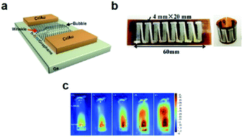 | ||
| Fig. 20 (a) Schematic diagram of graphene wrinkles embedded in nano-shrinkage. Reproduced from ref. 190 with permission from Springer Nature. (b) Flexible TEC made of a Bi0.5Sb1.5Te3/epoxy thick film. Reproduced from ref. 67 with permission from Springer Nature. (c) Infrared images of the composite thick film measured at different currents. Reproduced from ref. 68 with permission from John Wiley and Sons. | ||
Jin et al. fabricated a poly(Ni-ett)-based organic TEC on an ultra-thin (300 nm) suspended parylene film with excellent mechanical properties, which has a large ΔT (∼38 ± 3 K) at a current density of 5 A mm−2.191 Under adiabatic conditions, at a current density of 0.1 A mm−2, there is also a temperature difference of 0.2 K. In addition, Hou et al. used a Bi0.5Sb1.5Te3/epoxy resin thick film to fabricate a flexible TEC device with a thermo-compression curing process (Fig. 20b).67 The device achieved a stable temperature difference of 6.2 K at a working current of 0.06 A. Zhao et al. used screen printing technology to prepare a flexible Bi0.5Sb1.5Te3/epoxy composite flexible TE thick film on a polyimide substrate.68 It can be seen from the infrared image that the temperature difference established by the composite thick film is different when different currents are applied (Fig. 20c). The flexible TE leg can establish a temperature difference of 4.2–7.8 K under the working current of 0.01–0.05 A. Hng et al. synthesized p-type Sb1.5Bi0.5Te3 and n-type Bi2Te2.7Se0.3 nanoparticles, and used inkjet printing technology to print local coolers on PI substrates.99 This local cooler may be used in microelectronics. It has application potential in terms of heat dissipation. As we know, there are many reported studies on flexible TEGs, but the flexible Peltier refrigeration, particularly printable flexible Peltier devices, has also attracted great research interest in recent years (Table 4).
6.3 TES
TEGs used for flexible sensors, which can efficiently detect different stimuli relevant to specific environmental or biological species, have been widely studied owing to their bright future in wearable electronics, biomedical monitoring, and artificial intelligence applications.22,45,113,123,129,132,148,192In 2007, Leonov et al. demonstrated a TEG-based sensor, and the output power density can exceed 20 μW cm−2.193 More importantly, the device is the initial attempt to collect human body heat for self-powered sensors. In 2017, Han et al. reviewed the state-of-the-art flexible sensors.192 They paid great attention to printed flexible sensors, particularly for temperature and humidity-based devices. They also put forward flexible sensors which aimed at serving the human body, and the biocompatibility of the components and conformable supports are the key issues. Therefore, we think printing technologies in conjunction with TEGs could have a place in the field of sensors due to their super-sensitivity and high compatibility.
In the work of Wang et al., they combined a conductive pressure-induced sensor with flexible thin-film TEGs.125 The thin-film TEG based on a Bi2Te3 thin film was imbedded in a deformable PDMS/boron nitride (BN) composite film (Fig. 21c and d). They used hydrogel as the heat sink. The temperature gradient can be maintained with long-term stability. This device could collect the human body heat to activate the pressure sensor function subsequently. Finally, the dedicated thermal–pressure detection system exhibited high sensitivity, fast response time and superior reliability even after 3000 cycles (Fig. 21c and d). In addition, Ruan et al. used a traditional wet spinning technique to manufacture a flexible hollow PEDOT:PSS fiber.194 The device output a summit voltage of 404 μV with 5 legs as well as showed long-term stability in the ambient atmosphere. This work may provide a novel approach for wearable electronics.
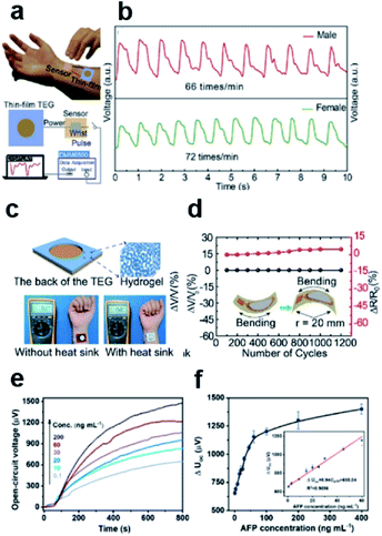 | ||
| Fig. 21 (a) Wrist pulse monitoring with a self-powered pressure sensing system. (b) Wrist pulse signal output. Reproduced from ref. 125 with permission from Elsevier. (c) Schematic of the tf-TEG and the power output with/without hydrogel heat sink. (d) Performance reliability of the tf-TEG under 1200 bending cycles. Reproduced from ref. 125 with permission from Elsevier. (e) Open-circuit voltage vs. time for different AFP concentrations. (f) Open-circuit voltage vs. AFP concentration. Reproduced from ref. 82 with permission from American Chemical Society. | ||
In addition to the TEG powered TESs, there are also sensors directly utilizing the voltage signals induced by TE effects. For example, Huang et al. produced an FTE component in a self-powered temperature sensor.82 They introduced GOx conjugated secondary antibodies into an immunoassay, so the degradation of the photothermal materials could speed up (Fig. 21c and d). Therefore, the photothermal product could be used to determine AFP (α-fetoprotein) qualitatively. They supposed this strategy has great potential for application in clinical diagnosis and the unique ideas could inspire the development of traditional TEGs. However, the complicated device structure and fabrication process may be an obstacle for commercial application; meanwhile, the device stability is still a problem to be solved.
Zhang et al.195 manufactured flexible temperature–pressure bifunctional sensors using PEDOT:PSS and porous polyurethane (PU) frames (MFSOTE). The prepared sensors took advantage of the Seebeck effect of PEDOT:PSS and the pressure-induced current change of the MFSOTE material, enabling a high-temperature detection resolution and pressure-sensing sensitivity of 0.1 K and 27.9 kPa−1, respectively. Furthermore, they fabricated a 12 × 12 pixel MFSOTE array on a 500 μm thick fabric glove with a stamp-printing method (shown in Fig. 22a) and demonstrated its application as artificial electronic skin, which light up the future application of PFTE devices in robotics and health-monitoring products. More recently, Deng et al.126 constructed an all-organic 3D architectured pressure/temperature bimodal active sensor (Fig. 22b) using a combined laser fabrication and screen-printing method, which can transform pressure and temperature stimuli into independent electrical signals with high sensing sensitivities. A full-fabric self-powered temperature–pressure sensor was reported by Chen et al.196 and was used in a waistcoat for the first time.
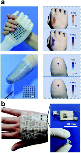 | ||
| Fig. 22 (a) Demonstration and performance of flexible MFSOTE matrixes. Reproduced from ref. 195 with permission from Springer Nature. (b) Photographs of the bimodal sensor array and its enlarged images. Reproduced from ref. 126 with permission from John Wiley and Sons. | ||
In fact, besides temperature sensing, thermoelectric materials can also be used in diverse sensing scenarios, such as gas sensing197–199 and infrared (IR) radiation detection.200 K. Rajanna et al.198 manufactured acetone gas sensors based on SnO2 films with a Pt catalyst using DC magnetron sputtering techniques. When passing through the sensor, acetone gas will undergo an exothermic reduction reaction on the Pt catalyst and generate a temperature difference on the SnO2 film, which leads to an output voltage. Thus, the concentration of acetone gas in the environment can be qualitatively determined. Hydrogen and oxygen detectors can also be developed using similar principles.197,199 In addition, micro-electromechanical system (MEMS)-based thermoelectric IR sensors are also some of the important applications for thermoelectric materials. Xu et al.200 reviewed the recent progress in this area, which is suggested for further reading. Although flexible gas sensors and infrared detectors prepared by printing methods have not been reported yet, with the development of printing thermoelectrics and the application of flexible electronics, related devices can still be expected.
Even though TE-based sensors have great potential in terms of artificial intelligence, wearable electronics and immunoassay electronic devices, the intrinsic low power output and complicated device configuration remain tough problems to tackle. Therefore, exploiting new materials and printing methods is necessary in the future.
7. Conclusions and outlook
As discussed above, in recent years, the research on PFTE devices, including their related materials, printing methods and device design, has gradually entered a period of prosperity. However, the application of such devices is still in its infancy. On the one hand, the Pmax of most printed flexible TEG devices still stays at the nW level, which is far from the minimum power requirements (μW level) of most of the state-of-the-art microelectronic devices.201 On the other hand, the maximum ΔT produced by the printed flexible TEC devices at a small operating current density is only about tens of mK,202 which is far from meeting the demands of practical applications. In fact, this situation is also a common problem in all FTE devices at present. Some considerations should be taken into account in future research on PFTE devices. First, since most of the PFTE devices work near RT, developing novel TE materials with high ZT near RT should be the most direct and effective way to improve the performance of the devices. Until now, Bi2Te3-based materials are still the most widely used materials for PFTE devices, despite their relatively high costs. The emergence of new room-temperature high-performance TE materials, such as p-type MgAgSb203,204 and n-type Mg3Sb2/Mg3Bi2-based205,206 TE materials, may provide better choices for low-cost PFTE devices. Furthermore, the RT ZT values of these materials are being progressively improved. Second, although organic TE materials have good flexibility and excellent printability, the intrinsically poor electrical transport performance severely limits their application in TE devices, particularly in TEC devices. The research on organic materials for TECs is currently at the stage of how to extract the Peltier effect signal from the overwhelming Joule effect background.207 Therefore, hybridization with inorganic materials is generally the main application form of organic TE materials. Recently, the developments in inorganic TE materials with intrinsic flexibility may provide a new direction for the development of PFTEs. In 2018, Shi et al. discovered the first room-temperature ductile inorganic semiconductor, Ag2S, and revealed its plastic deformation mechanism.208 Subsequently, the same group demonstrated the application of the relevant ductile silver chalcogenides in full-inorganic FTE devices, after optimizing their electrical transport properties.209 Recently, He et al. discovered a series of amorphous TE materials in the Ag2Te–Ag2S system.210 In addition to the low thermal conductivity that belongs to their innate properties, this series of amorphous TEs have extremely high RT carrier mobility up to ∼750 cm2 V−1 s−1 at a carrier concentration of 8.6 × 1018 cm−3, which guarantees a large PF of ∼5.7 μW cm−1 K−2. In addition to the impressive TE properties of the above-mentioned inorganic materials, their excellent flexibility and processability enable them to act as active components or functional substrates for the preparation of free-standing PFTE devices in the future, which may greatly simplify the preparation process and reduce the cost of the devices, while improving their performance. Third, during the working process of TE devices, it is of great importance to maintain the temperature difference between the hot- and the cold-side, which should be seriously considered in the design of FTE devices. Besides minimizing the thermal conductivity of the TE materials, reducing the thermal resistance at both ends of the device and optimizing the device structure are also crucial aspects. More importantly, in the design of wearable PFTE devices, if the TE functional components can be integrated with other flexible electronic components to form a functional chip similar to the System on Chip (SoC) architecture, it is possible to greatly reduce the electrical and thermal loss and thus improve the overall efficiency of the devices. In summary, the fascinating advantages of PFTE devices will certainly attract more and more investments and research interest from industry and academia, which may provide more opportunities to realize high-performance, low-cost PFTE devices in the near future and greatly extend the application scope of TEs.Author contributions
Jiaqing Zang: writing, literature review, summarization of modifications & characterization. Jiayi Chen: writing, literature review, manuscript modification. Zhewei Chen: writing review, comment & editing. Ya Li: writing review, comment & editing. Jiye Zhang: writing review, editing, manuscript modification. Tao Song: editing, supervision, project administration. Baoquan Sun: funding acquisition & supervision.Conflicts of interest
There are no conflicts to declare.Acknowledgements
We would like to acknowledge the National Natural Science Foundation of China (52072234, 91833303, 61974098), Open Project of Jiangsu Key Laboratory for Carbon-Based Functional Materials & Devices (KJS2023), Collaborative Innovation Center of Suzhou Nano Science & Technology (CIC), the 111 Project and Joint International Research Laboratory of Carbon-Based Functional Materials and Devices.References
- M. Nishibori, W. Shin, N. Izu, T. Itoh and I. Matsubara, Sens. Actuators, B, 2009, 137, 524 CrossRef CAS
.
- X. B. Wang, P. F. Qiu, T. S. Zhang, D. D. Ren, L. H. Wu, X. Shi, J. H. Yang and L. D. Chen, J. Mater. Chem. A, 2015, 3, 13662 RSC
.
- J. Mao, G. Chen and Z. F. Ren, Nat. Mater., 2021, 20, 454 CrossRef CAS PubMed
.
- J. Y. Zhang, J. H. Zhu, L. You, K. Guo, Z. L. Li, W. G. Lin, J. Huang and J. Luo, Mater. Today Phys., 2019, 10, 100095 CrossRef
.
- J. He and T. M. Tritt, Science, 2017, 357, eaak9997 CrossRef PubMed
.
- L. E. Bell, Science, 2008, 321, 1457 CrossRef CAS PubMed
.
-
M. S. Dresselhaus, Chemistry, Physics, and Materials Science of Thermoelectric Materials, Springer US, Springer Science+Business Media, New York, 2003 Search PubMed
.
- B. Chen, S. R. Das, W. Zheng, B. Zhu, B. Xu, S. Hong, C. Sun, X. Wang, Y. Wu and J. C. Claussen, Adv. Electron. Mater., 2017, 3, 1600524 CrossRef
.
- B. Chen, M. Kruse, B. Xu, R. Tutika, W. Zheng, M. D. Bartlett, Y. Wu and J. C. Claussen, Nanoscale, 2019, 11, 5222 RSC
.
- F. Jiao, C.-a. Di, Y. Sun, P. Sheng, W. Xu and D. Zhu, Philos. Trans. R. Soc., A, 2014, 372, 20130008 CrossRef PubMed
.
- A. Sajedi-Moghaddam, E. Rahmanian and N. Naseri, ACS Appl. Mater. Interfaces, 2020, 12, 34487 CrossRef CAS PubMed
.
- L. J. Guo, X. Cheng and C.-F. Chou, Nano Lett., 2004, 4, 69 CrossRef CAS
.
- X. Guo, J. Li, M. Arabi, X. Wang, Y. Wang and L. Chen, ACS Sens., 2020, 5, 601 CrossRef CAS PubMed
.
- I. Park, S. H. Ko, H. Pan, C. P. Grigoropoulos, A. P. Pisano, J. M. J. Fréchet, E. S. Lee and J. H. Jeong, Adv. Mater., 2008, 20, 489 CrossRef CAS
.
- C. Cao, J. B. Andrews and A. D. Franklin, Adv. Electron. Mater., 2017, 3, 1700057 CrossRef
.
- A. Mahajan, C. D. Frisbie and L. F. Francis, ACS Appl. Mater. Interfaces, 2013, 5, 4856 CrossRef CAS PubMed
.
- G. E. Jabbour, R. Radspinner and N. Peyghambarian, IEEE J. Sel. Top. Quantum Electron., 2001, 7, 769 CrossRef CAS
.
- D. A. Pardo, G. E. Jabbour and N. Peyghambarian, Adv. Mater., 2000, 12, 1249 CrossRef CAS
.
- T. Varghese, C. Hollar, J. Richardson, N. Kempf, C. Han, P. Gamarachchi, D. Estrada, R. J. Mehta and Y. Zhang, Sci. Rep., 2016, 6, 33135 CrossRef CAS PubMed
.
- M. Berggren, D. Nilsson and N. D. Robinson, Nat. Mater., 2007, 6, 3 CrossRef CAS PubMed
.
- Q. Huang and Y. Zhu, Adv. Mater. Technol., 2019, 4, 1800546 CrossRef
.
- Y. Khan, A. Thielens, S. Muin, J. Ting, C. Baumbauer and A. C. Arias, Adv. Mater., 2020, 32, e1905279 CrossRef PubMed
.
-
H. J. Goldsmid, Thermoelectric Refrigeration, Springer, 1964 Search PubMed
.
- W. Thomson, Proc. R. Soc. Edinburgh, 1857, 3, 91 CrossRef
.
-
D. M. Rowe, CRC Handbook of Thermoelectrics, 1995 Search PubMed
.
- M. S. Dresselhaus, G. Chen, M. Y. Tang, R. G. Yang, H. Lee, D. Z. Wang, Z. F. Ren, J. P. Fleurial and P. Gogna, Adv. Mater., 2007, 19, 1043 CrossRef CAS
.
- Y. Xiong, X. Yu, Y. Huang, J. Yang, L. Li, N. Yang and D. Xu, Mater. Today Phys., 2019, 11, 100139 CrossRef
.
- Y. Li, Q. Meng, Y. Deng, H. Zhou, Y. Gao, Y. Li, J. Yang and J. Cui, Appl. Phys. Lett., 2012, 100, 231903 CrossRef
.
- K. Biswas, J. Q. He, I. D. Blum, C. I. Wu, T. P. Hogan, D. N. Seidman, V. P. Dravid and M. G. Kanatzidis, Nature, 2012, 489, 414 CrossRef CAS PubMed
.
- S. Bhattacharya, A. Bohra, R. Basu, R. Bhatt, S. Ahmad, K. N. Meshram, A. K. Debnath, A. Singh, S. K. Sarkar, M. Navneethan, Y. Hayakawa, D. K. Aswal and S. K. Gupta, J. Mater. Chem. A, 2014, 2, 17122 RSC
.
- Y.-L. Pei, J. He, J.-F. Li, F. Li, Q. Liu, W. Pan, C. Barreteau, D. Berardan, N. Dragoe and L.-D. Zhao, NPG Asia Mater., 2013, 5, e47 CrossRef CAS
.
- S. S. Pan, C. Y. Wang, Q. D. Zhang, B. Yang, Y. Cao, L. Liu, Y. Jiang, L. You, K. Guo, J. Y. Zhang, J. Yang, J. Luo and W. Q. Zhang, ACS Appl. Energy Mater., 2019, 2, 8956 CrossRef CAS
.
- P.-S. Chang and C.-N. Liao, J. Alloys Compd., 2020, 836, 155471 CrossRef CAS
.
- M. S. Hossain, T. Z. Li, Y. Yu, J. Yong, J. H. Bahk and S. Skafidas, RSC Adv., 2020, 10, 8421 RSC
.
- G. J. Snyder and E. S. Toberer, Nat. Mater., 2008, 7, 105 CrossRef CAS PubMed
.
- T. J. Zhu, Y. T. Liu, C. G. Fu, J. P. Heremans, J. G. Snyder and X. B. Zhao, Adv. Mater., 2017, 29, 1605884 CrossRef PubMed
.
- J. H. We, S. J. Kim, G. S. Kim and B. J. Cho, J. Alloys Compd., 2013, 552, 107 CrossRef CAS
.
- S. Shin, R. Kumar, J. W. Roh, D.-S. Ko, H.-S. Kim, S. I. Kim, L. Yin, S. M. Schlossberg, S. Cui, J.-M. You, S. Kwon, J. Zheng, J. Wang and R. Chen, Sci. Rep., 2017, 7, 7317 CrossRef PubMed
.
- Y. Z. Pei, X. Y. Shi, A. LaLonde, H. Wang, L. D. Chen and G. J. Snyder, Nature, 2011, 473, 66 CrossRef CAS PubMed
.
- J. P. Heremans, B. Wiendlocha and A. M. Chamoire, Energy Environ. Sci., 2012, 5, 5510 RSC
.
- H. Song, Q. Meng, Y. Lu and K. Cai, Adv. Electron. Mater., 2019, 5, 1800822 CrossRef CAS
.
- A. Tsumura, H. Koezuka and T. Ando, Appl. Phys. Lett., 1986, 49, 1210 CrossRef CAS
.
- C. W. Tang and S. A. VanSlyke, Appl. Phys. Lett., 1987, 51, 913 CrossRef CAS
.
- Z. Bao, Y. Feng, A. Dodabalapur, V. R. Raju and A. J. Lovinger, Chem. Mater., 1997, 9, 1299 CrossRef CAS
.
- S. H. Kim, K. Hong, W. Xie, K. H. Lee, S. Zhang, T. P. Lodge and C. D. Frisbie, Adv. Mater., 2013, 25, 1822 CrossRef CAS PubMed
.
- Y. Ren, M. Li, X. Li, Y. Geng, X. Wang and J. Zhao, J. Mater. Chem. C, 2021, 9, 2133 RSC
.
- X. Cao, C. Lau, Y. Liu, F. Wu, H. Gui, Q. Liu, Y. Ma, H. Wan, M. R. Amer and C. Zhou, ACS Nano, 2016, 10, 9816 CrossRef CAS PubMed
.
- Y. Y. Kim, T. Y. Yang, R. Suhonen, A. Kemppainen, K. Hwang, N. J. Jeon and J. Seo, Nat. Commun., 2020, 11, 5146 CrossRef CAS PubMed
.
- F. Schackmar, H. Eggers, M. Frericks, B. S. Richards, U. Lemmer, G. Hernandez-Sosa and U. W. Paetzold, Adv. Mater. Technol., 2021, 6, 2000271 CrossRef CAS
.
- H. Yan, Z. Chen, Y. Zheng, C. Newman, J. R. Quinn, F. Dotz, M. Kastler and A. Facchetti, Nature, 2009, 457, 679 CrossRef CAS PubMed
.
- M. Jung, J. Kim, J. Noh, N. Lim, C. Lim, G. Lee, J. Kim, H. Kang, K. Jung, A. D. Leonard, J. M. Tour and G. Cho, IEEE Trans. Electron Devices, 2010, 57, 571 CAS
.
- T. R. Hebner, C. C. Wu, D. Marcy, M. H. Lu and J. C. Sturm, Appl. Phys. Lett., 1998, 72, 519 CrossRef CAS
.
- P. Kopola, M. Tuomikoski, R. Suhonen and A. Maaninen, Thin Solid Films, 2009, 517, 5757 CrossRef CAS
.
- J. Zhu, D. Han, X. Wu, J. Ting, S. Du and A. C. Arias, ACS Appl. Mater. Interfaces, 2020, 12, 31687 CrossRef CAS PubMed
.
- L. Mu, M. He, C. Jiang, J. Wang, C. Mai, X. Huang, H. Zheng, J. Wang, X.-H. Zhu and J. Peng, J. Mater. Chem. C, 2020, 8, 6906 RSC
.
- C. Xiang, L. Wu, Z. Lu, M. Li, Y. Wen, Y. Yang, W. Liu, T. Zhang, W. Cao, S.-W. Tsang, B. Shan, X. Yan and L. Qian, Nat. Commun., 2020, 11, 1646 CrossRef PubMed
.
- H. Matsumoto, K. Kuribayashi, H. Uda, Y. Komatsu, A. Nakano and S. Ikegami, Sol. Cells, 1984, 11, 367 CrossRef CAS
.
- F. C. Krebs, T. Tromholt and M. Jørgensen, Nanoscale, 2010, 2, 873 RSC
.
- X. Chen, B. Jia, Y. Zhang and M. Gu, Light: Sci. Appl., 2013, 2, e92 CrossRef
.
- A. Glushkova, P. Andricevic, R. Smajda, B. Nafradi, M. Kollar, V. Djokic, A. Arakcheeva, L. Forro, R. Pugin and E. Horvath, ACS Nano, 2021, 15, 4077 CrossRef CAS PubMed
.
- Y. Zhu, C. Chen, M. Tian, Y. Chen, Y. Yang and S. Gao, Nano Energy, 2021, 83, 105720 CrossRef CAS
.
- M. M. Mallick, A. G. Rösch, L. Franke, A. Gall, S. Ahmad, H. Geßwein, A. Mazilkin, C. Kübel and U. Lemmer, J. Mater. Chem. A, 2020, 8, 16366 RSC
.
- J. Feng, W. Zhu, Y. Deng, Q. Song and Q. Zhang, ACS Appl. Energy Mater., 2019, 2, 2828 CrossRef CAS
.
- D. Ding, F. Sun, F. Xia and Z. Tang, Nanoscale Adv., 2020, 2, 3244 RSC
.
- W. Zeng, X.-M. Tao, S. Lin, C. Lee, D. Shi, K.-h. Lam, B. Huang, Q. Wang and Y. Zhao, Nano Energy, 2018, 54, 163 CrossRef CAS
.
- M. Saeidi-Javash, W. Kuang, C. Dun and Y. Zhang, Adv. Funct. Mater., 2019, 29, 1901930 CrossRef
.
- W. Hou, X. Nie, W. Zhao, H. Zhou, X. Mu, W. Zhu and Q. Zhang, Nano Energy, 2018, 50, 766 CrossRef CAS
.
- W.-Y. Zhao, Q.-J. Zhang, Z.-G. Sun, W.-T. Zhu, P. Wei, W.-B. Fang, Y. Tian, X.-L. Nie and P. Li, J. Inorg. Mater., 2019, 34, 679 CrossRef
.
- Y. Du, J. Chen, Q. Meng, J. Xu, B. Paul and P. Eklund, J. Materiomics, 2020, 6, 293 CrossRef
.
- B. Xu, M. T. Agne, T. Feng, T. C. Chasapis, X. Ruan, Y. Zhou, H. Zheng, J. H. Bahk, M. G. Kanatzidis, G. J. Snyder and Y. Wu, Adv. Mater., 2017, 29, 1605140 CrossRef PubMed
.
- Y. Liu, V. Khavrus, T. Lehmann, H.-l. Yang, L. Stepien, M. Greifzu, S. Oswald, T. Gemming, V. Bezugly and G. Cuniberti, ACS Appl. Energy Mater., 2020, 3, 2556 CrossRef CAS
.
- T. Stöcker, A. Köhler and R. Moos, J. Polym. Sci., Part B: Polym. Phys., 2012, 50, 976 CrossRef
.
- S. Xu, M. Hong, X.-L. Shi, Y. Wang, L. Ge, Y. Bai, L. Wang, M. Dargusch, J. Zou and Z.-G. Chen, Chem. Mater., 2019, 31, 5238 CrossRef CAS
.
- Y. Zheng, H. Zeng, Q. Zhu and J. Xu, J. Mater. Chem. C, 2018, 6, 8858 RSC
.
- B. Winther-Jensen and K. West, Macromolecules, 2004, 37, 4538 CrossRef CAS
.
- O. Bubnova, Z. U. Khan, A. Malti, S. Braun, M. Fahlman, M. Berggren and X. Crispin, Nat. Mater., 2011, 10, 429 CrossRef CAS PubMed
.
- Z. Fan, P. Li, D. Du and J. Ouyang, Adv. Energy Mater., 2017, 7, 1602116 CrossRef
.
- X. Huang, L. Deng, F. Liu, Z. Liu and G. Chen, Chem. Eng. J., 2021, 417 Search PubMed
.
- C. Yi, A. Wilhite, L. Zhang, R. Hu, S. S. Chuang, J. Zheng and X. Gong, ACS Appl. Mater. Interfaces, 2015, 7, 8984 CrossRef CAS PubMed
.
- S. Kee, M. A. Haque, D. Corzo, H. N. Alshareef and D. Baran, Adv. Funct. Mater., 2019, 29, 1905426 CrossRef CAS
.
- Y. Wang, S. M. Zhang and Y. Deng, J. Mater. Chem. A, 2016, 4, 3554 RSC
.
- L. Huang, J. Chen, Z. Yu and D. Tang, Anal. Chem., 2020, 92, 2809 CrossRef CAS PubMed
.
- C.-Y. Yang, M.-A. Stoeckel, T.-P. Ruoko, H.-Y. Wu, X. Liu, N. B. Kolhe, Z. Wu, Y. Puttisong, C. Musumeci, M. Massetti, H. Sun, K. Xu, D. Tu, W. M. Chen, H. Y. Woo, M. Fahlman, S. A. Jenekhe, M. Berggren and S. Fabiano, Nat. Commun., 2021, 12, 2354 CrossRef CAS PubMed
.
- E. Jang, A. Poosapati and D. Madan, ACS Appl. Energy Mater., 2018, 1, 1455 CrossRef CAS
.
- G. Chen, W. Xu and D. Zhu, J. Mater. Chem. C, 2017, 5, 4350 RSC
.
- C. Meng, C. Liu and S. Fan, Adv. Mater., 2010, 22, 535 CrossRef CAS PubMed
.
- Q. Yao, L. D. Chen, W. Q. Zhang, S. C. Liufu and X. H. Chen, ACS Nano, 2010, 4, 2445 CrossRef CAS PubMed
.
- D. Park, M. Kim and J. Kim, Polymers, 2020, 12, 2932 CrossRef CAS PubMed
.
- D. Park, M. Kim and J. Kim, Polymers, 2021, 13, 210 CrossRef CAS PubMed
.
- W. Lee, S. Lee, H. Kim and Y. Kim, Chem. Eng. J., 2021, 415, 128935 CrossRef CAS
.
- Z. Zhang, G. Chen, H. Wang and W. Zhai, J. Mater. Chem. C, 2015, 3, 1649 RSC
.
- S. Han, W. Zhai, G. Chen and X. Wang, RSC Adv., 2014, 4, 29281 RSC
.
- J. Choi, J. Y. Lee, S.-S. Lee, C. R. Park and H. Kim, Adv. Energy Mater., 2016, 6, 1502181 CrossRef
.
- Y. Lu, Y. Qiu, K. Cai, X. Li, M. Gao, C. Jiang and J. He, Mater. Today Phys., 2020, 14, 100223 CrossRef
.
- N. Reis, C. Ainsley and B. Derby, J. Appl. Phys., 2005, 97, 094903 CrossRef
.
- B. Derby, Annu. Rev. Mater. Res., 2010, 40, 395 CrossRef CAS
.
-
Z. H. Kafafi, P. C. Duineveld, M. M. de Kok, M. Buechel, A. Sempel, K. A. H. Mutsaers, P. van de Weijer, I. G. J. Camps, T. van de Biggelaar, J.-E. J. M. Rubingh and E. I. Haskal, presented in Part at the Organic Light-Emitting Materials and Devices V, 2002 Search PubMed
.
- C. D. Stow and M. G. Hadfield, Proc. R. Soc. London, 1981, 373, 419 Search PubMed
.
- Z. Lu, M. Layani, X. Zhao, L. P. Tan, T. Sun, S. Fan, Q. Yan, S. Magdassi and H. H. Hng, Small, 2014, 10, 3551 CrossRef CAS PubMed
.
- T. Juntunen, H. Jussila, M. Ruoho, S. Liu, G. Hu, T. Albrow-Owen, L. W. T. Ng, R. C. T. Howe, T. Hasan, Z. Sun and I. Tittonen, Adv. Funct. Mater., 2018, 28, 1800480 CrossRef
.
- D.-L. Wen, H.-T. Deng, X. Liu, G.-K. Li, X.-R. Zhang and X.-S. Zhang, Microsyst. Nanoeng., 2020, 6, 68 CrossRef
.
- Q. Wei, M. Mukaida, K. Kirihara, Y. Naitoh and T. Ishida, RSC Adv., 2014, 4, 28802 RSC
.
- A. G. Rösch, A. Gall, S. Aslan, M. Hecht, L. Franke, M. M. Mallick, L. Penth, D. Bahro, D. Friderich and U. Lemmer, npj Flexible Electron., 2021, 5, 8 CrossRef
.
- C. Wan, X. Gu, F. Dang, T. Itoh, Y. Wang, H. Sasaki, M. Kondo, K. Koga, K. Yabuki, G. J. Snyder, R. Yang and K. Koumoto, Nat. Mater., 2015, 14, 622 CrossRef CAS PubMed
.
- H. Choi, Y. J. Kim, C. S. Kim, H. M. Yang, M.-W. Oh and B. J. Cho, Nano Energy, 2018, 46, 39 CrossRef CAS
.
- L. Wang, Z. Zhang, L. Geng, T. Yuan, Y. Liu, J. Guo, L. Fang, J. Qiu and S. Wang, Energy Environ. Sci., 2018, 11, 1307 RSC
.
- T. Varghese, C. Dun, N. Kempf, M. Saeidi-Javash, C. Karthik, J. Richardson, C. Hollar, D. Estrada and Y. Zhang, Adv. Funct. Mater., 2019, 30, 1905796 CrossRef
.
- C. Ou, A. L. Sangle, A. Datta, Q. Jing, T. Busolo, T. Chalklen, V. Narayan and S. Kar-Narayan, ACS Appl. Mater. Interfaces, 2018, 10, 19580 CrossRef CAS PubMed
.
- D. Madan, Z. Wang, A. Chen, P. K. Wright and J. W. Evans, ACS Appl. Mater. Interfaces, 2013, 5, 11872 CrossRef CAS PubMed
.
- F. Kim, B. Kwon, Y. Eom, J. E. Lee, S. Park, S. Jo, S. H. Park, B.-S. Kim, H. J. Im, M. H. Lee, T. S. Min, K. T. Kim, H. G. Chae, W. P. King and J. S. Son, Nat. Energy, 2018, 3, 301 CrossRef CAS
.
- S. Horike, T. Fukushima, T. Saito, Y. Koshiba and K. Ishida, Chem. Phys. Lett., 2018, 691, 219 CrossRef CAS
.
- S. Ferhat, C. Domain, J. Vidal, D. Noel, B. Ratier and B. Lucas, Sustainable Energy Fuels, 2018, 2, 199 RSC
.
- J.-H. Bahk, H. Fang, K. Yazawa and A. Shakouri, J. Mater. Chem. C, 2015, 3, 10362 RSC
.
- C. C. Li, F. X. Jiang, C. C. Liu, P. P. Liu and J. K. Xu, Appl. Mater. Today, 2019, 15, 543 CrossRef
.
- D. F. Ding, F. M. Sun, F. Xia and Z. Y. Tang, Nano Res., 2021, 14, 2090 CrossRef CAS
.
- K. W. Nan, S. D. Kang, K. Li, K. J. Yu, F. Zhu, J. T. Wang, A. C. Dunn, C. Q. Zhou, Z. Q. Xie, M. T. Agne, H. L. Wang, H. W. Luan, Y. H. Zhang, Y. G. Huang, G. J. Snyder and J. A. Rogers, Sci. Adv., 2018, 4, eaau5849 CrossRef CAS PubMed
.
- S. H. Lee, H. Shen and S. Han, J. Electron. Mater., 2019, 48, 5464 CrossRef CAS
.
- K. A. Morgan, T. Tang, I. Zeimpekis, A. Ravagli, C. Craig, J. Yao, Z. Feng, D. Yarmolich, C. Barker, H. Assender and D. W. Hewak, Sci. Rep., 2019, 9, 4393 CrossRef PubMed
.
- M. Saeidi-Javash, W. Kuang, C. Dun and Y. Zhang, Adv. Funct. Mater., 2019, 29, 1901930 CrossRef
.
- S. J. Kim, H. E. Lee, H. Choi, Y. Kim, J. H. We, J. S. Shin, K. J. Lee and B. J. Cho, ACS Nano, 2016, 10, 10851 CrossRef CAS PubMed
.
- L. Liu, Y. Sun, W. Li, J. Zhang, X. Huang, Z. Chen, Y. Sun, C. Di, W. Xu and D. Zhu, Mater. Chem. Front., 2017, 1, 2111 RSC
.
- S. Kee, M. A. Haque, D. Corzo, H. N. Alshareef and D. Baran, Adv. Funct. Mater., 2019, 29, 1905426 CrossRef CAS
.
- D. Lee, H. Park, G. Park, J. Kim, H. Kim, H. Cho, S. Han and W. Kim, Energy, 2019, 188, 116019 CrossRef CAS
.
- X. Liu and Z. Wang, Front. Mater., 2019, 6, 88 CrossRef
.
- Y. L. Wang, W. Zhu, Y. Deng, B. Fu, P. C. Zhu, Y. D. Yu, J. Li and J. J. Guo, Nano Energy, 2020, 73, 104773 CrossRef CAS
.
- P. Zhu, Y. Wang, Y. Wang, H. Mao, Q. Zhang and Y. Deng, Adv. Energy Mater., 2020, 10, 2001945 CrossRef CAS
.
- M. M. Mallick, A. G. Roesch, L. Franke, S. Ahmed, A. Gall, H. Gesswein, J. Aghassi and U. Lemmer, ACS Appl. Mater. Interfaces, 2020, 12, 19655 CrossRef CAS PubMed
.
- S. Ferhat, C. Domains, J. Vidal, D. Noel, B. Ratier and B. Lucas, Org. Electron., 2019, 68, 256 CrossRef CAS
.
- S. J. Kim, J. H. We and B. J. Cho, Energy Environ. Sci., 2014, 7, 1959 RSC
.
- Z. Cao, E. Koukharenko, M. J. Tudor, R. N. Torah and S. P. Beeby, Sens. Actuators, A, 2016, 238, 196 CrossRef CAS
.
- D. Beretta, A. J. Barker, I. Maqueira-Albo, A. Calloni, G. Bussetti, G. Dell'Erba, A. Luzio, L. Duo, A. Petrozza, G. Lanzani and M. Caironi, ACS Appl. Mater. Interfaces, 2017, 9, 18151 CrossRef CAS PubMed
.
- S. Lai, F. A. Viola, P. Cosseddu and A. Bonfiglio, Sensors, 2018, 18, 688 CrossRef PubMed
.
- S. Mortazavinatanzi, A. Rezaniakolaei and L. Rosendahl, Sensors, 2018, 18, 989 CrossRef PubMed
.
- T. Varghese, C. Dun, N. Kempf, M. Saeidi-Javash, C. Karthik, J. Richardson, C. Hollar, D. Estrada and Y. Zhang, Adv. Funct. Mater., 2020, 30, 1905796 CrossRef CAS
.
- B. Lee, H. Cho, K. T. Park, J.-S. Kim, M. Park, H. Kim, Y. Hong and S. Chung, Nat. Commun., 2020, 11, 5948 CrossRef CAS PubMed
.
- S. H. Park, S. Jo, B. Kwon, F. Kim, H. W. Ban, J. E. Lee, D. H. Gu, S. H. Lee, Y. Hwang, J. S. Kim, D. B. Hyun, S. Lee, K. J. Choi, W. Jo and J. S. Son, Nat. Commun., 2016, 3, 13403 CrossRef PubMed
.
- Y. Wang, Y. Shi, D. Mei and Z. Chen, Appl. Energy, 2018, 215, 690 CrossRef CAS
.
- F. Suarez, D. P. Parekh, C. Ladd, D. Vashaee, M. D. Dickey and M. C. Öztürk, Appl. Energy, 2017, 202, 736 CrossRef
.
- K. Y. Chun, Y. Oh, J. Rho, J. H. Ahn, Y. J. Kim, H. R. Choi and S. Baik, Nat. Nanotechnol., 2010, 5, 853 CrossRef CAS PubMed
.
- B. Deore, C. Paquet, A. J. Kell, T. Lacelle, X. Liu, O. Mozenson, G. Lopinski, G. Brzezina, C. Guo, S. Lafreniere and P. R. L. Malenfant, ACS Appl. Mater. Interfaces, 2019, 3, 38880 CrossRef PubMed
.
- N. N. Jason, W. Shen and W. Cheng, ACS Appl. Mater. Interfaces, 2015, 7, 16760 CrossRef CAS PubMed
.
- F. J. Tölle, M. Fabritius and R. Mülhaupt, Adv. Funct. Mater., 2012, 3, 1136 CrossRef
.
- M. Okano, T. Inoue, Y. Takizawa, T. Matsuda and A. Miyao, J. Adv. Mech. Des. Syst. Manuf., 2010, 4, 764 CrossRef
.
- E. Tekin, P. J. Smith and U. S. Schubert, Soft Matter, 2008, 4, 703 RSC
.
- H. Eggers, F. Schackmar, T. Abzieher, Q. Sun, U. Lemmer, Y. Vaynzof, B. S. Richards, G. Hernandez-Sosa and U. W. Paetzold, Adv. Energy Mater., 2020, 10, 1903184 CrossRef CAS
.
- S. Ganesan, S. R. Gollu, J. A. Khan, A. Kushwaha and D. Gupta, Opt. Mater., 2019, 94, 430 CrossRef CAS
.
- L. C. Xiang, Z. Wang, Z. H. Liu, S. N. E. Weigum, Q. K. Yu and M. Y. Chen, IEEE Sens. J., 2016, 16, 8359 CAS
.
- S. Khan, L. Lorenzelli and R. S. Dahiya, IEEE Sens. J., 2015, 15, 3164 Search PubMed
.
- T.-T. Huang and W. Wu, Adv. Mater. Interfaces, 2020, 7, 2000015 CrossRef
.
- S. Horike, T. Fukushima, T. Saito, T. Kuchimura, Y. Koshiba, M. Morimoto and K. Ishida, Mol. Syst. Des. Eng., 2017, 2, 616 RSC
.
- Q. H. Zhang, S. Q. Bai and L. D. Chen, J. Inorg. Mater., 2019, 34, 279 CrossRef
.
- H. W. Choi, T. L. Zhou, M. Singh and G. E. Jabbour, Nanoscale, 2015, 7, 3338 RSC
.
- Y. G. Sun and J. A. Rogers, Adv. Mater., 2007, 19, 1897 CrossRef CAS
.
- Z. C. Yuan, X. B. Tang, Z. H. Xu, J. Q. Li, W. Chen, K. Liu, Y. P. Liu and Z. R. Zhang, Appl. Energy, 2018, 225, 746 CrossRef CAS
.
- J. H. We, S. J. Kim and B. J. Cho, Energy, 2014, 73, 506 CrossRef CAS
.
- J. Weber, K. Potje-Kamloth, F. Haase, P. Detemple, F. Voklein and T. Doll, Sens. Actuators, A, 2006, 132, 325 CrossRef CAS
.
- Z. Yuan, X. Tang, Y. Liu, Z. Xu, K. Liu, J. Li, Z. Zhang and H. Wang, J. Power Sources, 2019, 414, 509 CrossRef CAS
.
-
C. W. Hull and I. Uvp, US Pat., 4575330, 06/638905, 1986 Search PubMed
.
- M. S. Mannoor, Z. Jiang, T. James, Y. L. Kong, K. A. Malatesta, W. O. Soboyejo, N. Verma, D. H. Gracias and M. C. McAlpine, Nano Lett., 2013, 13, 2634 CrossRef CAS PubMed
.
- K. Sun, T. S. Wei, B. Y. Ahn, J. Y. Seo, S. J. Dillon and J. A. Lewis, Adv. Mater., 2013, 25, 4539 CrossRef CAS PubMed
.
- G. Chisholm, P. J. Kitson, N. D. Kirkaldy, L. G. Bloor and L. Cronin, Energy Environ. Sci., 2014, 7, 3026 RSC
.
- J. Wang, M. Yang, Y. Zhu, L. Wang, A. P. Tomsia and C. Mao, Adv. Mater., 2014, 26, 4961 CrossRef CAS PubMed
.
- M. M. Mallick, L. Franke, A. G. Rösch and U. Lemmer, ACS Energy Lett., 2021, 6, 85 CrossRef CAS
.
- Y. Du, J. Chen, Q. Meng, Y. Dou, J. Xu and S. Z. Shen, Vacuum, 2020, 178 Search PubMed
.
- M. He, Y. Zhao, B. Wang, Q. Xi, J. Zhou and Z. Liang, Small, 2015, 11, 5889 CrossRef CAS PubMed
.
- Y. Du, J. Chen, X. Liu, C. Lu, J. Xu, B. Paul and P. Eklund, Coatings, 2018, 8, 25 CrossRef
.
- K. Wu, Y. Yan, J. Zhang, Y. Mao, H. Xie, J. Yang, Q. Zhang, C. Uher and X. Tang, Phys. Status Solidi RRL, 2017, 11, 1700067 CrossRef
.
- Z. Zhang, B. Wang, J. Qiu and S. Wang, Manuf. Lett., 2019, 21, 28 CrossRef
.
- S. Bag, J. R. Deneault and M. F. Durstock, Adv. Energy Mater., 2017, 7, 1701151 CrossRef
.
- Z. Zhang, J. Qiu and S. Wang, Manuf. Lett., 2016, 8, 6 CrossRef
.
- W. Zhou, Q. Fan, Q. Zhang, L. Cai, K. Li, X. Gu, F. Yang, N. Zhang, Y. Wang, H. Liu, W. Zhou and S. Xie, Nat. Commun., 2017, 8, 14886 CrossRef CAS PubMed
.
- M. Mukaida, Q. Wei and T. Ishida, Synth. Met., 2017, 225, 64 CrossRef CAS
.
- E. J. Bae, Y. H. Kang, K. S. Jang and S. Y. Cho, Sci. Rep., 2016, 6, 18805 CrossRef CAS PubMed
.
- Y. Wang, W. Zhu, Y. Deng, B. Fu, P. Zhu, Y. Yu, J. Li and J. Guo, Nano Energy, 2020, 73, 104773 CrossRef CAS
.
- Z. Wang, A. Chen, R. Winslow, D. Madan, R. C. Juang, M. Nill, J. W. Evans and P. K. Wright, J. Micromech. Microeng., 2012, 22, 094001 CrossRef
.
- K. Suemori, S. Hoshino and T. Kamata, Appl. Phys. Lett., 2013, 103, 153902 CrossRef
.
- D. Madan, Z. Wang, A. Chen, R. Winslow, P. K. Wright and J. W. Evans, Appl. Phys. Lett., 2014, 104, 013902 CrossRef
.
- A. K. Menon, O. Meek, A. J. Eng and S. K. Yee, J. Appl. Polym. Sci., 2017, 134, 44060 CrossRef
.
- Z. Cao, E. Koukharenko and R. Torah, J. Phys.: Conf. Ser., 2014, 557, 012016 CrossRef
.
- X. Zhao, W. Han, C. Zhao, S. Wang, F. Kong, X. Ji, Z. Li and X. Shen, ACS Appl. Mater. Interfaces, 2019, 11, 10301 CrossRef CAS PubMed
.
- Z. Yuan, X. Tang, Z. Xu, J. Li, W. Chen, K. Liu, Y. Liu and Z. Zhang, Appl. Energy, 2018, 225, 746 CrossRef CAS
.
- C. K. Mytafides, L. Tzounis, G. Karalis, P. Formanek and A. S. Paipetis, ACS Appl. Mater. Interfaces, 2021, 13, 11151 CrossRef CAS PubMed
.
- S. J. Kim, H. Choi, Y. Kim, J. H. We, J. S. Shin, H. E. Lee, M.-W. Oh, K. J. Lee and B. J. Cho, Nano Energy, 2017, 31, 258 CrossRef CAS
.
- A. R. M. Siddique, R. Rabari, S. Mahmud and B. V. Heyst, Energy, 2016, 115, 1081 CrossRef CAS
.
- Z. Cao, M. J. Tudor, R. N. Torah and S. P. Beeby, IEEE Trans. Electron Devices, 2016, 63, 4024 CAS
.
- D. Madan, Z. Wang, A. Chen, R. C. Juang, J. Keist, P. K. Wright and J. W. Evans, ACS Appl. Mater. Interfaces, 2012, 4, 6117 CrossRef CAS PubMed
.
- J. H. W. a. B. J. C. Sun Jin Kim, Energy Environ. Sci., 1959, 7, 1959 Search PubMed
.
- D. Zhao and G. Tan, Appl. Therm. Eng., 2014, 66, 15 CrossRef CAS
.
- I. J. Vera-Marun, J. J. van den Berg, F. K. Dejene and B. J. van Wees, Nat. Commun., 2016, 7, 11525 CrossRef CAS PubMed
.
- X. Hu, X. Gong, M. Zhang, H. Lu, Z. Xue, Y. Mei, P. K. Chu, Z. An and Z. Di, Small, 2020, 16, e1907170 CrossRef PubMed
.
- W. Jin, L. Liu, T. Yang, H. Shen, J. Zhu, W. Xu, S. Li, Q. Li, L. Chi, C. A. Di and D. Zhu, Nat. Commun., 2018, 9, 3586 CrossRef PubMed
.
- S. T. Han, H. Peng, Q. Sun, S. Venkatesh, K. S. Chung, S. C. Lau, Y. Zhou and V. A. L. Roy, Adv. Mater., 2017, 29, 1700375 CrossRef PubMed
.
- V. Leonov, T. Torfs, P. Fiorini and C. V. Hoof, IEEE Sens. J., 2007, 7, 650 Search PubMed
.
- L. M. Ruan, Y. J. Zhao, Z. H. Chen, W. Zeng, S. L. Wang, D. Liang and J. L. Zhao, Polymers, 2020, 12, 553 CrossRef CAS PubMed
.
- F. Zhang, Y. Zang, D. Huang, C. A. Di and D. Zhu, Nat. Commun., 2015, 6, 8356 CrossRef CAS PubMed
.
- M. Li, J. Chen, W. Zhong, M. Luo, W. Wang, X. Qing, Y. Lu, Q. Liu, K. Liu, Y. Wang and D. Wang, ACS Sens., 2020, 5, 2545 CrossRef CAS PubMed
.
- S. C. Park, S. I. Yoon, C. I. Lee, Y. J. Kim and S. Song, Analyst, 2009, 134, 236 RSC
.
- S. Anuradha and K. Rajanna, Int. J. Smart Sens. Intell. Syst., 2008, 1, 498 CAS
.
- M. Nishibori, W. Shin, N. Izu, T. Itoh and I. Matsubara, Sens. Actuators, B, 2009, 137, 524 CrossRef CAS
.
- D. Xu, Y. Wang, B. Xiong and T. Li, Front. Mech. Eng., 2017, 12, 557 CrossRef
.
- R. J. M. Vullers, R. van Schaijk, I. Doms, C. Van Hoof and R. Mertens, Solid-State Electron., 2009, 53, 684 CrossRef CAS
.
- J. M. Ding, W. R. Zhao, W. L. Jin, C. A. Di and D. B. Zhu, Adv. Funct. Mater., 2021, 2010695, DOI:10.1002/adfm.202010695
.
- D. Kraemer, J. Sui, K. McEnaney, H. Zhao, Q. Jie, Z. F. Ren and G. Chen, Energy Environ. Sci., 2015, 8, 1299 RSC
.
- X. Y. Li, P. F. Liu, E. Y. Zhao, Z. G. Zhang, T. T. A. Guidi, M. D. Le, M. Avdeev, K. Ikeda, T. Otomo, M. Kofu, K. Nakajima, J. Chen, L. H. He, Y. Ren, X. L. Wang, B. T. Wang, Z. F. Ren, H. Z. Zhao and F. W. Wang, Nat. Commun., 2020, 11, 942 CrossRef CAS PubMed
.
- R. Shu, Y. C. Zhou, Q. Wang, Z. J. Han, Y. B. Zhu, Y. Liu, Y. X. Chen, M. Gu, W. Xu, Y. Wang, W. Q. Zhang, L. Huang and W. S. Liu, Adv. Funct. Mater., 2019, 29, 1807235 CrossRef
.
- J. Mao, H. T. Zhu, Z. W. Ding, Z. H. Liu, G. A. Gamage, G. Chen and Z. F. Ren, Science, 2019, 365, 495 CrossRef CAS PubMed
.
- W. L. Jin, L. Y. Liu, T. Yang, H. G. Shen, J. Zhu, W. Xu, S. Z. Li, Q. Li, L. F. Chi, C. A. Di and D. D. Zhu, Nat. Commun., 2018, 9, 3586 CrossRef PubMed
.
- X. Shi, H. Y. Chen, F. Hao, R. H. Liu, T. Wang, P. F. Qiu, U. Burkhardt, Y. Grin and L. D. Chen, Nat. Mater., 2018, 17, 421 CrossRef CAS PubMed
.
- J. S. Liang, T. Wang, P. F. Qiu, S. Q. Yang, C. Ming, H. Y. Chen, Q. F. Song, K. P. Zhao, T. R. Wei, D. D. Ren, Y. Y. Sun, X. Shi, J. He and L. D. Chen, Energy Environ. Sci., 2019, 12, 2983 RSC
.
- S. Y. He, Y. B. Li, L. Liu, Y. Jiang, J. J. Feng, W. Zhu, J. Y. Zhang, Z. R. Dong, Y. Deng, J. Luo, W. Q. Zhang and G. Chen, Sci. Adv., 2020, 6, eaaz8423 CrossRef CAS PubMed
.
Footnote |
| † These authors contributed equally. |
| This journal is © The Royal Society of Chemistry 2021 |


