
 Open Access Article
 This Open Access Article is licensed under a Creative Commons Attribution-Non Commercial 3.0 Unported Licence
High-performance electrically transduced hazardous gas sensors based on low-dimensional nanomaterials
Xiaolin
Kang
a,
SenPo
Yip
b,
You
Meng
 ac,
Wei
Wang
a,
Dengji
Li
a,
Chuntai
Liu
d and
Johnny C.
Ho
*abc
ac,
Wei
Wang
a,
Dengji
Li
a,
Chuntai
Liu
d and
Johnny C.
Ho
*abc
aDepartment of Materials Science and Engineering, City University of Hong Kong, Kowloon 999077, Hong Kong SAR, China. E-mail: johnnyho@cityu.edu.hk
bInstitute for Materials Chemistry and Engineering, Kyushu University, Fukuoka 816-8580, Japan
cState Key Laboratory of Terahertz and Millimeter Waves, City University of Hong Kong, Kowloon 999077, Hong Kong SAR, China
dKey Laboratory of Advanced Materials Processing & Mold (Zhengzhou University), Ministry of Education, Zhengzhou 450002, China
First published on 9th September 2021
Abstract
Low-dimensional nanomaterials have been proven as promising high-performance gas sensing components due to their fascinating structural, physical, chemical, and electronic characteristics. In particular, materials with low dimensionalities (i.e., 0D, 1D, and 2D) possess an extremely large surface area-to-volume ratio to expose abundant active sites for interactions with molecular analytes. Gas sensors based on these materials exhibit a sensitive response to subtle external perturbations on sensing channel materials via electrical transduction, demonstrating a fast response/recovery, specific selectivity, and remarkable stability. Herein, we comprehensively elaborate gas sensing performances in the field of sensitive detection of hazardous gases with diverse low-dimensional sensing materials and their hybrid combinations. We will first introduce the common configurations of gas sensing devices and underlying transduction principles. Then, the main performance parameters of gas sensing devices and subsequently the main underlying sensing mechanisms governing their detection operation process are outlined and described. Importantly, we also elaborate the compositional and structural characteristics of various low-dimensional sensing materials, exemplified by the corresponding sensing systems. Finally, our perspectives on the challenges and opportunities confronting the development and future applications of low-dimensional materials for high-performance gas sensing are also presented. The aim is to provide further insights into the material design of different nanostructures and to establish relevant design guidelines to facilitate the device performance enhancement of nanomaterial based gas sensors.
 Xiaolin Kang | Xiaolin Kang received his BSc in Polymer Science and Engineering from Yangzhou University in 2014 and MSc in Materials Science and Engineering from Soochow University in 2017. Currently, he is a PhD candidate under the supervision of Professor Johnny C. Ho in the Department of Materials Science and Engineering at the City University of Hong Kong. His research interests are mainly the synthesis of semiconductor nanowires and 2D materials via CVD methods, and their applications in electronics and optoelectronics. |
 Johnny C. Ho | Johnny C. Ho is a Professor of Materials Science and Engineering at the City University of Hong Kong. He received his BS degree in Chemical Engineering, and his MS and PhD degrees in Materials Science and Engineering from the University of California, Berkeley, in 2002, 2005, and 2009, respectively. From 2009 to 2010, he was a postdoctoral research fellow in the Nanoscale Synthesis and Characterization Group at the Lawrence Livermore National Laboratory. His research interests focus on the synthesis, characterization, integration, and device applications of nanoscale materials for various technological applications, including nanoelectronics, sensors, and energy harvesting. |
1. Introduction
In modern society, human beings are more easily and frequently exposed to various hazardous gas conditions originating from a broad array of anthropogenic and natural causes.1,2 Hazardous gases are usually toxic, flammable, or reactive, including carbonous, sulfurous, and nitrogenous gases, volatile inorganic/organic compounds and such.3,4 These gaseous chemicals could be easily released during industrial production processes or other human activities. When a hazardous gas reaches certain concentrations, it could lead to a huge threat to human safety.5,6 For example, hydrogen (H2) gas, a clean energy gas, is colorless and odorless but extremely flammable.7 In addition, carbon dioxide (CO2),8 a primary product of combustion of fossil fuels and a gaseous product of human metabolism, is inert and harmless at low concentrations, but it could cause asphyxiation and even death at concentrations up to 1%. After tremendous efforts have been made for the research and development of gas sensing techniques, researchers, up to now, have realized fast and precise detection of hazardous gas and air-quality monitoring for broad scenarios, covering chemical industry production, clinical diagnosis, environmental protection, public security, the Internet of Things, etc.9 That is, gas sensors are proved to be one of the most direct and effective platforms when it comes to the detection and identification of target gaseous molecules or vapors.2,9–14 A typical gas sensor comprises sensing materials and transducing elements,15 which usually interact with target analytes to induce a change in the resistance or capacitance of sensing components and convert the physical change into electronic signals, respectively. Particularly, sensing materials play a crucial role in the final performance of gas sensors with respect to sensitivity, selectivity, repeatability, and stability. In general, gas sensing devices can be designed and then manufactured in the form of standard electronic components such as resistors, diodes (Schottky diodes or p–n diodes), field-effect transistors (FETs), and capacitors.8,15,16 All transduction processes in these gas sensing platforms can be realized by determining the alteration of the physical properties of the employed sensing elements.15 In order to achieve excellent sensing performance, sensing materials are preferably to be in low dimensionalities (i.e., 0D, 1D, and 2D) because these materials tend to possess an extremely large surface area-to-volume ratio to expose abundant active sites for molecular analyte binding. Binding sites of sensing components can be created during the synthesis process or introduced via post-functionalization.10,17–25 To a large extent, low-dimensional materials as gas sensing layers endow gas sensors with a higher stimulus response and thus more sensitive transduced electrical signals as compared to those made of their bulk counterparts. In fact, these sensing materials are mostly semiconductors whose conductivities are regulated by the majority charge carriers, holes in the valence band or electrons in the conduction band.26–30 The conductivity of sensing materials is essentially altered due to the change of the population of charge carriers after analyte binding interaction with the surface sensing sites.31–35Technically, low-dimensional materials are referred to those whose at least one characteristic dimensionality reaches the nanoscale regime, such as quantum dots (0D), nanowires (1D), graphene (2D), etc. They usually exhibit intriguing physical, chemical, and electrical properties in contrast to their 3D bulk counterparts, offering unprecedented opportunities for high-performance applications in optoelectronics, electronics, sensors, energy conversion, and others.18,20,36–44 In terms of gas sensing, low dimensionalities of materials can effectively facilitate sensing interactions and ensure sensitivity at relatively low concentrations of target analytes due to the availability of a larger surface area. For example, Chou et al. constructed a gas sensing device by integrating 1D porous SnO2 nanotubes onto suspended micro-electro-mechanical system (MEMS) microheaters, which exhibited a highly sensitive response towards toxic gaseous molecules as well as great stability, and low-power consumption.45 The porous SnO2 nanotubes have exponentially increased the surface area-to-volume as compared to those of nanowires with a similar dimensionality since the inner surface area is also exposed and covered by material–analyte binding sites as well. For 2D materials, charge transport is so confined in the material's structural plane such that the electronic properties of 2D materials would experience dramatic changes upon gaseous molecular binding. Chen et al. demonstrated the ultra-sensitive ammonia detection of suspended SnS2-based sensors that could reach a remarkable limit of detection (LOD) down to the ppb level under illumination at room temperature.46 Under such conditions, both sides of the sensing layer were exposed to gaseous analytes, which increased the reaction area compared to that of the traditional device structure with the single-side surface exposed.46 The presence of diverse active sites would inevitably endow the sensing materials with selective interactions with target analytes, while the surface atoms of the sensing materials can be functionalized to enhance both the selectivity and the sensitivity of sensor devices.47 Apart from gas sensing based on single materials, gas sensing systems composed of hybrid materials are also promising candidates, exhibiting extraordinary sensing performances such as a fast response/recovery process, high responsivity, remarkable selectivity, etc.10,12 As described in Table 1, the major advantages and disadvantages of materials configured with different dimensionalities (i.e., 0D, 1D, 2D, and hybrids) utilized for electrically transduced gas sensors are compared and contrasted. In this regard, it is highly valuable to compile a comprehensive review on hazardous gas sensing utilizing various low-dimensional materials and their hybrids to further the knowledge in this important technological area.
| Dimension | Advantage | Disadvantage |
|---|---|---|
| 0D | • Large area-to-volume ratio | • Low conductivity |
| • Sensing response based on a single molecule | • Difficulty in device integration | |
| 1D | • High area-to-volume ratio | • Limited selectivity |
| • High stability | • Difficulty in device integration | |
| • Good responsivity | ||
| 2D | • High area-to-volume ratio | • Limited selectivity |
| • Good responsivity | • Difficulty in device integration | |
| • Limited stability under ambient conditions | ||
| Hybrids | • High area-to-volume ratio | • Difficulty in device integration |
| • Improved selectivity | • Difficulty in structural precision control | |
| • Tunability of combination of sensing materials |
In this review, we comprehensively discuss different gas sensing applications based on various low-dimensional materials and their hybrid combinations. We will first begin with the introduction of possible configurations of gas sensing platforms and fundamental transduction principles. Then, we outline the major performance parameters of gas sensors and subsequently the main underlying sensing mechanisms governing their detection operation process. We also elaborate the compositional and structural characteristics of various low-dimensional materials, including single materials and their hybrids, followed by the demonstration of their corresponding electrically transduced gas sensors. Finally, we conclude and depict our perspectives on the challenges and opportunities confronting the development and future applications of low-dimensional materials for high-performance gas sensing. The aim is to provide further insights into the material design of different nanostructures and to establish relevant design guidelines to facilitate the device performance enhancement of fabricated gas sensors.
2. Gas sensing configurations
Since the initial demand for gas sensing applications, a wide range of device structures have been delicately designed and developed. These configurations of gas sensors contain mainly chemiresistors, FETs, diodes, conductometric sensors, etc.2.1 Chemiresistors
Chemiresistive gas sensors are almost the most researched sensing configuration owing to their simple architecture and operating mechanism.14 A typical chemiresistor usually comprises a sensing material bridging two electrodes or interdigitated electrodes, supported by insulating substrates. Chemiresistors can be easily fabricated, operated, and miniaturized. The resistance of chemiresistive sensing materials is inclined to change while the sensor experiences perturbations from target gases.48 Since the difference in the change of electrical resistance is experimentally in a linear relationship with the analyte concentration, the gaseous concentration is often determined by simply measuring the resistance alteration. The overall resistance of the sensing device is the sum of sensing materials' resistance and contact resistance of metal electrode/sensing component junctions. The response (S) of a gas sensor can be defined as the following: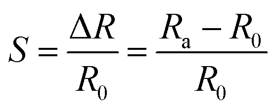 | (1) |
 | ||
| Fig. 1 (a) Schematic illustrations of the synthetic process of MoS2 chemiresistors with active channels fabricated with different CVD methods. (b) Photograph and optical microscope images of the obtained chemiresistors. (c) Resistance changes of the synthesized MoS2 films with distinct layer alignments upon gas adsorption. (d) Response upon exposure to NO2 of varied concentrations.49 Adapted with permission from ref. 49. Copyright 2015 American Chemical Society. | ||
2.2 Field-effect transistors (FETs)
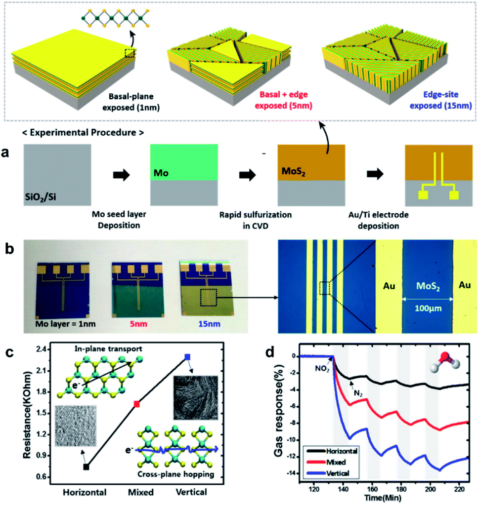
The FET is another widely exploited gas sensing configuration owing to its ease of fabrication, sensitive response, and feasible miniaturization. Typically, FETs consist of a semiconductor as the conducting channel connected by the source and drain electrodes, with the entire structure placed on the top of an insulating layer as gate dielectric, and the conductance of the semiconductor material can be regulated by varying the bias voltage of the gate electrode on the other side of the insulator. The gas sensing response of a FET sensor is determined by calculating the difference between source–drain current and that corresponding to the target analyte under a constant bias voltage. Since most FET gas sensors function in their linear regions, they can be chosen to increase the sensitivity by regulating the gate bias to modulate the charge carrier ability under the same gaseous conditions. To be specific, Fig. 2a and b depict the structure of a FET gas sensor based on MoS2. This sensor exhibits a decreased source–drain current upon exposure to NO2 at concentrations varying from 20 ppb to 400 ppb, while producing an increased current upon exposure to NH3 at concentrations from 1 ppm to 500 ppm at the same gate bias voltage (Fig. 2c and d).50 This observation can be interpreted as the change of the electronic structure of the channel material due to the charge transport between the sensing component and adsorbed analytes. In the case of NH3, since NH3 is a kind of reducing gas, once its molecules come into contact with the device channel materials, electrons would be donated to the n-type MoS2, increasing the electron density and thus the conductance of the channel layer. As a result, the sensing gas composition has a decisive influence on the anticipated response of FET devices.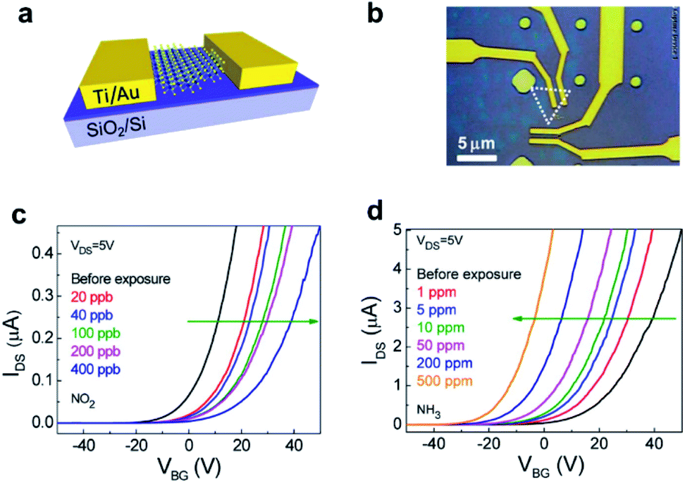 | ||
| Fig. 2 (a) Schematic illustration of the MoS2 FET (back-gate) as a gas sensor. (b) Optical image of two separate devices. (c and d) Transfer characteristics of the MoS2 FET upon exposure to NO2 and NH3 of varied concentrations, respectively.50 Adapted with permission from ref. 50. Copyright 2014 American Chemical Society. | ||
2.3 Diodes
In addition, diodes are effectively utilized for hazardous gas detection because of their high sensitivity and low power consumption. The p–n junction diode and the Schottky diode are two common types of diodes serving as gas sensors. Specifically, a p–n junction diode is built by connecting a p-type semiconductor and an n-type semiconductor together, while a Schottky diode is formed by establishing the junction of a semiconductor with a metal. Fig. 3a presents the structural model and the corresponding optical image of the MoS2 p–n junction gas sensor. The electronic structure of the interfacial barrier (i.e., p–n junction region) would change according to the charge transfer between sensing materials and target analytes when gas molecules are adsorbed onto the surface from either side of the junction. The charge transfer would then influence the current flow traits across a rectifying junction. In the case of exposure to NO2, a well-known electron acceptor, the density of holes would increase in the p-type MoS2 region, while that of electrons decreases in the n-type MoS2 region. In the end, the p–n junction barrier height rises drastically, thus increasing the resistance of the tested device. As shown in Fig. 3b, the p–n junction gas sensor exhibited an enhanced response to NO2 with increasing concentrations.42 This particular device has a detection limit reaching the 0.1 ppm level. Similarly, the Fermi level of sensing semiconductors and the SBH of Schottky diodes at the interfacial junctions can be modulated by the adsorbed analyte molecules on the surface of the gas sensors. Fig. 3c displays the schematic illustration and the optical image of a graphene chemiresistor together with a graphene/Si Schottky device on the same substrate.51 The response upon exposure to reducing gas NH3 for 5 min is presented in Fig. 3d, at concentrations from 10 to 550 ppm. The conductivity declines with increasing concentrations because more electrons get transferred to graphene, depleting more holes in the channel materials under a reverse bias. In this way, a higher gas detection sensitivity can be obtained accordingly. | ||
| Fig. 3 (a) Structural model and optical image of the MoS2 p–n junction gas sensor device. (b) Sensing transients of the sensing response to varied concentrations of NO2. Inset shows the response–recovery curve under low concentration exposure.42 Reproduced from ref. 42. Copyright 2020, John Wiley & Sons, Inc. (c) Schematic and biasing scheme of the graphene chemiresistor and the graphene/Si Schottky diode constructed on the same silica wafer, respectively. (d) Conductivity change over time at different concentrations of NH3 from 550 ppm to 10 ppm, at a reverse bias of −3 V.51 Reproduced from ref. 51. Copyright 2014 John Wiley & Sons, Inc. | ||
2.4 Conductometric sensors
Conductometric gas sensing devices are another popular class of chemical sensing devices. They share many merits of chemiresistors such as the flexibility in fabrication, the simplicity of operation, and the diversity of different detectable gases. It is typical of conductometric semiconducting gas sensors that the interactions between sensing materials and analyte molecules are reversible. For instance, as demonstrated in Fig. 4a and b, the schematic and the optical image show a typical conductometric gas sensor made from a MoS2 monolayer. This sensor exhibits excellent sensitivity and selectivity towards a series of volatile organic compound (VOC) analytes and supports effective transduction of perturbations arising from physisorption events of gaseous molecules into the conductance of the material channel.52 Particularly, the response and sensitivity of the MoS2 monolayer upon a pulse exposure sequence of acetone, a highly polar molecule, is shown in Fig. 4c. The corresponding conductivity increases upon exposure as the concentration of acetone rises from 0.02% P0 (50 ppm) to 2% P0 (5000 ppm). Here, the analyte concentration is monitored as a percent of its equilibrium vapor pressure measured at 20 °C, P0. The exposure pulse sequence is considered the main reason for the incremental variation in conductivity as the amplitude of ΔG/G0 is comparable at a certain concentration. Furthermore, the background shows a positive slope over the total duration upon exposure. Combined with other studies, it is revealed that this sensor gives a highly selective response to electron-donating gas analytes and little response to electron-accepting gas molecules, being in good consistency with the weak n-type features of the MoS2 monolayer.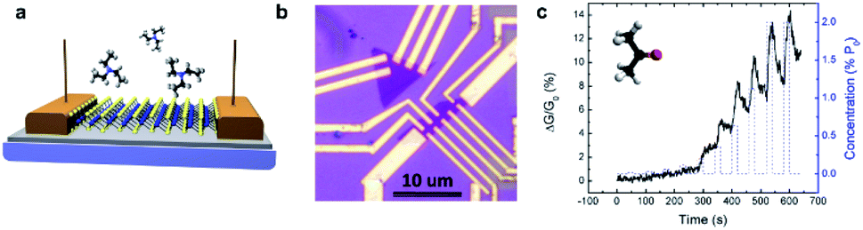 | ||
| Fig. 4 (a) Schematic illustration and (b) optical image of the MoS2 monolayer device. (c) Response of gas sensors to the exposure of acetone. Conductivity change of the MoS2 sensor upon exposure to a sequence of pulses of acetone concentration from 0.02% P0 (50 ppm) to 2% P0 (5000 ppm, black line). Dashed blue line: pulse interval (20 s on/40 s off) and the corresponding concentrations.52 Adapted with permission from ref. 52. Copyright 2013 American Chemical Society. | ||
3. Performance parameters of gas sensors
In principle, the performance of a gas sensor can be evaluated using several critical key parameters including response, sensitivity, selectivity, response time, recovery time, stability, etc.Fig. 5a shows the schematic illustration of the selected performance parameters in a common gas sensor continuously exposed to incremental concentrations of analytes.8 The response (S) of a gas sensor is calculated based on the type of output data. Similar to the definition of the response of a chemiresistor (eqn (1)), the response of a conductometric sensor is defined as the relative variation in its conductivity: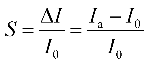 | (2) |
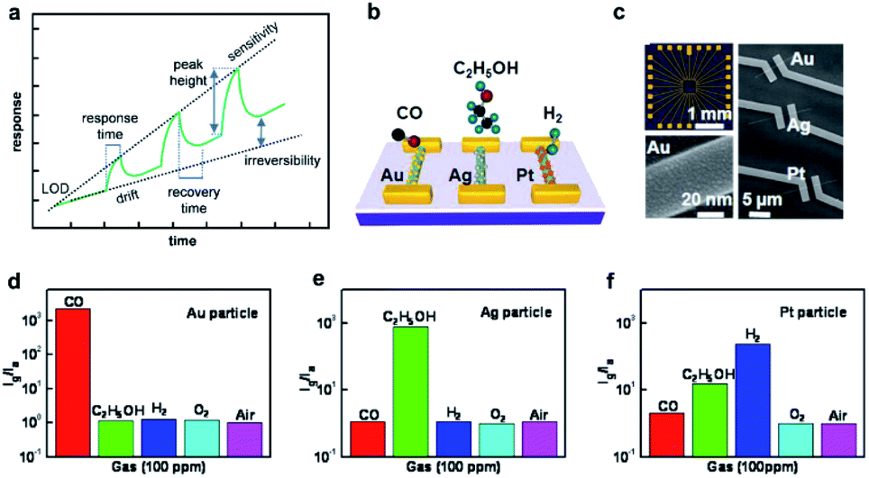 | ||
| Fig. 5 (a) Schematic illustration of the major performance parameters in a device successively exposed to incremental concentration of gaseous analytes.8 Adapted with permission from ref. 8. Copyright 2019 American Chemical Society. (b) Schematic of hybrid chemical sensors, containing three different Mg-doped In2O3 nanowire FETs, whose surfaces are decorated with Au, Ag, and Pt nanoparticles, respectively. (c) Optical (top left) and scanning electron microscope (right) image of chemical sensor arrays. High magnification scanning electron microscope image (bottom left) of an Au decorated Mg-doped In2O3 NW. The sensitivity of (d) Au-, (e) Ag-, and (f) Pt-decorated nanowire FET sensor arrays upon exposure to different gases at 100 ppm.22 Adapted with permission from ref. 22. Copyright 2013 American Chemical Society. | ||
It is indispensable to take into consideration the selectivity of gas sensors since gas detecting scenarios often involve complex gaseous mixtures. Selectivity is generally denoted as the quality of a gas sensor to distinguish analytically target analytes from other gases in uncertain mixtures with no disturbance of irrelevant gaseous components. It can be obtained by statistically analyzing the output signals of mixtures based on a series of patterns of pure gases. It is essential that the experimental conditions are kept identical to eliminate unnecessary deviations. The selectivity of analytical gas sensors is naturally induced by the existence of recognition elements selectively interacting with analytes of interest and then being transduced into output signals in the form of discernible curves. Techniques including the hybridization of sensing configurations can be employed to facilitate the selectivity of gas sensors. For example, Zou et al. designed a hybrid gas sensing configuration and demonstrated it as an effective platform with high sensitivity and gas specific selectivity. Fig. 5b and c illustrate the gas sensing devices based on Mg-doped In2O3 nanowires decorated with Au, Ag, and Pt metal nanoparticles, separately. These devices are able to differentiate unequivocally three reducing gaseous molecules (CO, H2, and C2H5OH), respectively, under complicated ambient conditions (Fig. 5d to f).22 In particular, the gas sensing device with Au nanoparticle decoration exhibits higher orders of magnitude response towards CO molecules of 100 ppm among gaseous mixtures at room temperature. Besides, the selectivity to target analytes can also be realized and regulated via surface functionalization of sensing materials by virtue of surface chemistries, which can possess a good affinity to specific analytes and thus generate extraordinary responses. For example, metal–organic frameworks (MOFs) can achieve tunable selectivity to VOCs or small gaseous molecules (e.g., NH3) when incorporated with certain metallic nodes.53 In this case, the selectivity can be further enhanced by optimizing the experimental parameters during the MOF synthesis, such as temperature, pressure, and others.
Apart from the selectivity, the LOD refers to the lowest concentration of the analyte of interest that can be effectively distinguished in a gas mixture with reliability and repeatability.54 With respect to the determination of the LOD, the calibration curve is firstly obtained by collecting the output signal of the device under a certain concentration of the target analyte. Then, numerous analytical methods are employed to deduce the final LOD from the effectively recorded analytical signals, usually requiring a signal-to-noise ratio greater than 3.54 Since the LOD is dominated by the sensitivity of a gas sensor, it could be improved via various techniques, such as enhancing the material−analyte binding interactions, increasing the available surface area, functionalizing the sensing materials, and amplifying the output signals.55 This way, covered chemically functional groups on low-dimensional materials would facilitate strong interactions with target gas molecules to yield the sensitive response of the device. In turn, the intrinsic conductivity of channel materials and high quality of their interfaces would bring about a small noise level in the collected signal for gas detection. Both characteristics together can make gas sensors exhibit low LODs.56
Furthermore, the response and recovery time are primary parameters to assess the detection performance of sensing materials in gas sensors. The response time refers to the time taken by the output curve to reach 90% of the final increased value from the benchmark, while the recovery time is considered as the time required for the output signal to restore to its initial value under no analyte exposure. With respect to the reversibility of gas sensors, it is so crucial for gas sensors to exhibit full recovery behavior that gas sensors can function for sustaining the analyte detection. Factors, such as sensor configuration, recognition elements, and measurement techniques, play significant roles in the determination of the response time of gas sensors. Technically, sensing materials with low dimensionalities can benefit the diffusion rate of gas analytes across the surface binding sites, thus inducing a fast electrically transduced response.
In addition, stability describes the performance of a gas sensor to generate identical response signals during the same interval of the alternant charge and discharge of gas analytes. The stability of gas sensors is usually assessed by quantitatively comparing the sensing output of a new device and that of an aged one. Gas sensors with excellent stability are suitable for continuous and long-term operation for hazardous gas monitoring. That is, the sensing device should remain reliable over its entire lifespan in terms of various realistic application scenarios. Importantly, the lifetime of gas sensors mainly relies on the stability of the employed sensing components themselves when exposed to an environment of complex physical and chemical factors.8,40 Nevertheless, the focus of specific performance parameters for a gas sensor is highly dependent on its actual application scenario. For example, sensors with great selectivity and sensitivity to VOCs (e.g., acetone and ethanol) can be used for the early diagnosis of diseases and environmental monitoring. There is a recent development by Kim et al. utilizing metallic MXenes as the active sensing materials, in which the fabricated sensors show extraordinarily high sensitivity (even reaching the ppb level) and selectivity to VOCs exhibiting an ultrahigh signal-to-noise ratio (Fig. 6).17 All this suggests the potential of functionalized metallic sensing/transport channels for greatly sensitive gas monitoring.
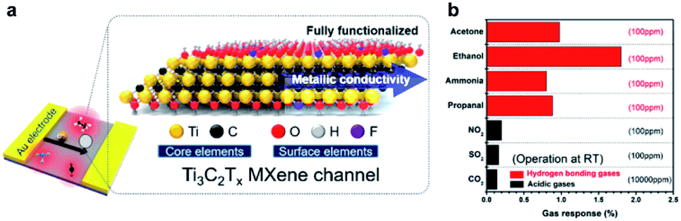 | ||
Fig. 6 (a) Schematic illustration of the Ti3C2Tx gas sensor and its atomic structure. (b) Maximum resistance variation upon exposure to 100 ppm of gaseous analytes (e.g., acetone, ethanol, ammonia, propanol, NO2, and SO2), and 10![[thin space (1/6-em)]](https://www.rsc.org/images/entities/char_2009.gif) 000 ppm of CO2 at room temperature (25 °C).17 Adapted with permission from ref. 17 Copyright 2018 American Chemical Society. 000 ppm of CO2 at room temperature (25 °C).17 Adapted with permission from ref. 17 Copyright 2018 American Chemical Society. | ||
4. Sensing mechanisms
The concrete sensing mechanisms involved in gas sensors can be interpreted in terms of the sensing materials, analyte interaction steps and subsequent transduction processes.8,9 In the initial stage, molecular analytes tend to diffuse on the surface of the sensing components and then interact with active sites chemically or physically. The interactions can usually alter the chemical or electronic structures of the channels, which are then transduced into electrical signals in the transduction step. Generally, the interactions between the sensing components and target analytes are categorized into two groups on the basis of bonding types between two elements: (a) non-covalent interactions, including van der Waals (vdW) bonding, hydrogen bonding, and ligand binding; (b) covalent bonding as a result of chemical reactions between both components. Empirically, non-covalent interactions can allow the better reversibility of gas sensing behavior, while covalent bonding would benefit the gas sensing performance in selectivity and sensitivity. The interaction type depends on both of the chemical structures of the sensing layers and analytes. As sensing materials with low dimensionality have distinct chemical compositions, morphologies and surface chemistries, the binding sites for interactions on their surfaces almost vary for each type of material. Taking graphene and metal oxides (MOS) as examples, graphene has abundant sp2-hybridized carbon atoms on the surface, which allow the formation of vdW bonds via the interaction with analytes, accompanied by charge transfer.35,48,57,58 On the other hand, MOS as sensing materials always possess oxygen molecules adsorbed on their surface that undergo chemical redox reactions with gas analytes.20,29,45,59,60 Strategies, such as surface functionalization, defect engineering, and doping, can effectively enrich the surface binding sites and enhance the binding affinities of surface atoms, improving the sensing response of gas sensors.26,31,60–62 For example, Kumar et al. realized tunable gas sensors based on graphene by controlling external defects in silica substrates without any negative influence on the intrinsic electrical and structural properties of graphene. In the case of the doping effect, Xu et al. reported that a sulfur-doped SnO2 gas sensor exhibited enhanced selectivity towards NO2 molecules as compared to cross-response to various analytes (e.g., ethanol, acetone, SO2, H2S, HCHO, and xylene) in Fig. 7a, where the exponentially increased sensitivity and selectivity are mainly ascribed to the enhanced adsorption capability and catalytic activity of SnO2 by optimal S doping.60 The response was assessed by measuring the ratio of sensor resistance in target gases (Rg) to that in fresh air (Ra). In another example as depicted in Fig. 7b, the Ti3C2Tx-F sensor displays a sensitive and selective response towards oxygen-based molecules (e.g., ethanol and acetone) owing to the increased surface areas as compared to pristine materials (Ti3C2Tx and Ti3C2Tx-Cl).31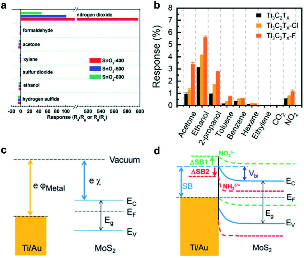 | ||
| Fig. 7 (a) Responses of SnO2-400, SnO2-500, and SnO2-600 to 5 ppm of a series of gases at optimal temperature. The numbers 400, 500, and 600 are the sintering temperatures under an air atmosphere for the synthesis of SnO2 with different S doping concentrations.60 Reproduced from ref. 60. with permission from the Royal Society of Chemistry. (b) Maximum response variation upon exposure to various gases of MXene gas sensors.31 Adapted with permission from ref. 31. Copyright 2020 American Chemical Society. (c) Energy diagram of Ti/Au and MoS2 before coming into contact. (d) Band realignment and energy diagram of metal electrodes Ti/Au and MoS2 after coming into contact and the formation of the Schottky barrier. Each energy band is marked as follows: MoS2 (solid blue), MoS2 exposed to NO2 (dashed green), and MoS2 exposed to NH3 (dashed red). ΔSB1and ΔSB2 are Schottky barrier (SB) changes under NO2 and NH3, respectively.50 Adapted with permission from ref. 50. Copyright 2014 American Chemical Society. | ||
In a typical transduction phase, the induced alterations in the physical or electrical properties of the sensing materials due to the sensing material/analyte interactions are ultimately converted into electrical signals. Most transduction principles could be interpreted and summarized as the several following modes: the regulation of the doping level, the control of the SBH, and the formation of interfacial ionic bilayers. Specifically, a reasonable distance between analytes and sensing materials is important for efficient charge transfer during the process of analyte/sensing material interaction. Considering the relative electronic structures of both components, the charge transfer could result in a p-type or n-type doping effect with analyte gases serving as an electron acceptor or donor, respectively. Since most sensing materials are semiconductors, external doping would lead to the change of the net doping charge density of the sensing materials. In other words, the Fermi level of a pristine material defined during the synthesis is about to shift closer to the valence band or conduction band. As a result, the doping level can drastically influence the density of states (DOS) and thus the conductivity of the channel materials. The site-binding extent on the surface varies at different concentrations of the analyte gases; therefore, the doping level is accordingly regulated by the adsorption density of surface atoms. Due to the feature of abundant binding sites on the surface originating from a high surface area-to-volume ratio, sensing materials with low dimensionalities can sensitively respond to analyte exposure and are especially preferable for gas detection and monitoring.
In most gas sensors, metal electrodes are employed to collect the electrical output signals. Metal–semiconductor junctions are usually formed at the contact between electrodes and sensing materials, where potential barriers would exist when the work functions of these two elements mismatch. In the case of n-type semiconductors, the Schottky barrier height is the difference of work function values of the semiconductor and electrode metal in the electrical contact. For example, Fig. 7c displays the energy band diagram of a Ti/Au metal electrode and n-type MoS2 prior to their physical contact.50 Once the Schottky barrier exists, most charge carriers are not able to surmount the energy barrier and then transport across the interfacial junction, leading to a rectifying behavior. However, the barrier height at the interfacial junction could change when the sensing device is exposed to certain types of analytes. The adsorption of gas molecules on the surface could lead to the alteration of the doping level, the shift of the Fermi level, and the consequent modulation of the barrier height at the junction. When the MoS2 gas sensor configured with Au electrodes is exposed to ammonia, it undergoes n-type doping, exhibiting a decreased SBH. In contrast, it would result in an elevated SBH when operated in NO2, which functions as a p-type dopant (Fig. 7d).50 The characteristic modulation of the barrier height to influence the charge transport in electrically transduced devices is also introduced into the design and production of high-performance gas sensors in the form of Schottky diodes.
At the same time, the interactions between analytes and sensing components also tend to bring about the ionization of adsorbed analyte molecules, forming a dipole layer at the interface. In this way, the charge states at the junction could regulate the barrier height. The formed ionized layer is anticipated to induce the redistribution of charges in the depletion region and reshape the band bending at the junction interface. This phenomenon is more familiar in n-type metal-oxide semiconductors. O2 molecules are usually pre-adsorbed on the semiconductor surface under ambient conditions in the form of negative ions such as O2−, O−, and O2−. These oxygen species induce a space-charge region on the surface of the sensing material, which shall create a potential barrier among the adjacent grains, hindering the transport of charge carriers. When operated in reducing gases, the negatively charged oxygen ions would react with the analytes, leading to the transfer of trapped electrons into the MOS. Thus, the potential barrier among the grains is diminished, consequently increasing the conductance of the channel material. It is more common to experience such a pronounced phenomenon in sensing systems where the grain size of the sensing material is usually closer to or smaller than the thickness of the depletion layer.
5. Low-dimensional materials for gas sensing
5.1 Metal oxides
Metal oxides (MOS) are one of the most investigated materials for gas detecting applications. NiO, SnO2, ZnO etc. configured in distinct nanostructures have been integrated into gas sensors for sensitive and even selective detection of analytes of interest at elevated temperatures. High temperatures (>250 °C) are conducive to the conductivity of MOS by increasing the charge carrier concentration. According to the conduction type, MOS exhibit distinct sensing behaviours towards the same gas analyte. Upon exposure to oxidizing gases (e.g., NO2, CO2, O3, etc.), these gas species would serve as acceptors, leading to a conductivity decrease for n-type MOS and an increase for p-type MOS. In contrast, reducing gases (e.g., NH3, CO, H2, HCHO, etc.) acting as donors usually give rise to a conductance increase for n-type MOS and a decline for p-type MOS. The sensing mechanism of MOS is primarily dominated by pre-adsorbed oxygen ions under ambient conditions, which is interpreted as the ionosorption model. This model includes gas adoption, ionization, and redox reactions, which explains the space-charge effect or the alterations of potential barriers between grains in the material surface. Explicitly, the negatively charged oxygen species on the surface is formed via the following reactions of the exchange electrons:| O2(adsorbed) + e− ↔ O2− (<100 °C) | (3) |
| O2− + e− ↔ 2O− (100−300 °C) | (4) |
| O− + e− ↔ O2− (>300 °C) | (5) |
In this way, the analyses of the depletion layers in MOS′ surface or potential barriers at grain boundaries usually apply to n-type materials, given that there are not any potential barriers existing at grain boundaries. Due to the electron withdrawal effect contributed by the adsorbed oxygen anions on the surface, holes are accumulated in the layer adjacent to the p-type metal oxides' surface, where the hole-accumulation layer can constitute the carrier transport channel. Thus, the thickness of the depletion layer (L) here can be determined according to the Debye length (LD) of the material as the following:
| L = LD(2 eVs/kT)1/2 | (6) |
| LD = (kTε/q2ND)1/2 | (7) |
Recently, Cho et al. developed highly sensitive gas sensors with low-power consumption, in which porous SnO2 nanotubes (NTs) were synthesized and integrated onto a micro-electromechanical-system (MEMS) platform.45 During the synthetic process, ZnO nanowires (NWs) as template materials were directly synthesized via a localized hydrothermal reaction and then etched to deposit a porous thin film of SnO2 in the liquid phase, generating porous SnO2 NTs. It is desirable to operate these MOS based gas sensors at temperatures at which both chemisorption and physisorption are allowed.65Fig. 8a and b show the resistance variation of ZnO NWs and SnO2 NTs by adjusting the heating power. It can be inferred that the suitable operation powers for the ZnO NWs and SnO2 NTs are found in the range of 3–4 and 4.5–6 mW, respectively. Upon exposure to H2S (i.e., reducing gas) of various concentrations, in Fig. 8c and e, the dynamic response of the two materials shows that the highest sensitivities of the ZnO NWs and SnO2 NTs are heated at the power of 6 and 5 W, respectively (e.g., Ra/Rg = 2.06 at 1 ppm for ZnO NWs; Ra/Rg = 6.16 for SnO2 NTs). These results exhibit the higher sensitivity of SnO2 NTs from 1.3 times (5 ppm and 3 mW) to 7.4 times (20 ppm and 5 mW) those of ZnO NWs and lower power consumption of SnO2 NTs. As depicted in Fig. 8d and f, an overall short response and faster recovery times of SnO2 NTs are observed, confirming the better sensing performance of SnO2 NT sensors.
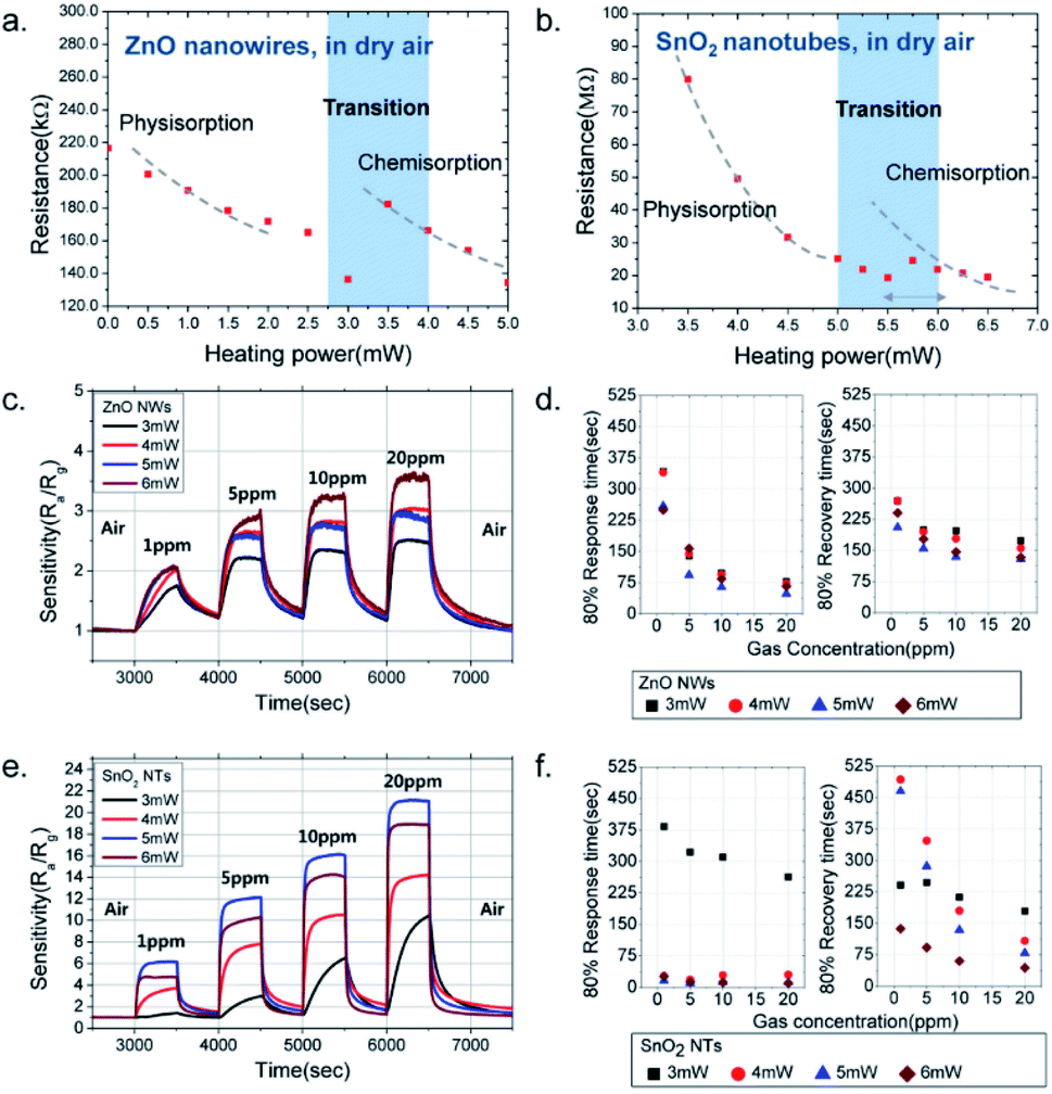 | ||
| Fig. 8 Relationship between the resistance and heating power of the sensors based on (a) ZnO NWs and (b) SnO2 NTs upon exposure to H2S. Dashed lines: physisorption and chemisorption regimes. The sensing performance of H2S: (c and e) sensing responses of ZnO NWs and SnO2 NTs (produced at pH = 4), respectively, at varied heating powers; (d and f) 80% response time and recovery curve of the corresponding materials at gas concentration varied from 1 to 20 ppm.45 Adapted with permission from ref. 45. Copyright 2017 American Chemical Society. | ||
Nevertheless, it still remains challenging for MOS based gas sensors aimed for the selective monitoring of VOCs at room temperature. Xu et al. reported the highly sensitive and selective detection of triethylamine (TEA) at room temperature utilizing SnO2 thin-film sensors.66 It is worth mentioning that defect engineering is introduced into the fabrication of these porous SnO2 films. Oxygen vacancies as defects proved to be significant for room-temperature sensing performances. When exposed to analytes, the incremental responses with good reproducibility are shown in Fig. 9a, at concentration from 0.5 ppm to 100 ppm. The sensor response is also compiled in a range of working temperatures from 30 to 220 °C as demonstrated in Fig. 9b. It is pronounced that this gas sensor can effectively function at relatively low temperatures (e.g., its response reaching about 150 at 30 °C). The corresponding LOD is determined to be 110 ppb (Fig. 9c), manifesting the device's capability to sensitively detect TEA. More importantly, the responses to diverse interfering mixtures (e.g., TEA, acetone, methanol, ethanol, N-butanol, formaldehyde, NH3, H2, and NO2) are also carefully studied and presented in Fig. 9d. It is seen that the gas sensor exhibits a highest selectivity to TEA at room temperature. The main reasons for the high selectivity of the SnO2 sensor to TEA can be ascribed to the higher active C–N bonds, the strong electron-donating ability of ethyl groups, and the higher affinity of N atoms with its lone pair electrons in the TEA molecules.67,68 All these results illustrate the potential of using MOS as active materials for gas detection.
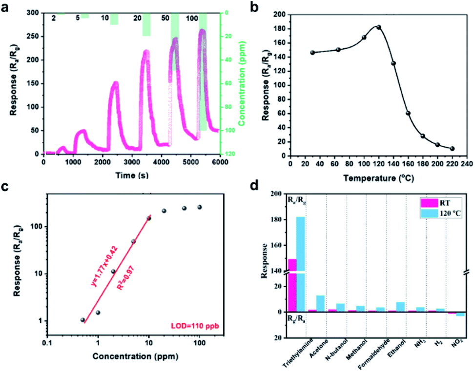 | ||
| Fig. 9 (a) Dynamic response curves of the porous SnO2 film sensor to incremental varying TEA concentrations at room temperature. (b) Response to 0.5–100 ppm of TEA. (c) Response at different operating temperatures of the SnO2 film sensor to 10 ppm of TEA. (d) Histogram responses of the SnO2 film sensor at room temperature and 120 °C.66 Adapted with permission from ref. 66. Copyright 2020 American Chemical Society. | ||
5.2 III–V semiconductors
III–V compound semiconductors, such as AlAs, InAs, InSb, GaAs, InP, InGaAs, etc., are a class of materials composed of elements of columns III and V in the periodic table.69–72 Particularly, electron mobility in certain III–V semiconductors, such as InAs or InGaAs, is more than 10 times higher than that of silicon at a comparable carrier concentration.69 When they are configured into the nanoscale, III–V compound semiconductor NWs are extensively explored as building block materials for electronic devices due to their superb electronic transport characteristics as well as low leakage currents. Importantly, the electron surface accumulation layer is deemed conducive to excellent surface sensitivity to many gas analytes.Based on these unique characteristics of III–V materials, Paul et al. developed a chemiresistive gas sensor based on n-type InSb NWs via a chemical vapor deposition (CVD) growth method, exhibiting a remarkable response in the detection of NO2 down to 1 ppm at room temperature.21 The resistance of the InSb sensor is found to rise with the concentration of NO2, since the analyte served as a great electron acceptor, reducing the charge density in NWs via the charge transfer from InSb NWs to NO2 molecules. Similar results were also observed in gas sensors based on InAs NWs.73,74 Notably, the sensing ability of InSb NW sensors could be extended to some other reducing or oxidizing gas analytes. As illustrated in Fig. 10a, Du et al. reported the gas-exposure response of InAs NW-FETs to various gaseous molecules or chemical vapors (e.g., ethanol, acetone, IPA, and water) and explored the corresponding sensing mechanism of the horizontal NW device structure.73 The results show that the adsorption of analyte molecules on the surface of InAs NWs would induce charge transfer and then improve the carrier mobility of the NW remarkably. The response to analytes is compiled in Fig. 10b, in which the conductance gradually increases as the analytes are introduced owing to the electron transfer from adsorbed analytes to n-type InAs NWs. Once the gases are removed, the recovery process starts with the falling of the conductance. By studying the gate voltage (Vg) dependence of the InAs conductance to quantitatively understand the extent to which charge transfer would occur after the gas molecules' adsorption, it is found that the chemisorption and charge transfer at the surface can reduce scattering and hence improves the charge carrier mobility. Offermans et al. demonstrated the sensitive detection of NO2 with concentrations below 100 ppb at room temperature with a sensing platform based on vertical InAs NWs as illustrated in Fig. 10c. The vertically aligned NW arrays are considered an enhanced gas sensing platform because of the easier access and the larger contact surface area with gas molecules; however, the corresponding device fabrication will be slightly complicated as compared to the horizontal counterpart. In this case, NO2 exposure gives rise to a decrease of both the charge carrier density and the mobility.74 During NO2 exposure, the response (I − ΔI/I0; I, I0 and ΔI are the output current with gas sensing, initial output current and changes of the output current, respectively) increases during NO2 exposure, recovering after nitrogen flushing as shown in Fig. 10d. The decline in current in gas exposure is believed to be due to the electron doping effect of NO2 molecules, which would decrease the electron density in the surface electron accumulation layer of the InAs NW arrays.
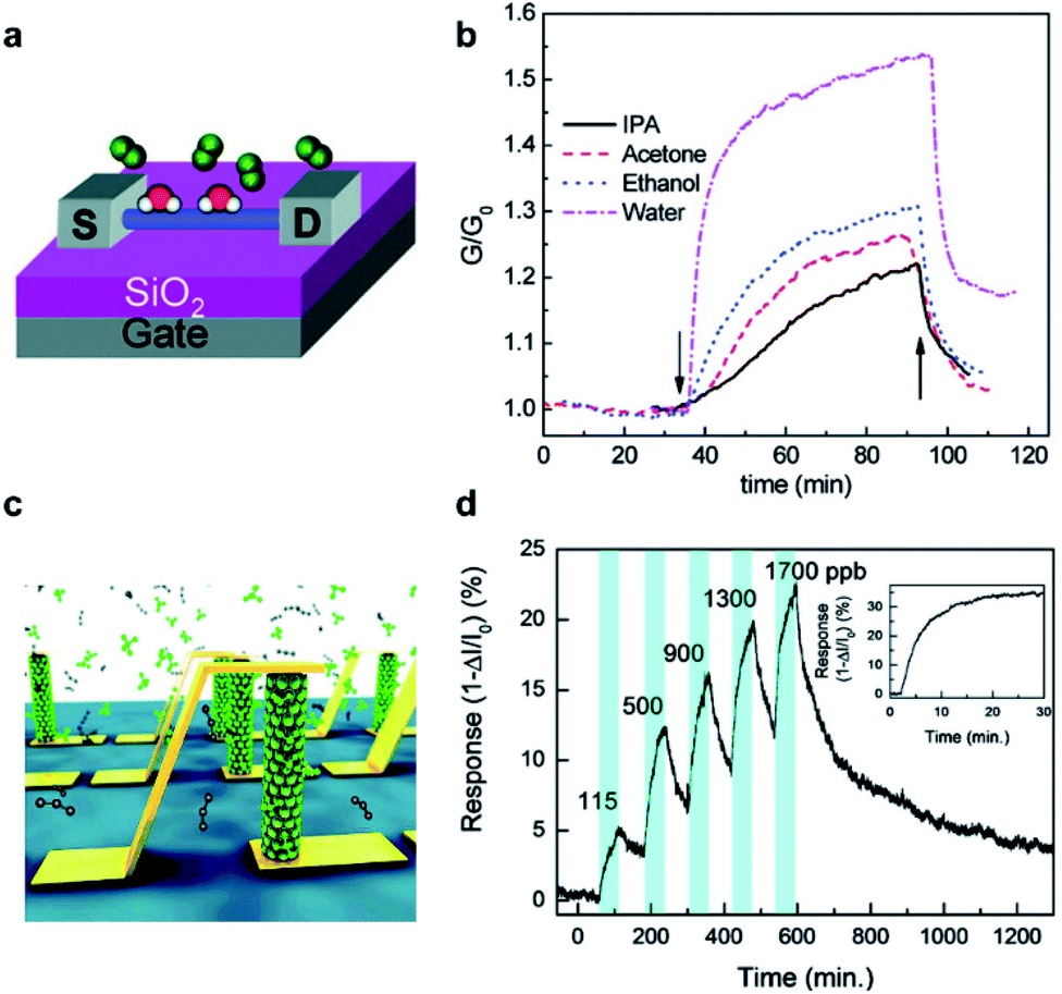 | ||
| Fig. 10 (a) Schematic of InAs nanowire device. (b) Response of the InAs nanowire FET upon exposure to analytes.73 Adapted with permission from ref. 73. Copyright 2009 American Chemical Society. (c) Illustration of the selective adsorption of gas molecules on a vertical nanowire surface. (d) Response of an InAs nanowire array to the varying concentrations of NO2 in a N2 environment. Inset: saturated response to 9 ppm NO2/N2.74 Adapted with permission from ref. 74. Copyright 2010 American Chemical Society. | ||
5.3 Graphene and graphene oxide
Graphene is an atomic-thin layer of sp2-hybridized covalently bound carbon atoms. It possesses a large surface-area-to-volume ratio, allowing for the large site-binding capacity of gas analytes and strong surface activities.58 Furthermore, graphene exhibits an extremely high carrier mobility reaching 105 cm2 V−1 s−1 and a high carrier density of up to 103 cm−2 at room temperature.37,75 These remarkable electronic properties make graphene extremely attractive for the manufacture of excellent analytical electronics.76 The surface of graphene can be conducive to interactions with analytes via electron transfer, covalent bonding, etc.77 That is, the small chemical or physical stimuli arising from the analyte molecule adsorption on graphene's surface could lead to the perturbation of its electronic properties due to its low electrical noise.78 Thus, graphene, graphene oxide (GO), reduced graphene oxide (rGO), and their functionalized materials have been intensively exploited for gas-sensing applications.35,48,57,58,77In general, graphene monolayers were first prepared and transferred onto the surface of SiO2, followed by the fabrication of devices with Au electrodes. These devices were aimed to investigate graphene's electronic properties under the perturbation by the adsorption of gas molecules (e.g., NH3, NO2, H2O, and CO). It is found that its charge carrier concentration would increase linearly with the rise of the concentration of NO2.57 Also, the reverse response upon exposure to electron donor molecules (e.g., NH3) against electron-acceptor gases (e.g., NO2) exists.57 The excellent performance of graphene when exposed to surface adsorbates is mainly ascribed to the maximum interactions with adsorbates, its metallic conductivity, its low levels of excess noise (i.e., 1/f noise) because of its high crystallinity, and the ohmic contact of the device. Pristine graphene can detect analytes of low concentrations, which was confirmed by the ppb level detection of various gas analytes in the literature (e.g., NO2, NH3, N2O, O2, SO2, CO2, etc.).36
In fact, the gas sensitivity of intrinsic graphene can be improved by introducing defects or doping with impurities. For instance, Zhang et al. found that the interactions between analyte molecules and pristine graphene are rather worse than those of the defective or doped counterparts.61 In order to verify the influence of these defects in graphene, Johnson et al. also experimentally compared the sensing responses of FET devices after mechanical exfoliation, those of the devices after contact fabrication via electron beam lithography (EBL) and electrode metal deposition, and those of the devices after a cleaning process.33 They found that the contaminated layer could enhance the carrier scattering and also serve as an absorbent for the preconcentration of analytes on the graphene surface, thus improving the sensor response.
On the other hand, GO and rGO have also been proved to be promising sensing materials. Specifically, Lee et al. reported gas sensor arrays based on hydrophilic GO and hydrophobic rGO.34 This sensor array demonstrated a high selectivity and high sensitivity to VOCs particularly in harsh environments, such as high humidity and strongly acidic or basic conditions. It is also noted that the GO and rGO sensor arrays can effectively distinguish tetrahydrofuran from dichloromethane, respectively, even at relatively low concentrations, where this device performance cannot be easily achieved by other active sensing materials. It is believed that the GO surface has abundant oxygen functional groups and a large surface area. Therefore, GO possesses high gas-sensing capabilities for the strong adsorption of analyte molecules on its surface.
5.4 Transition metal dichalcogenides
Transition metal dichalcogenides (TMDCs) are a group of inorganic materials denoted as MX2, where M and X refer to a transition metal atom (e.g., W, M, etc.) and a chalcogen atom (e.g., S, Se, and Te), respectively.41,79,80 Single-layered TMDs have been highly attractive for a wide range of applications, such as catalysis, electronics, photonics, chemical sensors, and so on, due to their novel chemical, physical, and electronic properties. In terms of conductivity, bulk TMDCs includes insulators (e.g., HfS2), semiconductors (e.g., MoS2), semimetals (e.g., WTe2), and metals (e.g., NbS2).8,81 The electronic properties of TMDC thin-layered structures are distinct from their bulk counterparts because of the confinement effects and the interruption of the interlayer coupling.82For gas sensing applications, 2D TMDs have also been one of the most attractive materials because of their remarkable properties, which include their tunable band gap, high surface-area-to-volume ratio, and reliable operation at room temperature,30,41 being similar to the popular investigation of graphene as a gas sensor.35,58 Li et al. first demonstrated a MoS2 sensor toward gas sensing by integrating mechanically exfoliated MoS2 of few layers into a FET device. It was found that the few-layered MoS2 exhibited n-type transport behavior upon exposure to NO, where its detection limit could be down to 0.8 ppm (Fig. 11a). In addition, the percentage change of output current of the 2 L MoS2 FET exhibits an obvious dependence of NO concentration (Fig. 11b). Although the current response is relatively high, the detection limit is suppressed by the low signal-to-noise ratio. The authors also found that single-layered MoS2 exhibited thickness-dependent sensitivity in the layered MoS2 gas sensor. That is, the sensing performance of the MoS2 FET devices could be enhanced with the increase of the number of MoS2 layers.83 Similarly, Late and co-workers also demonstrated thickness-dependent behavior of the sensitivity regarding thin-layered MoS2.84 They discovered that 5-layered MoS2 showed better gas sensing performance as compared to 2-layer MoS2 upon exposure to NO2 (100 ppm) or NH3 (100 ppm) as shown in Fig. 11c and d. It is considered that the charge transfer is the primary sensing mechanism dominating gas sensing response of most TMD based sensors since the lateral surface of 2D TMDs contains no dangling bonds, which allow for the physisorption of gases.
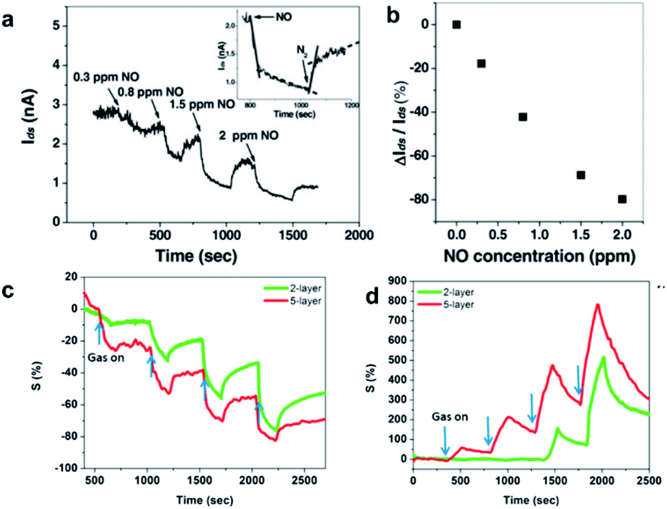 | ||
| Fig. 11 (a) Real-time response upon exposure of the 2 L MoS2 FET to NO with an increased concentration. Inset: typical adsorption and desorption process of NO molecules on the MoS2 FET. (b) Plot of the percentage change of output current versus NO concentration.83 Reproduced from ref. 83. Copyright 2012 John Wiley & Sons, Inc. Comparative 2 L and 5 L MoS2 sensing performances in (c) NH3 and (d) NO2 of 100, 200, 500, and 1000 ppm, respectively.84 Adapted with permission from ref. 84. Copyright 2013 American Chemical Society. | ||
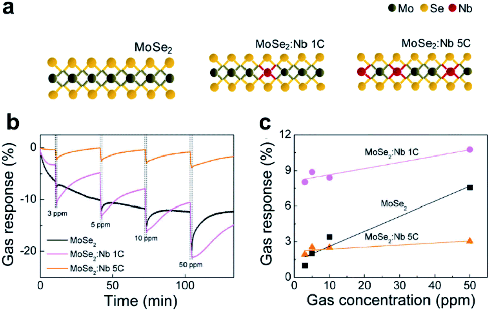
As predicted, regulating the electronic properties of TMDCs via doping has also been illustrated as another effective way to improve the sensitivity to different gaseous analytes. For instance, Zhang et al. investigated the adsorption behavior of Rh-doped MoSe2 at room temperature using theoretical calculations of the density functional theory (DFT) method.85 They found that the Rh–MoSe2 monolayer has a superior response upon exposure to H2 and C2H2 molecules with a sensitivity of around 98.56% and 99.63%, respectively. Meanwhile, the Rh–MoSe2 monolayer was proved to have a good desorption characteristics for H2 molecules. In addition, frontier molecular orbital theory was conducted and confirmed the conductivity change in the presence of gaseous molecules due to the charge transfer mechanism. Recently, Choi and co-authors reported the influence of Nb doping of MoSe2 on its gas sensing capability.86 In the synthesis process, the Nb doping concentration of MoSe2 was finely controlled by adjusting the deposition cycles of Nb2O5 as shown in Fig. 12a. The doping of Nb can diminish the existing dangling bonds and vacancies on the MoSe2 surface, conducive to the prolonged sensing stability of the employed material. Fig. 12b and c display the transient response of all devices (i.e., MoSe2, MoSe2:Nb 1C, and MoSe2:Nb 5C based devices) upon exposure to varied NO2 concentrations (i.e., 3, 5, 10, and 50 ppm). The deteriorated response to NO2 at high Nb doping concentration is ascribed to the increase in the carrier density of metallic NbSe2 regions, which exhibit no response to gas molecules. A low Nb-doped MoSe2 gas sensor showed an improved durability and better response to NO2 molecules, owing to the small crystal grains and stabilized grain boundaries.
 | ||
| Fig. 12 (a) Schematic atomic structures of MoSe2 (left), MoSe2:Nb 1C (center), and MoSe2:Nb 5C (right). (b) Transient gas response of MoSe2 and doped MoSe2 gas sensors to NO2 concentrations varied from 3 to 50 ppm. (c) Comparison of the gas responses of the three devices versus NO2 gas concentration.86 Adapted with permission from ref. 86. Copyright 2017 American Chemical Society. | ||
5.5 Other materials
Other materials, such as black phosphorus (BP), MXenes, and metal–organic frameworks (MOF), are also attracting substantial attention for applications in gas detection and monitoring due to their outstanding structural, chemical, physical, or/and electronic properties. Among them, atomically thin 2D BP possesses good carrier mobility and structural properties. In particular, BP has a high chemical adsorption energy and its puckered surface structure endows it with a great abundance of available binding sites facilitating analyte adsorption.27,87 In 2014, Chen et al. predicated that BP could function as a superior gas detecting material to other 2D materials (e.g., graphene, MoS2, etc.). According to their results, the superior charge transfer is the dominant mechanism supporting the strong adsorption of gaseous molecules on the BP surface.27 Later, this prediction was verified experimentally. Zhou et al. realized the sensitive detection of NO2 gas down to 5 ppb in Ar using a BP-FET sensor (Fig. 13a).87 Additionally, it is shown that the conductance change increases monotonically as the gas concentration rises from 5 to 40 ppb (Fig. 13b). Also, Cui et al. reported 2D layered BP FET sensor devices fabricated via mechanical exfoliation and employed the device for the sensitive monitoring of NO2 at various concentrations from 20 to 1000 ppb (Fig. 13c).32 Notably, the thickness dependency of BP sensitivity towards NO2 gas showed an optimum thickness of 4.8 nm (Fig. 13d).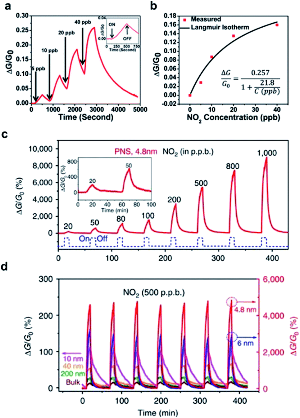 | ||
| Fig. 13 (a) Response curve of a multilayer BP sensor to NO2 concentrations (5–40 ppb). Inset: response to 5 ppb NO2 exposure. (b) The plot of ΔG/G0versus NO2 concentration.87 Adapted with permission from ref. 87. Copyright 2015 American Chemical Society. (c) The plot of ΔG/G0versus time with varied NO2 concentration. (d) Determination of the optimal response with different BP layer thicknesses.32 Adapted with permission from ref. 32. Copyright 2015 Springer Nature. | ||
However, the major challenge in utilizing BP layers for sensing applications lies in its poor stability towards light and oxygen, where BP decomposes into phosphoric acid species in the presence of moisture.87 As compared to MXenes, MXenes are an emerging group of 2D transition metal carbides or nitrides synthesized by selectively etching the element from Mn+1AXn phases, where M, A, and X denote a transition metal, a main group element (e.g., group III A and IV A), and C and/or N, respectively.88 The chemically exfoliated MXenes are typically terminated with functional groups (e.g., –O, –F, and –OH), which are generated in the chemical etching process. These terminal groups contribute to both the charge transfer process and interactions with diverse analytes.8 Besides, the terminal groups such as O− can also alter the electronic structures of MXenes, leading to the conductivity transition from metallic to semiconducting.89
Actually, with recent advances, MXenes have been experimentally demonstrated as promising functional materials for various applications in energy storage and conversion, catalysis, gas sensing, etc.39,48 Both high conductivity and abundant functional groups on the surface together endow MXenes with potential for chemical sensor applications with a high signal-to-noise ratio due to their effective and strong interactions with gas analytes and a low signal noise. For instance, Lee et al. reported a Ti3C2Tx based sensor that possessed a p-type sensing behavior towards multiple gas analytes (e.g., NH3, ethanol, methanol, and acetone).56 It showed the highest sensitivity upon exposure to NH3 molecules of 100 ppm at room temperature. The high sensing quality of this device could be ascribed to the strong adsorption of NH3 onto the surface of MXenes via the molecular analyte interactions with surface functional groups as well as defects.
In addition, metal–organic frameworks (MOFs) are a class of crystalline and porous hybrid materials, which are synthesized via molecular self-assembly of inorganic metallic nodes with the assistance of ditopic or polytopic organic ligands (e.g., carboxylate, thiol, hydroxyl, and amino).90 Among all MOFs, inherently conductive 2D MOFs can be chosen for application in electronic devices such as gas sensing and vapor capture.8,18,48 Conductive 2D MOFs have been produced from redox active planar aromatic ligands with ortho-disubstituted hetero-donor atoms (i.e., O and S). These atoms are coordinated to transition metal ions exhibiting square planar coordination characteristics. As an emerging 2D nanosheet structure, conductive 2D MOFs have attracted enormous attention for utilization in gas sensors due to their exceptionally large surface area, high porosity, and metallic conductivity. Dincă et al. fabricated a cross-reactive sensor array based on 2D MOFs. The gas sensor was capable of distinguishing several classes of VOCs of distinct functional groups (e.g., alcohols, ethers, ketones, etc.). Here, three separate MOFs, namely Ni3HITP2, Cu3HITP2, and Cu3HHTP2, were integrated into chemiresistive sensors via drop-casting. The chemiresistive responses of the three devices upon exposure to different VOC vapors of 200 ppm is presented in Fig. 14a. It is observed that polar VOCs generated a higher response, while the device showed no appreciable signal in aliphatic hydrocarbons. After performing the principal component analysis (PCA) method, it is illustrated that the chemiresistive responses can distinguish among five groups of VOCs with up to 90% precision.91 Additionally, an improvement in the gas sensing quality of 2D conductive MOFs was also recently reported by Xu and co-workers. The authors investigated and developed a layer-by-layer epitaxial growth method to fabricate thin films of Cu3HHTP2 MOFs into a chemiresistive sensor. The response and recovery processes were up to 54% faster than those of the bulk powder counterparts (Fig. 14b), which could be attributed to enhanced interactions of gaseous analytes at the binding sites in the MOF material with a high diffusion rate. Moreover, the fabricated gas sensors exhibited good detection limits down to 0.5 ppm towards NH3 exposure and little interference from other reducing gas analytes (including different VOCs, H2, and CO. Fig. 14c).92
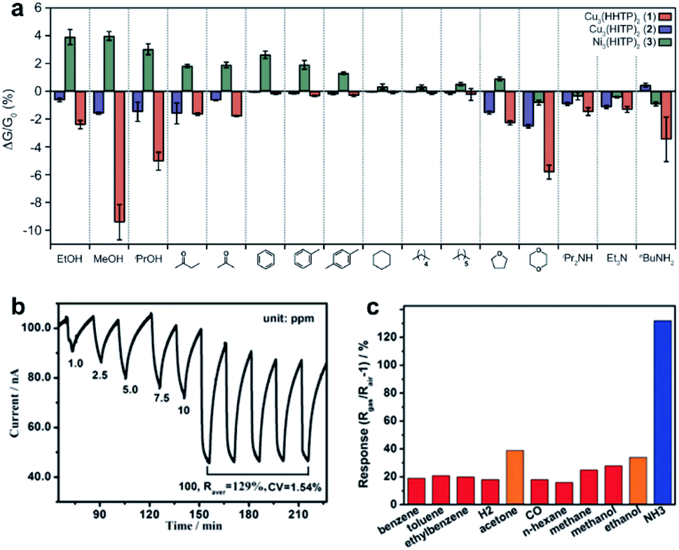 | ||
| Fig. 14 (a) Sensing responses of the MOF array sensor to different VOCs of 200 ppm.91 Adapted with permission from ref. 91. Copyright 2015 American Chemical Society. (b) The response–recovery curve toward NH3 at different concentrations. (c) Comparison of the response to NH3 over other VOCs and gas analytes.92 Reproduced from ref. 92. Copyright 2017 John Wiley & Sons, Inc. | ||
5.6 Hybrid material systems
Although excellent sensing qualities of various single material-based gas sensors have been demonstrated, the sensitivity, selectivity, LOD, and stability of single material-based gas sensors may still suffer from severe interference from other molecules, surface oxidation, moisture absorption, etc. Given that the interaction between analytes and sensing materials is a prerequisite for the operation of any gas sensors, this issue can be resolved by constructing hybrid composite materials at the nanoscale other than doping or defect processing. Typical methods include the incorporation of metal nanoparticles and the functionalization with other sensing constituents onto the active sensing materials. This way, these active sites exhibiting specific and strong binding affinities can be effectively introduced into gas sensing systems. In fact, the gas sensors using hybrid materials as sensitive transducers can achieve two main pronounced advantages in comparison to those of the single constituent. More importantly, diverse combinations of hybrid materials are available for the exploration of better sensing behaviors. In this case, multiple sensing mechanisms can be involved to modulate and substantially enhance the sensing performance via catalytic effect, charge transfer, and construction of heterojunctions.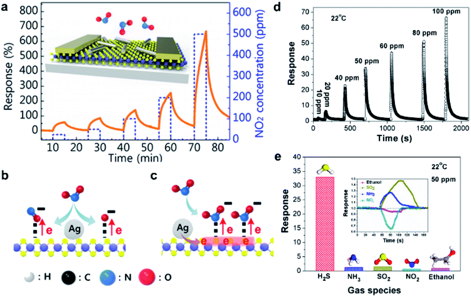 | ||
| Fig. 15 (a) Response of the Ag NW/WS2 gas sensors upon NO2 exposure (25, 50, 100, 200, and 500 ppm). (b) Schematic of the adsorption of NO2 molecules on the WS2 surface catalytically enhanced by Ag NWs. (c) Schematic of electron transfer from the Ag NWs and increase of the electron concentration of WS2.94 Adapted with permission from ref. 94. Copyright 2016 American Chemical Society. (d) Response curves toward different concentrations of H2S. (e) Selectivity of the optimal gas sensor employing SnO2/rGO nanocomposites. Inset: response curves upon exposure to the corresponding analytes.95 Adapted with permission from ref. 95. Copyright 2016 American Chemical Society. | ||
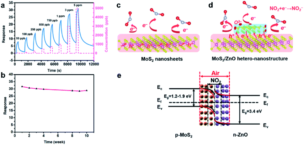 | ||
| Fig. 16 (a) Dynamic response curves of the MoS2/ZnO gas sensor towards different NO2 concentrations. (b) Stability of the MoS2/ZnO gas sensor towards 5 ppm NO2 for 10 weeks. Schematic illustration of the sensing mechanisms of (c) pure MoS2 nanosheets, (d) MoS2/ZnO heterostructures to NO2 molecules and (e) energy band structure of the MoS2/ZnO heterostructures in air and NO2 atmospheres.97 Adapted with permission from ref. 97. Copyright 2018 American Chemical Society. | ||
6. Conclusions and outlook
In this review, we describe various hazardous gas sensing applications based on different low-dimensional materials and hybrid material combinations. Low-dimensional materials, such as MOS, TMDs, MXenes, BP, MOFs, etc., tend to possess unique structural, chemical, physical, and electronic properties, making them the most attractive sensing elements for gas sensors. We also discuss the major components, the common configurations of gas sensing platforms and fundamental transduction principles that output electrical signals of the gas sensing response. Then, we outline the major performance parameters of gas sensors and subsequently the main underlying sensing mechanisms governing the gas detection operation process. Notably, we elaborate the compositional and structural characteristics of various low-dimensional materials, including single materials and hybrid systems as well, allowing their fascinating applications in electrically transduced gas sensors. In terms of various concrete cases of specific materials for sensitive gas detection, we exemplify the outstanding sensing properties and articulate the underlying mechanisms of the corresponding electrical-transduced gas sensors.Although numerous excellent gas sensing platforms integrated with low-dimensional materials have been realized, there still remain substantial challenges in achieving the sensitive gas-detection regime. An extreme low detection limit of gas sensors is necessary for various hazardous gases. An ultralow detection limit down to the ppb level can alert people to the potential exposure to harmful conditions in advance. Future efforts need to be devoted to the further development of gas sensors exhibiting lower detectivity, higher sensitivity and selectivity towards the gas analytes of interest: (i) for higher sensitivity, strategies including size control, chemical modification, doping, defect generation and control, and functionalization with other materials have proved their great effectiveness in the improvement of gas sensing performance, through which the interactions between analytes and the sensing materials can be enhanced, leading to a more sensitive response to the chemisorption or physisorption of molecular analytes; (ii) for the detection limit, enhancing material–analyte interactions, larger surface areas, functionalization of sensing materials and analytical techniques can endow gas sensors with a lower detection limit since the detection limit is dominated by the sensitivity and resolution of sensors; (iii) for higher selectivity of gas sensors, suitable combinations of host–guest hybrid materials can be employed and developed for the selective detection of one or multiple analytes of interest.
The sensing mechanisms simply based on the results of comparative tests and of complex hybrid sensing systems are almost unreliable, as no direct observations have been realized as direct proofs. A theoretical analytical method for computational modelling can be employed to simulate the complicated interactions of hybrid sensing materials and analytes. Also, structure–property relationships can be further analytically assessed via in situ transmission electron microscopy, spectroscopic characterization, etc. In any case, some undesirable contaminants could exist on the gas sensor devices during the fabrication process, posing another major challenge. Such contaminants can be avoided with a carefully controlled fabrication process or removed by post-cleaning processes.
Fortunately, the great diversity of various sensing materials exhibiting unique physical, chemical, and electronic properties offers infinitely possible chances to realize improved gas sensors with excellent performance in any aspect. Thus, once appropriate design guidelines on the material selection and sensor device structure are established, there is still a lot of room for exploring diverse materials and their devices for sensitive gas detection in terms of delicate modulation of compositions, structures, sensor architectures, integration techniques, etc.
Conflicts of interest
There are no conflicts to declare.Acknowledgements
This work was supported by the General Research Fund (CityU 11211317) of Research Grants Council of Hong Kong SAR, and the City University of Hong Kong (project no. 9231393).Notes and references
- P. K. Sekhar, E. L. Brosha, R. Mukundan and F. Garzon, Electrochem. Soc. Interface, 2010, 19, 35–40 CrossRef CAS
.
- K. Wetchakun, T. Samerjai, N. Tamaekong, C. Liewhiran, C. Siriwong, V. Kruefu, A. Wisitsoraat, A. Tuantranont and S. Phanichphant, Sens. Actuators, B, 2011, 160, 580–591 CrossRef CAS
-
E. Agle and S. Galbraith, Building Air Quality: A Guide for Building Owners and Facility Managers, U.S. Environmental Protection Agency (EPA) and National Institute for Occupational Safety & Health (NIOSH), 1991 Search PubMed
- M. Woellner, S. Hausdorf, N. Klein, P. Mueller, M. W. Smith and S. Kaskel, Adv. Mater., 2018, 30, 1704679 CrossRef PubMed
- J. S. G. D. Santos-Alves and R. F. Patier, Sens. Actuators, B, 1999, 59, 69–74 CrossRef CAS
- B. B. Sutariya, D. G. Penney and B. G. Nallamothu, Toxicol. Lett., 1990, 52, 201–208 CrossRef CAS
- T. Hübert, L. Boon-Brett, G. Black and U. Banach, Sens. Actuators, B, 2011, 157, 329–352 CrossRef
- Z. Meng, R. M. Stolz, L. Mendecki and K. A. Mirica, Chem. Rev., 2019, 119, 478–598 CrossRef CAS PubMed
-
F. G. Bănică, Chemical Sensors and Biosensors: Fundamentals and Applications, 2012 Search PubMed
- Y. Jian, W. Hu, Z. Zhao, P. Cheng, H. Haick, M. Yao and W. Wu, Nano-Micro Lett., 2020, 12, 71 CrossRef CAS PubMed
- S. Y. Park, Y. Kim, T. Kim, T. H. Eom, S. Y. Kim and H. W. Jang, InfoMat, 2019, 1, 289–316 CrossRef CAS
- E. Lee, Y. S. Yoon and D. J. Kim, ACS Sens., 2018, 3, 2045–2060 CrossRef CAS PubMed
- L. Zhang, K. Khan, J. Zou, H. Zhang and Y. Li, Adv. Mater. Interfaces, 2019, 6, 1901329 CrossRef
- J. Dai, O. Ogbeide, N. Macadam, Q. Sun, W. Yu, Y. Li, B. L. Su, T. Hasan, X. Huang and W. Huang, Chem. Soc. Rev., 2020, 49, 1756–1789 RSC
- G. T. Chandran, X. Li, A. Ogata and R. M. Penner, Anal. Chem., 2017, 89, 249–275 CrossRef CAS PubMed
- J. Zhang, Z. Qin, D. Zeng and C. Xie, Phys. Chem. Chem. Phys., 2017, 19, 6313–6329 RSC
- S. J. Kim, H. J. Koh, C. E. Ren, O. Kwon, K. Maleski, S. Y. Cho, B. Anasori, C. K. Kim, Y. K. Choi, J. Kim, Y. Gogotsi and H. T. Jung, ACS Nano, 2018, 12, 986–993 CrossRef CAS PubMed
- W.-T. Koo, J.-S. Jang and I.-D. Kim, Chem, 2019, 5, 1938–1963 CAS
- S. Zhang, J. Wang, N. L. Torad, W. Xia, M. A. Aslam, Y. V. Kaneti, Z. Hou, Z. Ding, B. Da, A. Fatehmulla, A. M. Aldhafiri, W. A. Farooq, J. Tang, Y. Bando and Y. Yamauchi, Small, 2020, 16, e1901718 CrossRef PubMed
- C. Wang, L. Yin, L. Zhang, D. Xiang and R. Gao, Sensors, 2010, 10, 2088–2106 CrossRef CAS PubMed
- R. K. Paul, S. Badhulika and A. Mulchandani, Appl. Phys. Lett., 2011, 99, 033103 CrossRef
- X. Zou, J. Wang, X. Liu, C. Wang, Y. Jiang, Y. Wang, X. Xiao, J. C. Ho, J. Li, C. Jiang, Y. Fang, W. Liu and L. Liao, Nano Lett., 2013, 13, 3287–3292 CrossRef CAS PubMed
- W. Chen, F. Li, P. C. Ooi, Y. Ye, T. W. Kim and T. Guo, Sens. Actuators, B, 2016, 222, 763–768 CrossRef CAS
- H. Liu, M. Li, O. Voznyy, L. Hu, Q. Fu, D. Zhou, Z. Xia, E. H. Sargent and J. Tang, Adv. Mater., 2014, 26, 2718–2724 CrossRef CAS PubMed
- V. Galstyan, Anal. Chim. Acta, 2021, 1152, 238192 CrossRef CAS PubMed
- Z. M. Ao, J. Yang, S. Li and Q. Jiang, Chem. Phys. Lett., 2008, 461, 276–279 CrossRef CAS
- L. Kou, T. Frauenheim and C. Chen, J. Phys. Chem. Lett., 2014, 5, 2675–2681 CrossRef CAS PubMed
- H. Long, A. Harley-Trochimczyk, T. Pham, Z. Tang, T. Shi, A. Zettl, C. Carraro, M. A. Worsley and R. Maboudian, Adv. Funct. Mater., 2016, 26, 5158–5165 CrossRef CAS
- T. Waitz, T. Wagner, T. Sauerwald, C.-D. Kohl and M. Tiemann, Adv. Funct. Mater., 2009, 19, 653–661 CrossRef CAS
- M. Kang, B. Kim, S. H. Ryu, S. W. Jung, J. Kim, L. Moreschini, C. Jozwiak, E. Rotenberg, A. Bostwick and K. S. Kim, Nano Lett., 2017, 17, 1610–1615 CrossRef CAS PubMed
- W. Y. Chen, S. N. Lai, C. C. Yen, X. Jiang, D. Peroulis and L. A. Stanciu, ACS Nano, 2020, 14, 11490–11501 CrossRef CAS PubMed
- S. Cui, H. Pu, S. A. Wells, Z. Wen, S. Mao, J. Chang, M. C. Hersam and J. Chen, Nat. Commun., 2015, 6, 8632 CrossRef CAS PubMed
- Y. Dan, Y. Lu, N. J. Kybert, Z. Luo and A. T. C. Johnson, Nano Lett., 2009, 9, 1472–1475 CrossRef CAS PubMed
- S. Some, Y. Xu, Y. Kim, Y. Yoon, H. Qin, A. Kulkarni, T. Kim and H. Lee, Sci. Rep., 2013, 3, 1868 CrossRef PubMed
- S. Basu and P. Bhattacharyya, Sens. Actuators, B, 2012, 173, 1–21 CrossRef CAS
- G. Chen, T. M. Paronyan and A. R. Harutyunyan, Appl. Phys. Lett., 2012, 101, 053119 CrossRef
- A. Akturk and N. Goldsman, J. Appl. Phys., 2008, 103, 053702 CrossRef
- Q. Quan, Z. Lai, Y. Bao, X. Bu, Y. Meng, W. Wang, T. Takahashi, T. Hosomi, K. Nagashima, T. Yanagida, C. Liu, J. Lu and J. C. Ho, Small, 2021, 17, 2006860 CrossRef CAS PubMed
- B. Anasori, M. R. Lukatskaya and Y. Gogotsi, Nat. Rev. Mater., 2017, 2, 16098 CrossRef CAS
- S. W. Chiu and K. T. Tang, Sensors, 2013, 13, 14214–14247 CrossRef CAS PubMed
- S. Manzeli, D. Ovchinnikov, D. Pasquier, O. V. Yazyev and A. Kis, Nat. Rev. Mater., 2017, 2, 17033 CrossRef CAS
- W. Zheng, Y. Xu, L. Zheng, C. Yang, N. Pinna, X. Liu and J. Zhang, Adv. Funct. Mater., 2020, 30, 2000435 CrossRef CAS
- Z. Lai, Y. Meng, Q. Zhu, F. Wang, X. Bu, F. Li, W. Wang, C. Liu, F. Wang and J. C. Ho, Small, 2021, 2100442 CrossRef CAS PubMed
- Z. Lai, R. Dong, Q. Zhu, Y. Meng, F. Wang, F. Li, X. Bu, X. Kang, H. Zhang, Q. Quan, W. Wang, F. Wang, S. Yip and J. C. Ho, ACS Appl. Mater. Interfaces, 2020, 12, 39567–39577 CrossRef CAS PubMed
- I. Cho, K. Kang, D. Yang, J. Yun and I. Park, ACS Appl. Mater. Interfaces, 2017, 9, 27111–27119 CrossRef CAS PubMed
- H. Chen, Y. Chen, H. Zhang, D. W. Zhang, P. Zhou and J. Huang, Adv. Funct. Mater., 2018, 28, 1801035 CrossRef
- A. Hirsch and F. Hauke, Angew. Chem., Int. Ed., 2018, 57, 4338–4354 CrossRef CAS PubMed
- S.-J. Choi and I.-D. Kim, Electron. Mater. Lett., 2018, 14, 221–260 CrossRef CAS
- S.-Y. Cho, S. J. Kim, Y. Lee, J.-S. Kim, W.-B. Jung, H.-W. Yoo, J. Kim and H.-T. Jung, ACS Nano, 2015, 9, 9314–9321 CrossRef PubMed
- B. Liu, L. Chen, G. Liu, A. N. Abbas, M. Fathi and C. Zhou, ACS Nano, 2014, 8, 5304–5314 CrossRef CAS PubMed
- A. Singh, A. Uddin, T. Sudarshan and G. Koley, Small, 2014, 10, 1555–1565 CrossRef CAS PubMed
- F. K. Perkins, A. L. Friedman, E. Cobas, P. M. Campbell, G. G. Jernigan and B. T. Jonker, Nano Lett., 2013, 13, 668–673 CrossRef CAS PubMed
- V. Rubio-Gimenez, N. Almora-Barrios, G. Escorcia-Ariza, M. Galbiati, M. Sessolo, S. Tatay and C. Marti-Gastaldo, Angew. Chem., Int. Ed. Engl., 2018, 57, 15086–15090 CrossRef CAS PubMed
- H.-P. Loock and P. D. Wentzell, Sens. Actuators, B, 2012, 173, 157–163 CrossRef CAS
- M.-R. Huang, G.-L. Gu, F.-Y. Shi and X.-G. Li, Fenxi Huaxue, 2012, 40, 50–58 CrossRef CAS
- E. Lee, A. VahidMohammadi, B. C. Prorok, Y. S. Yoon, M. Beidaghi and D. J. Kim, ACS Appl. Mater. Interfaces, 2017, 9, 37184–37190 CrossRef CAS PubMed
- F. Schedin, A. K. Geim, S. V. Morozov, E. W. Hill, P. Blake, M. I. Katsnelson and K. S. Novoselov, Nat. Mater., 2007, 6, 652–655 CrossRef CAS PubMed
- W. Yuan and G. Shi, J. Mater. Chem. A, 2013, 1, 10078–10091 RSC
- V. V. Sysoev, B. K. Button, K. Wepsiec, S. Dmitriev and A. Kolmakov, Nano Lett., 2006, 6, 1584–1588 CrossRef CAS PubMed
- K. Xu, S. Tian, J. Zhu, Y. Yang, J. Shi, T. Yu and C. Yuan, Nanoscale, 2018, 10, 20761–20771 RSC
- Y. H. Zhang, Y. B. Chen, K. G. Zhou, C. H. Liu, J. Zeng, H. L. Zhang and Y. Peng, Nanotechnology, 2009, 20, 185504 CrossRef PubMed
- B. Kumar, K. Min, M. Bashirzadeh, A. B. Farimani, M. H. Bae, D. Estrada, Y. D. Kim, P. Yasaei, Y. D. Park, E. Pop, N. R. Aluru and A. Salehi-Khojin, Nano Lett., 2013, 13, 1962–1968 CrossRef CAS PubMed
- N. Yamazoe and N. Miura, Chem. Sens. Technol., 1992, 4, 19–42 CAS
- J. Mizsei, Sens. Actuators, B, 1995, 23, 173–176 CrossRef CAS
- N. Barsan, M. Schweizer-Berberich and W. Göpel†, Fresenius. J. Anal. Chem., 1999, 365, 287–304 CrossRef CAS
- Y. Xu, L. Zheng, C. Yang, W. Zheng, X. Liu and J. Zhang, ACS Appl. Mater. Interfaces, 2020, 12, 20704–20713 CrossRef CAS PubMed
- Z. Shen, X. Zhang, R. Mi, M. Liu, Y. Chen, C. Chen and S. Ruan, Sens. Actuators, B, 2018, 270, 492–499 CrossRef CAS
- Y. Xu, T. Ma, Y. Zhao, L. Zheng, X. Liu and J. Zhang, Sens. Actuators, B, 2019, 300, 127042 CrossRef CAS
- J. A. del Alamo, Nature, 2011, 479, 317–323 CrossRef CAS PubMed
- C. Lan, S. Yip, X. Kang, Y. Meng, X. Bu and J. C. Ho, ACS Appl. Mater. Interfaces, 2020, 12, 56330–56337 CrossRef CAS PubMed
- H. Zhang, W. Wang, S. Yip, D. Li, F. Li, C. Lan, F. Wang, C. Liu and J. C. Ho, J. Mater. Chem. C, 2020, 8, 17025–17033 RSC
- D. Li, S. Yip, F. Li, H. Zhang, Y. Meng, X. Bu, X. Kang, C. Lan, C. Liu and J. C. Ho, Adv. Opt. Mater., 2020, 8, 2001201 CrossRef CAS
- J. Du, D. Liang, H. Tang and X. P. A. Gao, Nano Lett., 2009, 9, 4348–4351 CrossRef CAS PubMed
- P. Offermans, M. Crego-Calama and S. H. Brongersma, Nano Lett., 2010, 10, 2412–2415 CrossRef CAS PubMed
- J.-H. Chen, C. Jang, S. Xiao, M. Ishigami and M. S. Fuhrer, Nat. Nanotechnol., 2008, 3, 206–209 CrossRef CAS PubMed
- M. Zeng, Y. Xiao, J. Liu, K. Yang and L. Fu, Chem. Rev., 2018, 118, 6236–6296 CrossRef CAS PubMed
- Q. He, S. Wu, Z. Yin and H. Zhang, Chem. Sci., 2012, 3, 1764–1772 RSC
- Y.-M. Lin and P. Avouris, Nano Lett., 2008, 8, 2119–2125 CrossRef CAS PubMed
- M. Chhowalla, H. S. Shin, G. Eda, L. J. Li, K. P. Loh and H. Zhang, Nat. Chem., 2013, 5, 263–275 CrossRef PubMed
- X. Kang, C. Lan, F. Li, W. Wang, S. Yip, Y. Meng, F. Wang, Z. Lai, C. Liu and J. C. Ho, Adv. Opt. Mater., 2021, 9, 2001991 CrossRef CAS
- C. Lan, X. Kang, Y. Meng, R. Wei, X. Bu, S. Yip and J. C. Ho, Nano Res., 2020, 13, 3278–3285 CrossRef CAS
- Q. H. Wang, K. Kalantar-Zadeh, A. Kis, J. N. Coleman and M. S. Strano, Nat. Nanotechnol., 2012, 7, 699–712 CrossRef CAS PubMed
- H. Li, Z. Yin, Q. He, H. Li, X. Huang, G. Lu, D. W. Fam, A. I. Tok, Q. Zhang and H. Zhang, Small, 2012, 8, 63–67 CrossRef CAS PubMed
- D. J. Late, Y.-K. Huang, B. Liu, J. Acharya, S. N. Shirodkar, J. Luo, A. Yan, D. Charles, U. V. Waghmare, V. P. Dravid and C. N. R. Rao, ACS Nano, 2013, 7, 4879–4891 CrossRef CAS PubMed
- Y. Zhang, X. Sun, S. Tan, T. Liu and H. Cui, Appl. Surf. Sci., 2019, 487, 930–937 CrossRef CAS
- S. Y. Choi, Y. Kim, H.-S. Chung, A. R. Kim, J.-D. Kwon, J. Park, Y. L. Kim, S.-H. Kwon, M. G. Hahm and B. Cho, ACS Appl. Mater. Interfaces, 2017, 9, 3817–3823 CrossRef CAS PubMed
- A. N. Abbas, B. Liu, L. Chen, Y. Ma, S. Cong, N. Aroonyadet, M. Köpf, T. Nilges and C. Zhou, ACS Nano, 2015, 9, 5618–5624 CrossRef CAS PubMed
- M. Naguib, V. N. Mochalin, M. W. Barsoum and Y. Gogotsi, Adv. Mater., 2014, 26, 992–1005 CrossRef CAS PubMed
- M. Khazaei, M. Arai, T. Sasaki, C.-Y. Chung, N. S. Venkataramanan, M. Estili, Y. Sakka and Y. Kawazoe, Adv. Funct. Mater., 2013, 23, 2185–2192 CrossRef CAS
- O. M. Yaghi and H. Li, J. Am. Chem. Soc., 1995, 117, 10401–10402 CrossRef CAS
- M. G. Campbell, S. F. Liu, T. M. Swager and M. Dincă, J. Am. Chem. Soc., 2015, 137, 13780–13783 CrossRef CAS PubMed
- M. S. Yao, X. J. Lv, Z. H. Fu, W. H. Li, W. H. Deng, G. D. Wu and G. Xu, Angew. Chem., Int. Ed. Engl., 2017, 56, 16510–16514 CrossRef CAS PubMed
- W. Li, X. Geng, Y. Guo, J. Rong, Y. Gong, L. Wu, X. Zhang, P. Li, J. Xu, G. Cheng, M. Sun and L. Liu, ACS Nano, 2011, 5, 6955–6961 CrossRef CAS PubMed
- K. Y. Ko, J. G. Song, Y. Kim, T. Choi, S. Shin, C. W. Lee, K. Lee, J. Koo, H. Lee, J. Kim, T. Lee, J. Park and H. Kim, ACS Nano, 2016, 10, 9287–9296 CrossRef CAS PubMed
- Z. Song, Z. Wei, B. Wang, Z. Luo, S. Xu, W. Zhang, H. Yu, M. Li, Z. Huang, J. Zang, F. Yi and H. Liu, Chem. Mater., 2016, 28, 1205–1212 CrossRef CAS
- J. Zhang, X. Liu, G. Neri and N. Pinna, Adv. Mater., 2016, 28, 795–831 CrossRef CAS PubMed
- Y. Han, D. Huang, Y. Ma, G. He, J. Hu, J. Zhang, N. Hu, Y. Su, Z. Zhou, Y. Zhang and Z. Yang, ACS Appl. Mater. Interfaces, 2018, 10, 22640–22649 CrossRef CAS PubMed
| This journal is © The Royal Society of Chemistry 2021 |