
CsPbBr3 nanocrystal inks for printable light harvesting devices†
Roberto
Sorrentino
ab,
Marina
Gandini
ab,
Jetsabel M.
Figueroa Tapia
ab and
Annamaria
Petrozza
 *a
*a
aCenter for Nano Science and Technology @ Polimi, Istituto Italiano di Tecnologia, via Giovanni Pascoli 70/3, 20133 Milano, Italy. E-mail: annamaria.petrozza@iit.it
bDipartimento di Fisica, Politecnico di Milano, Piazza Leonardo da Vinci, 32, 20133 Milano, Italy
First published on 5th October 2019
Abstract
The success of lead halide perovskites has grown thanks to their optimal optoelectronic properties. They also have potential for application in the processing of large area printed thin films and devices. Nevertheless, so far, there has been little understanding about the crystallization processes, which leads to a lack of control during the thin film formation. A promising approach is the synthesis of inks based on colloidal nanocrystals (NCs). Here we synthesized CsPbBr3 nanocrystal (NC) inks and we explored a number of parameters of the synthetic procedure in order to control the ink properties such as the NC size, shape and dispersion. This allowed us to deposit high quality thin films and we eventually demonstrate the fabrication of a 1 cm2 printed photovoltaic device.
Metal halide perovskites are attractive materials because of their extraordinary electrical1–5 and optical properties, with a bandgap potentially tunable from the NIR6 to UV region.7 First they have been studied intensively in the field of photovoltaics8–12 where the power conversion efficiency exceeds 24%.13 After solar cells, perovskites for LEDs,14–18 photodetectors,19–21 lasers22–24 and field effect transistors25–27 have also been intensively investigated. Clearly, significant progress has been made in perovskite-based optoelectronic devices over the past years, which is now calling for a stronger focus on scale up and stability of synthetic procedures, materials and device processing. Akkerman et al. have recently shown the possibility of synthesizing perovskite inks made of inorganic CsPbBr3 3D nanocrystals, by a scalable procedure, with a large yield. Here we study how to control the size and packing of NCs to fabricate optimal thin films. Eventually, we print the inks to fabricate 1 cm2 perovskite solar cell devices.
The room temperature NC synthesis is described in detail in ref. 28. Briefly, 2 M Cs2CO3 is dissolved in propionic acid (PrAc) and 5 μL are injected in 3 mL of a mixture of poor solvents: hexane (Hex) and propan-2-ol (IPA), with a ratio of 2![[thin space (1/6-em)]](https://www.rsc.org/images/entities/char_2009.gif) :1. 100 μL. Then 0.5 M PbBr2 solubilized in a mixture of IPA:PrAc:butylamine (ratio 1:1:1) is added after the first injection under vigorous stirring. The solution immediately turns green and the NCs are formed within a few seconds. After the formation of the nanocrystals, they are centrifuged at 1000 rpm for 2 minutes to remove the unreacted products and washed twice with toluene.
:1. 100 μL. Then 0.5 M PbBr2 solubilized in a mixture of IPA:PrAc:butylamine (ratio 1:1:1) is added after the first injection under vigorous stirring. The solution immediately turns green and the NCs are formed within a few seconds. After the formation of the nanocrystals, they are centrifuged at 1000 rpm for 2 minutes to remove the unreacted products and washed twice with toluene.
The first step towards the optimization of the perovskite thin films upon ink deposition is the control of the NC packing. This comes with the control of the size and shape of the crystals.29,30 One way to achieve it is by modifying the concentration of the precursors.31 First we investigate a systematic variation of the Cs2CO3 concentration.
We find that the lower the concentration of the Cs precursor with respect to the ligand concentration (butylamine), the larger the probability of finding 2D nano platelet side products within the 3D NC ink.32
In Fig. 1a we show the absorption spectra of thin films obtained by depositing the inks prepared with different Cs2CO3 concentrations added to the reaction ranging between 2.6 mM and 26 mM. At low concentrations, at shorter wavelengths, one can recognize the appearance of absorption features, typical of 2D structures. When the concentration of the Cs2CO3 precursor equals 5.2 mM in the reaction, both 2D and 3D phases are formed. At concentrations equal to or larger than 6.6 mM, we only find the clean absorption onset of 3D NCs. This is confirmed by the XRD patterns (Fig. 1b). The thin films made by using a Cs2CO3 concentration equal to 6.6 mM show the usual peaks for CsPbBr3 cubic NCs at 15.2°, 21.6° and 38.3°, which correspond to the (100), (110) and (211) planes, respectively.33,34 The thin films made by using a concentration equal to 5.2 mM (2D + 3D NCs) show a pattern typical of a mixture of 2D/3D perovskite NCs with the presence of all the previous peaks plus those at low angles (two theta < 15°) distinctive for 2D platelets. A top view of the relative thin films on FTO is shown which further confirms the presence of 3D nano cubes (Fig. 1c) and the coexistence of nano cubes and nano platelets (Fig. 1d). This has direct consequences on the performances of devices fabricated from these inks. In particular, in the concentration range where both phases can be found, the solar cell reproducibility is extremely low due to the presence of platelets that disrupt the NC packing.
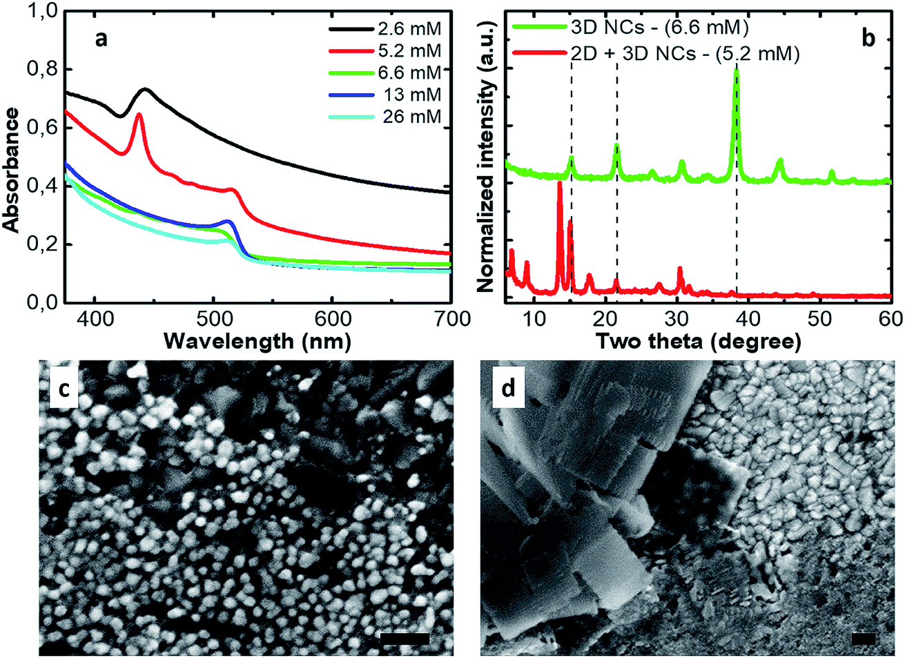 | ||
| Fig. 1 CsPbBr3 NCs were deposited on glass by the spin coating technique. (a) Absorption spectra of NCs obtained by using different concentrations of the Cs2CO3 precursor; (b) XRD patterns of only 3D NCs (green line) and a mixture of 2D platelets and 3D NCs (red line). The HR-SEM images of the colloidal crystals measured in (b) show the (c) absence and (d) presence of 2D components. Scale bar 200 nm. | ||
We have also tested the variation in concentration of PbBr2 dissolved in IPA:PrAc:BuAm. Starting from 0.50 M, we decreased the concentration until 0.20 M.
In Fig. 2a we show the (100) diffraction peak which shows an enhancement of the crystal mean domain size as we reduce the PbBr2 concentration. In Table 1 we report the mean domain size as a function of the precursor concentration, given by the Scherrer equation, analyzing the (100) XRD peak. As the concentration decreases, the mean domain grows. The onset of the absorption spectrum, in agreement, shows a more defined excitonic transition as the crystal size increases35 indicating a higher level of order (Fig. 2b). In Fig. 2c we show the current density–voltage (J–V) characteristics obtained from solar cells made of thin films with different mean domain sizes of NCs. Initially, as the size increases, the photocurrent grows as well, until an optimum crystal size of about 28 nm. Then, for crystals larger than 50 nm, the thin film becomes insulating because of a worse packing during the film deposition.
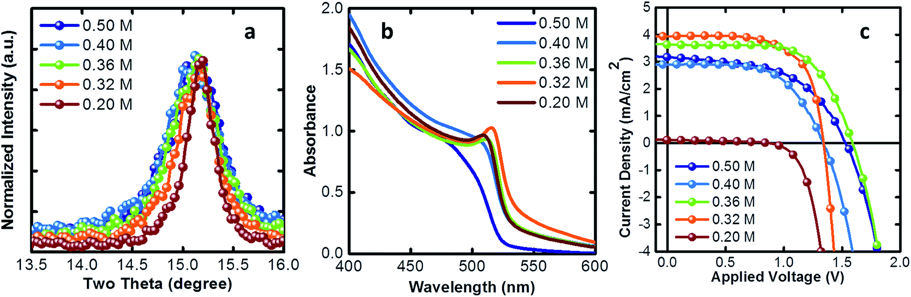 | ||
| Fig. 2 PbBr2 concentration dependence analysis. (a) XRD normalized main peak (100) used to calculate the mean domain size with the Scherrer equation, (b) absorbance and (c) J–V characteristics of solar cells. | ||
| PbBr2 concentration (M) | Mean domain size (nm) | J sc (mA cm−2) | V oc (V) | FF (%) | PCE (%) |
|---|---|---|---|---|---|
| 0.50 | 18.32 | 3.17 | 1.53 | 53.2 | 2.59 |
| 0.40 | 23.66 | 2.90 | 1.34 | 60.1 | 2.37 |
| 0.36 | 28.26 | 3.63 | 1.60 | 64.3 | 3.73 |
| 0.32 | 38.55 | 3.94 | 1.34 | 66.2 | 3.56 |
| 0.20 | 60.40 | 0.13 | 0.88 | 39.6 | 0.04 |
The size of the NCs is also important to achieve good photo-stability of the thin films. Fig. 3 shows the relative PL quantum yield, calculated as the integrated PL intensity normalized with the excitation intensity, of thin films fabricated with NCs of different sizes. When measuring from low to high excitation intensities (solid lines) and then in reverse order (dashed lines), we observe a reduction of the emission efficiency (Fig. 3a) resulting from photo-induced trap formation36 in thin films made with bigger NCs (ca. 60 nm). The sample with an optimum size of about 28 nm does not show any important changes as a function of excitation intensity. Motti et al. have recently demonstrated that efficient surface passivation of polycrystalline perovskite thin films not only reduces the density of defect states, but also photo-stabilizes the perovskite thin films.37
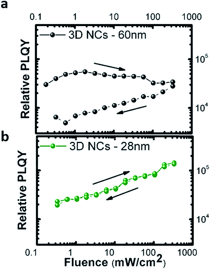 | ||
| Fig. 3 Relative photoluminescence quantum yield as a function of fluence for thin films made from NCs of (a) 60 nm and (b) 28 nm. Measurements are carried out with increasing (solid line) and decreasing fluence (dashed lines). Excitation source: 405 nm CW laser. | ||
Thus, the results shown in Fig. 3 reveal an optimum size of NCs which allows for a good passivation of the NC surface in solution and good passivation of grain boundaries in the thin films.
Another important parameter to control the NC packing is the nature of the dispersing solvent which allows a higher or lower degree of aggregation of the particles in the ink. Avoiding pre-aggregation of the particles can present an advantage during the deposition of the ink, allowing for a controllable thickness and homogeneous films. Toluene-dispersed NCs are the most stable in time and present the smallest size. When increasing the polarity, dispersing the NCs in propan-2-ol (isopropanol), they become more unstable and the size varies up to 40 nm (values calculated with the Scherrer equation from the XRD peak shown in Fig. 4a and refer to the average of the mean domain sizes of the crystallites) negativelly affecting the devices performances (ESI, Fig. S1†). The solvent boiling point is another important parameter for the thin film morphology upon printing, and it must be taken into account. To compromise among the tendency of aggregation of NCs in dispersion, the use of a solvent with a low enough boiling point for printing, and the attempt to maintain a low level of toxicity of the solvent used, we tested a mixture of two solvents, propan-2-ol and toluene with a ratio of 2:1 (UV-vis spectrum in Fig. 4b). The presence of propan-2-ol allows us to decrease the boiling point and to speed up the drying process between two consecutive bar coated layers and improve the morphology with respect to toluene only. The presence of toluene as a dispersant does not allow a complete aggregation of the NCs in the ink, obtaining a final NC mean domain size of around 34 nm (calculated using the Scherrer equation, Fig. 4a).
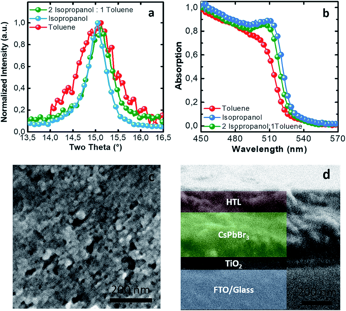 | ||
| Fig. 4 NCs dispersed in different solvents. (a) XRD normalized peak at 15.2° used to calculate the average of domain sizes by the Scherrer equation and (b) absorbance of thin films fabricated from NC dispersed in toluene, isopropanol and a mixture of the two. (c) Top view morphology of the bar coated NC layer and (d) cross-section of a complete solar cell device. | ||
After learning how to control the synthesis, the effect of the solvents used on the NC size and the properties of the dispersant solvent, we were able to print the inks, obtaining a good morphology and good smoothness of the active layer as shown in Fig. 4c. This permitted us to fabricate standard structured solar cells using the bar coating technique with a 1 cm2 active area and a sandwich structure as shown in Fig. 4d.
The J–V characteristics, shown in Fig. 5a, are achieved by printing 5 consecutive layers, with a waiting time of 2 minutes between different layers. This procedure permits us to achieve a thickness of the active layer equal to 300 nm and the absorbance is shown in the ESI, Fig. S2.† The speed of the bar is set to 30 mm s−1 with a groove path of 4 μm. The solar cells were tested under 0.99 sun with a scan rate of 0.01 V s−1, obtaining Jsc = 2.48 mA cm−2, Voc = 1.31 V, FF% = 63% and PCE% = 2.11%. In Fig. 5b we tested the device at the maximum power point in air, with 65% humidity (without any kind of encapsulation) for 10 minutes, and the performances were not affected, thus showing no transient behavior.
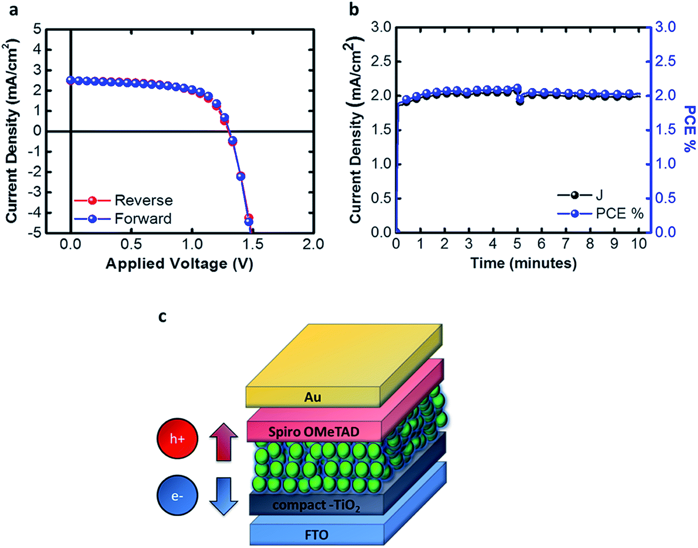 | ||
| Fig. 5 (a) Current density (J)–voltage (V) curve in forward (blue line) and reverse (red line) bias under 0.99 sun. Scan rate 0.01 V s−1. (b) Current density (J) (black line) and PCE% (blue line) at the maximum power point as a function of time. (c) Sketch of solar cell device architecture. | ||
In conclusion, we have demonstrated how to control the size and shape of colloidal perovskite NCs and the properties of relative inks in order to print thin films with good optoelectronic properties. We show that to achieve a good NC packing, and therefore conductivity, one needs to have a full control of the particle size, which will depend on the relative precursor concentration, ligand concentration and solvent polarity. Such a fine tuning of the synthetic procedure allows us to print 1 cm2 solar cells.
Conflicts of interest
There are no conflicts to declare.Acknowledgements
The authors thank Prof. Liberato Manna for useful discussions.References
- G. Giorgi, J.-I. Fujisawa, H. Segawa and K. J. Yamashita, Cation Role in Structural and Electronic Properties of 3D Organic–Inorganic Halide Perovskites: A DFT Analysis, J. Phys. Chem. Lett., 2013, 4, 4213 CrossRef CAS PubMed.
- G. Giorgi, J. I. Fujisawa, H. Segawa and K. Yamashita, Small Photocarrier Effective Masses Featuring Ambipolar Transport in Methylammonium Lead Iodide Perovskite: A Density Functional Analysis, J. Phys. Chem. Lett., 2013, 4(24), 4213–4216 CrossRef CAS PubMed.
- T. Leijtens, S. D. Stranks, G. E. Eperon, R. Lindblad, E. M. Johansson, I. J. McPherson, H. Rensmo, J. M. Ball, M. M. Lee and H. J. Snaith, Electronic properties of meso-superstructured and planar organometal halide perovskite films: charge trapping, photodoping and carrier mobility, ACS Nano, 2014, 8, 7147–7155 CrossRef CAS PubMed.
- A. Miyata, A. Mitioglu, P. Plochocka, O. Portugall, J. T. W. Wang, S. D. Stranks, H. J. Snaith and R. J. Nicholas, Direct Measurement of the Exciton Binding Energy and Effective Masses for Charge carriers in an Organic–Inorganic Tri-halide Perovskite, Nat. Phys., 2015, 11, 582 Search PubMed.
- M. B. Johnston and L. M. Herz, Hybrid Perovskites for Photovoltaics: Charge-Carrier Recombination, Diffusion, and Radiative Efficiencies, Acc. Chem. Res., 2016, 49, 146–154 CrossRef CAS PubMed.
- T. M. Koh, K. Fu, Y. Fang, S. Chen, T. C. Sum, N. Mathews, S. G. Mhaisalkar, P. P. Boix and T. Baikie, Formamidinium-Containing Metal-Halide: An Alternative Material for Near-IR Absorption Perovskite Solar Cells, J. Phys. Chem. C, 2014, 118(30), 16458–16462 CrossRef CAS.
- N. G. Park, Perovskite solar cells: an emerging photovoltaic technology, Mater. Today, 2015, 2, 65–72 CrossRef.
- A. Kojima, K. Teshima, Y. Shirai and T. Miyasaka, Organometal Halide Perovskites as Visible-Light Sensitizers for Photovoltaic Cells, J. Am. Chem. Soc., 2009, 131, 6050–6051 CrossRef CAS PubMed.
- M. M. Lee, J. Teuscher, T. Miyasaka, T. N. Murakami and H. J. Snaith, Efficient hybrid solar cells based on meso-superstructured organometal halide perovskites, Science, 2012, 338, 643–647 CrossRef CAS PubMed.
- H. S. Kim, C. R. Lee, J. H. Im, K. B. Lee, T. Moehl, A. Marchioro, S. J. Moon, R. Humphry-Baker, J. H. Yum, J. E. Moser, M. Grätzel and N. G. Park, Lead iodide perovskite sensitized all-solid-state submicron thin film mesoscopic solar cell with efficiency exceeding 9%, Sci. Rep., 2012, 2, 591 CrossRef PubMed.
- P. Docampo, J. M. Ball, M. Darwich, G. E. Eperon and H. J. Snaith, Efficient organometal trihalide perovskite planar-heterojunction solar cells on flexible polymer substrates, Nat. Commun., 2013, 4, 2761 CrossRef PubMed.
- C. Tao, S. Neutzner, L. Colella, S. Marras, A. R. Srimath Kandada, M. Gandini, M. De Bastiani, G. Pace, L. Manna, M. Caironi, C. Bertarelli and A. Petrozza, 17.6% stabilized efficiency in low-temperature processed planar perovskite solar cells, Energy Environ. Sci., 2015, 8, 2365–2370 RSC.
- https://www.nrel.gov/pv/assets/pdfs/pv-efficiency-chart.20190103.pdf .
- Z. K. Tan, R. S. Moghaddam, M. L. Lai, P. Docampo, R. Higler, F. Deschler, M. Price, A. Sadhanala, L. M. Pazos, D. Credgington, F. Hanusch, T. Bein, H. J. Snaith and R. H. Friend, Bright light-emitting diodes based on organometal halide perovskite, Nat. Nanotechnol., 2014, 9, 687–692 CrossRef CAS PubMed.
- G. Li, Z.-K. Tan, D. Di, M. L. Lai, L. Jiang, J. Hua-Wei Lim, R. H. Friend and N. C. Greenham, Efficient Light-Emitting Diodes Based on Nanocrystalline Perovskite in a Dielectric Polymer Matrix, Nano Lett., 2015, 15(4), 2640–2644 CrossRef CAS PubMed.
- Z. Xiao, R. A. Kerner, L. Zhao, N. L. Tran, K. M. Lee, T.-W. Koh, G. D. Scholes and B. P. Rand, Efficient perovskite light-emitting diodes featuring nanometre-sized crystallites, Nat. Photonics, 2017, 11, 108–115 CrossRef CAS.
- K. Lin, J. Xing, L. N. Quan, F. Pelayo García de Arquer, X. Gong, J. Lu, L. Xie, W. Zhao, D. Zhang, C. Yan, W. Li, X. Liu, Y. Lu, J. Kirman, E. H. Sargent, Q. Xiong and Z. Wei, Perovskite light-emitting diodes with external quantum efficiency exceeding 20 percent, Nature, 2018, 562, 245–248 CrossRef CAS PubMed.
- W. Xu, Q. Hu, S. Bai, C. Bao, Y. Miao, Z. Yuan, T. Borzda, A. J. Barker, E. Tyukalova, Z. Hu, M. Kawecki, H. Wang, H. Yan, X. Liu, X. Shi, K. Uvdal, M. Fahlman, W. Zhang, M. Duchamp, J. M. Liu, A. Petrozza, J. Wang, L. M. Liu, W. Huang and F. Gao, Rational molecular passivation for high-performance perovskite light-emitting diodes, Nat. Photonics, 2019, 13, 418–424 CrossRef CAS.
- L. Dou, Y. M. Yang, J. You, Z. Hong, W. H. Chang, G. Li and Y. Yang, Solution-processed hybrid perovskite photodetectors with high detectivity, Nat. Commun., 2014, 5, 5404 CrossRef CAS PubMed.
- M. I. Saidaminov, V. Adinolfi, R. Comin, A. L. Abdelhady, W. Peng, I. Dursun, M. Yuan, S. Hoogland, E. H. Sargent and O. M. Bakr, Planar-integrated single-crystalline perovskite photodetectors, Nat. Commun., 2015, 6, 8724 CrossRef CAS PubMed.
- V. Venugopalan, R. Sorrentino, P. Topolovsek, D. Nava, S. Neutzner, G. Ferrari, A. Petrozza and M. Caironi, High-Detectivity Perovskite Light Detectors Printed in Air from Benign Solvents, Chem, 2019, 5, 1–13 Search PubMed.
- G. Xing, N. Mathews, S. S. Lim, N. Yantara, X. Liu, D. Sabba, M. Grätzel, S. Mhaisalkar and T. C. Sum, Low-temperature solution-processed wavelength-tunable perovskites for lasing, Nat. Mater., 2014, 13, 476–480 CrossRef CAS PubMed.
- B. R. Sutherland, S. Hoogland, M. M. Adachi, C. T. Wong and E. H. Sargent, Conformal organohalide perovskites enable lasing on spherical resonators, ACS Nano, 2014, 8(10), 10947–10952 CrossRef CAS PubMed.
- F. Deschler, M. Price, S. Pathak, L. E. Klintberg, D. D. Jarausch, R. Higler, S. Hüttner, T. Leijtens, S. D. Stranks, H. J. Snaith, M. Atatüre, R. T. Phillips and R. H. Friend, High Photoluminescence Efficiency and Optically Pumped Lasing in Solution-Processed Mixed Halide Perovskite Semiconductors, J. Phys. Chem. Lett., 2014, 5, 1421–1426 CrossRef CAS PubMed.
- X. Y. Chin, D. Cortecchia, J. Yin, A. Bruno and C. Soci, Lead iodide perovskite light-emitting field-effect transistor, Nat. Commun., 2015, 6, 7383 CrossRef CAS PubMed.
- F. Li, C. Ma, H. Wang, W. Hu, W. Yu, A. D. Sheikh and T. Wu, Ambipolar solution-processed hybrid perovskite phototransistors, Nat. Commun., 2015, 6, 8238 CrossRef PubMed.
- W. Yu, F. Li, L. Yu, M. R. Niazi, Y. Zou, D. Corzo, A. Basu, C. Ma, S. Dey, M. L. Tietze, U. Buttner, X. Wang, Z. Wang, M. N. Hedhili, C. Guo, T. Wu and A. Amassian, Single crystal hybrid perovskite field-effect transistors, Nat. Commun., 2018, 9, 5354 CrossRef PubMed.
- Q. A. Akkerman, M. Gandini, F. Di Stasio, P. Rastogi, F. Palazon, G. Bertoni, G. M. Ball, M. Prato, A. Petrozza and L. Manna, Strongly emissive perovskite nanocrystal inks for high-voltage solar cells, Nat. Energy, 2016, 2, 16194 CrossRef.
- Z. Liang, S. Zhao, Z. Xu, B. Qiao, P. Song, D. Gao and X. Xu, Shape-Controlled Synthesis of All-Inorganic CsPbBr3 Perovskite Nanocrystals with Bright Blue Emission, ACS Appl. Mater. Interfaces, 2016, 8(42), 28824–28830 CrossRef CAS PubMed.
- A. Dutta, S. Kumar, D. Samrat, S. Das Adhikari and N. Pradhan, Tuning the Size of CsPbBr3 Nanocrystals: All at One Constant Temperature, ACS Energy Lett., 2018, 3(2), 329–334 CrossRef CAS.
- V. D'Innocenzo, A. R. S. Kandada, M. De Bastiani, M. Gandini and A. Petrozza, Tuning the Light Emission Properties by Band Gap Engineering in Hybrid Lead Halide Perovskite, J. Am. Chem. Soc., 2014, 136(51), 17730–17733 CrossRef PubMed.
- G. Almeida, L. Goldoni, Q. Akkerman, Z. Dang, A. H. Khan, S. Marras, I. Moreels and L. Manna, Role of Acid–Base Equilibria in the Size, Shape, and Phase Control of Cesium Lead Bromide Nanocrystals, ACS Nano, 2018, 12(2), 1704–1711 CrossRef CAS PubMed.
- G. Nedelcu, L. Protesescu, S. Yakunin, M. I. Bodnarchuk, M. J. Grotevent and M. V. Kovalenko, Fast Anion-Exchange in Highly Luminescent Nanocrystals of Cesium Lead Halide Perovskites (CsPbX3, X = Cl, Br, I), Nano Lett., 2015, 15(8), 5635–5640 CrossRef CAS PubMed.
- A. S. Verma and V. K. Jindal, Lattice constant of cubic perovskites, J. Alloys Compd., 2009, 485, 514–518 CrossRef CAS.
- G. Grancini, A. R. S. Kandada, J. M. Frost, A. J. Barker, M. De Bastiani, M. Gandini, S. Marras, G. Lanzani, A. Walsh and A. Petrozza, Role of microstructure in the electron–hole interaction of hybrid lead halide perovskites, Nat. Photonics, 2015, 9, 695–701 CrossRef CAS PubMed.
- S. G. Motti, M. Gandini, A. J. Barker, J. M. Ball, A. R. S. Kandada and P. Petrozza, Photoinduced Emissive Trap States in Lead Halide Perovskite Semiconductors, ACS Energy Lett., 2016, 14, 726–730 CrossRef.
- S. M. Motti, D. Meggiolaro, A. J. Barker, E. Mosconi, C. A. R. Perini, J. M. Ball, M. Gandini, M. Kim, F. De Angelis and A. Petrozza, Controlling competing photochemical reactions stabilizes perovskite solar cells, Nat. Photonics, 2019, 13, 532–539 CrossRef CAS.
Footnote |
| † Electronic supplementary information (ESI) available. See DOI: 10.1039/c9se00502a |
| This journal is © The Royal Society of Chemistry 2020 |