
 Open Access Article
 This Open Access Article is licensed under a Creative Commons Attribution-Non Commercial 3.0 Unported Licence
Constructing orderly crystal orientation with a bidirectional coordinator for high efficiency and stable perovskite solar cells†
Jaehwi
Lee‡
a,
Yun Seop
Shin‡
 ab,
Elham
Oleiki‡
c,
Jongdeuk
Seo
a,
Jina
Roe
a,
Dongmin
Lee
b,
Yeonjeong
Lee
a,
Taehee
Song
a,
Hyungsu
Jang
a,
Ji Won
Song
b,
Woosuk
Lee
b,
Geunsik
Lee
*c,
Jin Young
Kim
*ab and
Dong Suk
Kim
*ab
ab,
Elham
Oleiki‡
c,
Jongdeuk
Seo
a,
Jina
Roe
a,
Dongmin
Lee
b,
Yeonjeong
Lee
a,
Taehee
Song
a,
Hyungsu
Jang
a,
Ji Won
Song
b,
Woosuk
Lee
b,
Geunsik
Lee
*c,
Jin Young
Kim
*ab and
Dong Suk
Kim
*ab
aSchool of Energy and Chemical Engineering, Ulsan National Institute of Science and Technology (UNIST), Ulsan 44919, Republic of Korea. E-mail: jykim@unist.ac.kr
bGraduate School of Carbon Neutrality, Ulsan National Institute of Science and Technology (UNIST), Ulsan 44919, Republic of Korea. E-mail: kimds@unist.ac.kr
cCenter for Superfunctional Materials, Department of Chemistry, Ulsan National Institute of Science and Technology (UNIST), Ulsan 44919, Republic of Korea. E-mail: gslee@unist.ac.kr
First published on 11th July 2024
Abstract
A well-developed perovskite crystal at the beginning of a crystal lattice facilitates favourable growth orientation for efficient charge transport and the elimination of buried interfaces. However, rapid and uncontrollable crystallization of perovskites poses significant challenges in achieving desired growth orientations and controlling the growth direction during crystallization, necessitating the establishment of optimal substrate conditions. In this study, we propose a bidirectional coordination strategy involving the introduction of cesium trifluoroacetate (CsTFA) onto a tin dioxide (SnO2) surface. Treatment with CsTFA facilitates the passivation of SnO2 vacancies via COOH–Sn while concurrently forming intermolecular interactions with overlying perovskite crystals, manifested as CF3⋯H–N for formamidinium (FA+) and CF3⋯I–Pb, respectively. These interactions initiate the well-established beginning of the perovskite crystals and promote their vertical growth. Consequently, vertically grown perovskite crystals exhibit reduced tensile strain and fewer crystalline defects. Furthermore, a benign buried interface between the perovskite and underlying SnO2 mitigates detrimental damage, thereby suppressing non-radiative recombination losses. This synergetic bidirectional coordination contributes to the fabrication of perovskite solar cells with a maximum power conversion efficiency of 25.60% (certified at 25.39%) and long-term stability under light illumination.
Broader contextThe detrimental buried interface, stemming from discrepancies in thermal expansion coefficients of the substrate or the erratic formation of perovskite crystals, poses a significant barrier to achieving further enhancements in both efficiency and stability. Presently, various methodologies have been investigated to improve such buried interfaces, with a significant emphasis on additive engineering. Trifluoroacetate (TFA−) pseudo-halide anions have been specifically introduced into the perovskite or at the interface, leveraging their elevated binding affinity for iodide vacancies and carboxylate functionality (–COO−). In this study, we have unveiled that TFA− anions serve not only as passivation agents at the buried interface but also as bidirectional coordinators, considering the hydrogen bonding capabilities of fluorine-organic head groups. The simultaneous coordination of the anchoring group (–COO−) and the organic head group (–CF3) with tin dioxide (SnO2) and the perovskite lattice (formamidinium and lead cations), respectively, facilitates orderly initiation of crystals with a favourable growth orientation, thereby promoting their vertical growth. The resulting perovskite films, devoid of the buried interface and residual tensile strain, attain a champion power conversion efficiency (PCE) of 25.60%. Furthermore, the unencapsulated device maintains over 80% of its initial PCE after 1000 hours under prolonged light illumination. |
Introduction
Organic–inorganic lead halide perovskite solar cells (PSCs) have demonstrated significant commercial potential, surpassing 26% in power conversion efficiencies (PCEs) for small-area single-junction cells and achieving over 33% for perovskite-silicon tandem cells.1–3 Ensuring stability is essential for the rapid commercialization of PSCs, necessitating the efficient mitigation of degradation at defect sites within both the upper perovskite interface and the bulk region. Therefore, extensive research has been conducted on surface passivation, additive engineering, or post-treatment methods to stabilize both the interface and the bulk region of perovskites.4–7Recently, there has been a pronounced surge in research concerning buried interfaces between perovskite films and the underlying electron transport layers (ETLs) for n–i–p structured devices.8–10 The buried interface, where defects are prone to form compared to the bulk of perovskites, instigates losses in carrier recombination, thereby constraining further enhancements in efficiency and stability.11,12 Although several commitments to addressing problematic issues have ultimately resulted in achieving a PCE exceeding 26%, the stability concerns stemming from buried interfaces continue to be a paramount focus of attention.13,14
Textured fluorine-doped tin oxide (FTO) substrates are primarily employed, leveraging their capability to enhance light absorption.15 However, on the textured FTO substrates, inevitable distortion or imperfections in perovskite crystals arise during rapid and uncontrollable crystallization processes, predisposing the formation of buried interfaces.16,17 Furthermore, beyond the texturing of substrates, the disordered growth of periodic perovskite crystals, induced by mismatches in thermal expansion coefficients or lattice discrepancies, further augments the formation of buried interfaces.18–20 The presence of the buried interface entails several adverse effects, including unfavourable lattice strain, poor crystallinity, high defect density, and compromised interfacial adhesion.11,21 Among these effects, particularly, induced lattice strain within the perovskite lattice impedes the behaviour of charge carriers and even alters its electrical properties through band gap shifting.22
Several methodologies have been demonstrated to refine the buried interface. For instance, Luo et al. introduced a novel conductive perovskite, SrSnO3, to serve as the ETL, offering more ordered starting points for the epitaxial growth of perovskite crystals.8 Besides, Wang et al. employed a 4-chloro-3-sulfamoylbenzoic acid additive to construct an oriented molecular bridge.23 This bridge enables multiple coordination with both the ETL and perovskite, thereby enhancing the energy order at the heterointerface.24,25 Their common strategy involves aligning the arrangement of perovskite crystals growing at the interface of the ETL. Periodic perovskite crystals commence their growth at the surface of underlying ETLs, culminating in the termination of this growth at the upper surface, where numerous interfacial defects are present.26,27 Moreover, the initial disorder in perovskite crystals at the beginning directly reflects the orientation of their upper surface, thus potentially triggering severe interfacial defects.28,29 It is feasible to readily passivate these defects through post-treatment procedures, whereas controlling such bottom surface remains challenging due to its lack of exposure compared to the upper surface.4,6 Accordingly, the construction of ordered perovskite crystals on the bottom surface can represent a realistic approach to mitigating the adverse effects of the buried interface. This underscores the importance of establishing an optimal ETL substrate to address this issue.
In this study, we have demonstrated that the insertion of trifluoroacetate (TFA−) pseudo-halide anions into the buried interface between the SnO2 ETL and perovskite layer plays a vital role in the efficiency and stability of PSCs. TFA− pseudo-halide anions have been extensively employed in PSCs as either interface passivation agents or additives within the perovskite layer,30–32 leveraging their elevated binding affinity toward iodide vacancies.33–36 Our findings reveal another pivotal role of TFA− pseudo-halide anions; they could serve as bidirectional coordinators, facilitating the organized nucleation of periodic perovskite crystals. For a comprehensive exploration of the interplay at the buried interface, we deliberately selected diverse molecules, including cesium formate (CsFo), cesium acetate (CsAc), and CsTFA, meticulously scrutinizing their impact on the interaction. Each molecule possesses a carboxylate group (–COO−), serving as an anchoring moiety on the SnO2 ETL, while the head groups of –H (Fo−), –CH3 (Ac−), and –CF3 (TFA−) undergo chemical interactions with the overlying perovskite layer. Compared to the bare SnO2 ETL, the incorporation of these pseudo-halide anions demonstrates superior electrical and morphological properties, particularly with TFA−, showcasing the strongest interactions attributed to potential hydrogen and halogen bonding interactions of the –CF3 head group with the formamidinium (FA+) cation and Pb–I, respectively. This bidirectional coordination enables the orderly initiation of periodic perovskite crystals, thereby leading to their vertical growth. The resultant perovskite crystals exhibit diminished residual tensile strain and monolithic grains with fewer crystalline defects. Additionally, the attenuated energetic disorder hinders the formation of non-radiative pathways, thereby exemplifying the presence of long-lived charge carriers. In consequence, highly crystalline perovskite films devoid of the buried interface achieve a champion PCE of 25.60% (certified at 25.39%) and sustain over 80% of its initial PCE under prolonged light illumination after 1000 hours.
Results and discussion
We prepared a bilayer substrate comprising compact titanium dioxide (c-TiO2)/tin dioxide (SnO2) to function as an electron transport layer (ETL), utilizing the methods previously reported in the literature (referred to as control-SnO2).15 Then, we implemented a procedure involving the treatment of CsX with varying pseudo-halide anions (X = Fo−, Ac−, and TFA−) on the ETL substrate prior to depositing the perovskite films (referred to as CsX-treated SnO2) (Fig. 1a). The embedded Cs+ ions, treated with CsX, have the capability to integrate into the perovskite lattice near the buried interface during the spin-coating of the perovskite solution.9 This integration serves to stabilize the FA-based perovskite structure by ensuring an optimal tolerance factor conducive to sustaining the cubic phase.37,38 To evaluate the bidirectional interactions of pseudo-halide anions with both the underlying SnO2 substrate and the overlying perovskite films, we carried out Fourier transform infrared spectroscopy (FTIR) measurements (Fig. 1b–d).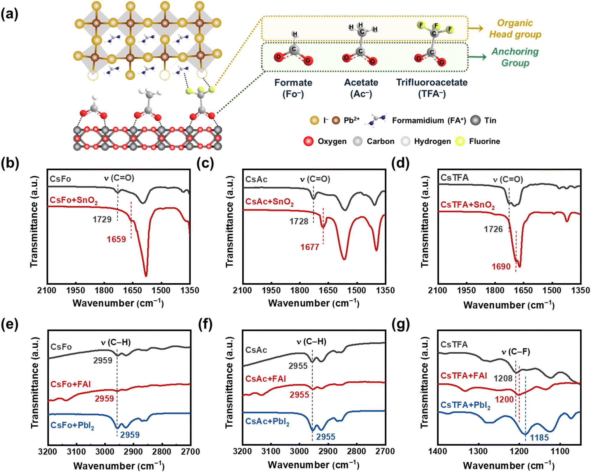 | ||
| Fig. 1 (a) Schematic illustration of the CsX (X = Fo−, Ac−, and TFA−) treatment process applied to the SnO2 ETL. FTIR spectra of CsX, CsX–SnO2, CsX–FAI, and CsX–PbI2, (b) and (e) CsFo, (c) and (f) CsAc, and (d) and (g) CsTFA. | ||
First, we observed stretching vibration peaks corresponding to a carbonyl functional group (C![[double bond, length as m-dash]](https://www.rsc.org/images/entities/char_e001.gif) O) at 1729, 1728, and 1726 cm−1 for CsFo, CsAc, and CsTFA precursors, respectively. However, after treating CsX onto the SnO2 ETLs, these distinctive peaks exhibited notable shifts to 1659, 1677, and 1690 cm−1, respectively, indicative of the existence of COOH–Sn groups on the surface of SnO2.23,39 Further evidence of the chemical interaction between the CO groups and SnO2 is discernible in the X-ray photoelectron spectroscopy (XPS) spectra (Fig. S1a, ESI†). As shown in Fig. S1a (ESI†), control-SnO2 films showed an XPS spectrum featuring two prominent peaks at 487.46 and 495.93 eV, assigned to Sn 3d5/2 and Sn 3d3/2, respectively. Conversely, XPS spectra of all CsX-treated SnO2 films revealed a shift of the Sn 3d peaks to lower binding energies. This observed peak shift towards lower binding energies provides further support for the aforementioned chemical interaction between the CO groups and underlying SnO2, elucidating the effect of CsX treatment in passivating oxygen vacancies on the SnO2 surface. Other studies have also reported similar shifts when the carbonyl group coordinates with SnO2.23,39,40
O) at 1729, 1728, and 1726 cm−1 for CsFo, CsAc, and CsTFA precursors, respectively. However, after treating CsX onto the SnO2 ETLs, these distinctive peaks exhibited notable shifts to 1659, 1677, and 1690 cm−1, respectively, indicative of the existence of COOH–Sn groups on the surface of SnO2.23,39 Further evidence of the chemical interaction between the CO groups and SnO2 is discernible in the X-ray photoelectron spectroscopy (XPS) spectra (Fig. S1a, ESI†). As shown in Fig. S1a (ESI†), control-SnO2 films showed an XPS spectrum featuring two prominent peaks at 487.46 and 495.93 eV, assigned to Sn 3d5/2 and Sn 3d3/2, respectively. Conversely, XPS spectra of all CsX-treated SnO2 films revealed a shift of the Sn 3d peaks to lower binding energies. This observed peak shift towards lower binding energies provides further support for the aforementioned chemical interaction between the CO groups and underlying SnO2, elucidating the effect of CsX treatment in passivating oxygen vacancies on the SnO2 surface. Other studies have also reported similar shifts when the carbonyl group coordinates with SnO2.23,39,40
Following the adsorption of CsX (anchoring group) on the SnO2 surface, the potential for additional chemical interactions between the opposing sites (organic head group) of CsX molecules and the perovskite lattices becomes apparent (Fig. 1a). As shown in Fig. 1e–g, we conducted FTIR measurements on the mixture of CsX with FAI and PbI2, respectively, to investigate the possible coordination of pseudo-halide anions with overlying perovskite films at the buried interface.36,41 Meanwhile, the position of stretching vibration peaks associated with the opposing sites, C–H groups in CsFo and CsAc, remains unchanged following the addition of FAI and PbI2 into CsX, respectively. It implies less pronounced interactions of pseudo-halide anions, Fo− and Ac−, with the perovskite lattice in the thin film states. However, in the case of TFA−, the stretching vibration peaks corresponding to the C–F groups, which are the head group sites of TFA−, notably shift towards lower wavenumbers upon addition of both FAI and PbI2, respectively (Fig. 1g). The fluorine-containing pseudo-halide, TFA−, facilitates the formation of hydrogen bonding with organic cations, FA+,42–44 as well as halogen bonding with Pb–I36,45,46 as illustrated in Fig. 1a. To confirm these interactions at the buried interface, XPS measurements were performed on perovskite films peeled off from the SnO2 ETLs. It is evidenced by the shift of characteristic N 1s and Pb 4f peaks for FAI and PbI2, respectively, along with the disappearance of the peak for uncoordinated Pb2+, in the measured XPS spectra (Fig. S1b and c, ESI†). Considering these results, the TFA− anions introduced can serve as bidirectional coordinators between the SnO2 ETL and the perovskite crystals, which would foster the orientation and crystalline properties of perovskite films.
Based on the above results, cross-sectional scanning electron microscopy (SEM) measurements were conducted to gain insights into the orientation of perovskite crystals (Fig. 2a). The perovskite film on the CsTFA-treated SnO2 ETL exhibits a conformal growth pattern featuring monolithic grains, in contrast to that observed on the control-SnO2 ETL. The bidirectional coordination of TFA− with both SnO2 and the perovskite crystal may initiate the vertical growth of the bulk perovskite film, resulting in the distinctive crystallinity observed in the perovskite films, as revealed in the X-ray diffraction (XRD) patterns (Fig. S2a, ESI†). The XRD patterns revealed two prominent diffraction peaks at 14.0° and 28.2°, assigned to the (001) and (002) planes of the FAPbI3 perovskite crystal, respectively. The enhanced crystallinity of perovskite films can be further corroborated by both the heightened intensities of two prominent diffraction peaks and the narrowed full width at half maximum (FWHM) observed in the XRD patterns (Fig. S2b, ESI†). Furthermore, top-view SEM images reveal compact and pinhole-free perovskite films on the CsTFA-treated SnO2 ETL (Fig. S3, ESI†). Meanwhile, as a consequence of increased hydrophobicity resulting from the exposed fluorine-containing TFA− pseudo-halides through CsTFA treatment (Fig. S4, ESI†),47,48 the perovskite film deposited on the ETL substrate under such treatment displays the enlarged grains (average grain size: 1.49 μm) compared to that on the control-SnO2 ETL (average grain size: 1.03 μm) (Fig. S5, ESI†). The exposed Fo− and Ac− also affected the overlying perovskite films by enlarging the grains. The perovskite film formed in this manner on the CsTFA-treated SnO2 also exhibits a smooth surface morphology. As observed in the atomic force microscopy (AFM) image (Fig. S6, ESI†), the root-mean-square (Rq) of 47.8 nm for the perovskite film on the control-SnO2 decreased to 36.1 nm on the CsTFA-treated SnO2.
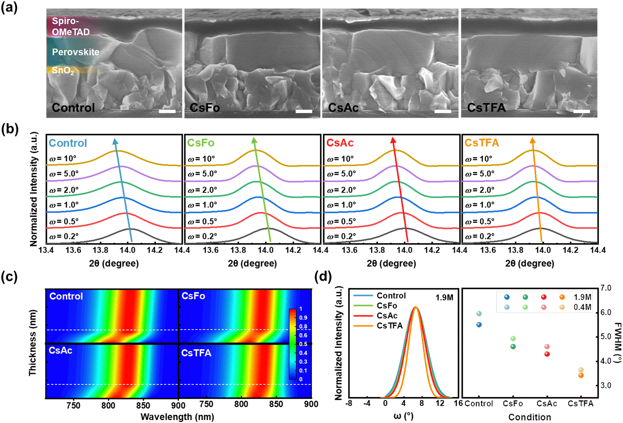 | ||
| Fig. 2 (a) Cross-sectional SEM images of the perovskite films deposited on the control- and CsX-treated SnO2, configured as FTO/control- and CsX-treated SnO2/Perovskite/Spiro-OMeTAD. (the scale bar is 200 nm). (b) GIXRD spectra of the perovskite films deposited on the control- and CsX-treated SnO2 upon varying the grazing incidence angle from 0.2° to 10°. (c) Normalized PL spectra upon varying the thickness of the perovskite films deposited on the control- and CsX-treated SnO2. (The thickness ranges from 0 to 600 nm.) (d) XRD rocking curves of the perovskite films (with a concentration of 1.9 M) deposited on the control- and CsX-treated SnO2 (left). FWHM values of XRD rocking curves of perovskite films with different concentrations, 0.4 M and 1.9 M, deposited on the control- and CsX-treated SnO2 (right). | ||
Alongside crystallinity, the manifestation of residual strain emerges as another pivotal determinant impacting the overlying perovskite film, influenced by the altered substrate characteristics. To investigate the residual strain present within the perovskite films, depth-resolved grazing incidence X-ray diffraction (GIXRD) measurements were performed by varying the grazing incidence angle (ω) from 0.2° to 10° (Fig. 2b). As the grazing incidence angle increases, the diffraction peaks corresponding to the (001) plane of the perovskite film on the control-SnO2 ETL gradually shift towards lower angles, from 14.02° to 13.93°. In contrast, the variation of diffraction peaks with respect to the grazing incidence angle was found to be less pronounced in the perovskite film on the CsTFA-treated SnO2 ETL. These outcomes imply the presence of residual strain within the perovskite film deposited on the control-SnO2 ETL, whereas both the upper and bottom surfaces of the perovskite film exhibit strain-relieved conditions on the CsTFA-treated SnO2 ETL.8,49 Based on the results of GIXRD spectra, we calculated the tensile strain present within the perovskite films (Fig. S7, ESI†). The calculated tensile strain of 0.017 for the perovskite film on the control-SnO2 diminished to 0.012 on the CsTFA-treated SnO2, indicating that the perovskite film deposited on the CsTFA-treated SnO2 experiences less stress.21
Interface-induced tensile strain is well-known to expand the optical bandgap of the perovskite film, attributed to the increased lattice constant, which shifts the valence band at the bottom surface of the perovskite film.11,22 Hence, we conducted an investigation on the thickness-dependent photoluminescence (PL) measurements to demonstrate the graded bandgap distribution induced by strain within the perovskite film (Fig. 2c). The thickness of the perovskite film is contingent upon its concentration (the concentration ranges from 0.1 M to 1.9 M). For the perovskite films on the control-SnO2, under conditions where the thickness of the perovskite film exceeds 150 nm (indicated by a white dashed line), the PL exhibits independence from the thickness of the perovskite film. Conversely, when the conditions are below 150 nm, there is a noticeable progressive blue shift in PL with ∼50 meV. This shift in PL manifests as a bandgap expansion from 1.52 (for a thickness of 500 nm) to 1.57 eV (for a thickness of 50 nm) (Fig. S8 and S9, ESI†). However, the bandgap expansion observed for the perovskite films on the CsTFA-treated SnO2 is less pronounced, increasing from 1.52 (for a thickness of 500 nm) to 1.54 eV (for a thickness of 50 nm). This result distinctly suggests that residual strain near the buried interface, initiated by mismatches in the thermal expansion coefficient or crystal lattice with the underlying ETL, has been instigated on the control-SnO2 substrate.18,20
To further explore the origin of released residual strain on the CsTFA-treated SnO2 ETL, XRD rocking curve measurements were conducted on the (001) crystal plane in perovskite films with varying thicknesses (100 nm and 500 nm) (Fig. 2d, left).50 Under the thick film condition of 500 nm, the FWHM of the rocking curve for the control-SnO2 is 5.51°, which decreased to 3.42° for the CsTFA-treated SnO2, indicating an enhancement in the (001) orientation of perovskite crystals, characteristic of vertical growth on the CsTFA-treated SnO2.51 Furthermore, the same tendency can be observed for the thin film condition of 100 nm as revealed in Fig. S10 (ESI†). Meanwhile, higher FWHM values of 5.96° and 3.65° were recorded for the thin perovskite films deposited on the control- and CsTFA-treated SnO2, respectively, in comparison to those observed under the thick perovskite film condition (5.51° and 3.42° for the control- and CsTFA-treated SnO2, respectively) (Fig. 2d, right). This difference substantiates that the disordered growth of periodic perovskite crystals at the buried interface ultimately triggers the misalignment of upper perovskite crystals, thus leading to the presence of residual tensile strain within the perovskite films. The dependency of FWHM values on the thickness was found to be less pronounced under the CsTFA-treated SnO2 condition, while under the control-SnO2 condition, the FWHM value augmented as the thickness decreased. Consequently, the bidirectional coordination facilitated by TFA− initiates a well-ordered commencement for the growth of periodic perovskite crystals at the buried interface, yielding monolithically grained and strain-free perovskite films on the CsTFA-treated SnO2 ETL.
To validate the bidirectional coordination and passivating effects of CsX molecules on the perovskite, the Vienna ab initio simulation package (VASP) was utilized for density functional theory (DFT) calculations (Fig. 3 and Fig. S11, ESI†).52 First, we computed molecular adsorption energies of head groups including –H (CsFo), –CH3 (CsAc), and –CF3 (CsTFA) molecules on I top (Itop), Pb top (Pbtop), hollow site on top of surface FA ions, and bridge position between the Pb and I atoms of the PbI2-terminated FAPbI3 perovskite surface (Fig. S12–S14, ESI†). The adsorption energy (Ead) values for –CF3 molecules on the Itop, Pbtop, hollow, and Pb–I bridge sites of the FAPbI3 perovskite were determined to be −0.42, −0.46, −0.44 and −0.47 eV, respectively (Fig. 3a). These values are higher compared to those of –H and –CH3 molecules (Table S1, ESI†), indicating a stronger chemical interaction of TFA− anions with the overlying perovskite crystals, as elucidated by FTIR and XPS results (Fig. 1). In the case of the FAI-terminated FAPbI3 perovskite surface, the computed adsorption energies exhibit a comparable trend to those observed in the former case (Fig. 3b, Fig. S15–S17 and Table S2, ESI†). Among adsorption sites, particularly on hollow sites, the Ead value is not only comparable to those of other adsorption sites but also demonstrates a higher affinity for –CF3 molecules compared to others. These results further corroborate the aforementioned interactions, encompassing hydrogen bonding with FA+ and halogen bonding with Pb–I. The interactions observed between –CF3 molecules and the perovskite crystal result in a notable reduction in trap state density. Hence, we calculated the electronic structures of both the bare defective surface and the passivated surface with each of the three head group molecules (–H, –CH3, and –CF3) on a PbI2-terminated (001) surface, which includes iodine vacancies (VI) (Fig. S18, ESI†). As depicted in the density of states (DOS) of the bare defective surface on a PbI2-terminated (001) perovskite, the presence of VI generates a partially occupied defect state below the conduction band minimum (CBM), potentially serving as interfacial non-radiative recombination pathways (Fig. 3c). Following the adsorption of –CF3 molecules at the Vi sites, the Pb–F bonding, as illustrated in the insets, induces a significant upward shift of the defect states above the CBM. Although a comparable shift in defect states is observed for –H and –CH3 molecules, a more pronounced shift is evident for –CF3 molecules, attributed to the higher electronegativity of fluorine than hydrogen. There exist some occupied defect states close to the CBM for –H and –CH3 molecules, suggesting that –CF3 molecules exhibit a greater binding affinity toward interfacial defect states compared to others. This, in turn, contributes to the minimization of interfacial VOC losses in PSCs. To further elucidate the interfacial orbital coupling between the –CF3 molecule and the FAPbI3 perovskite, we also calculated the electronic band structure of the CF3CO2/FAPbI3 interface. In Fig. 3d, the states driven by the CF3CO2 molecule are denoted by red circles, and the CF3CO2/FAPbI3 interface exhibits substantial orbital mixing through interfacial orbital hybridization, which manifests as energy level splitting (magnified in the inset). Furthermore, this interfacial orbital hybridization is evident from the isosurfaces of the associated Bloch orbitals (Fig. 3d, left), validating that it enables the strong interfacial interaction between TFA− pseudo-halide anions and perovskite crystals.
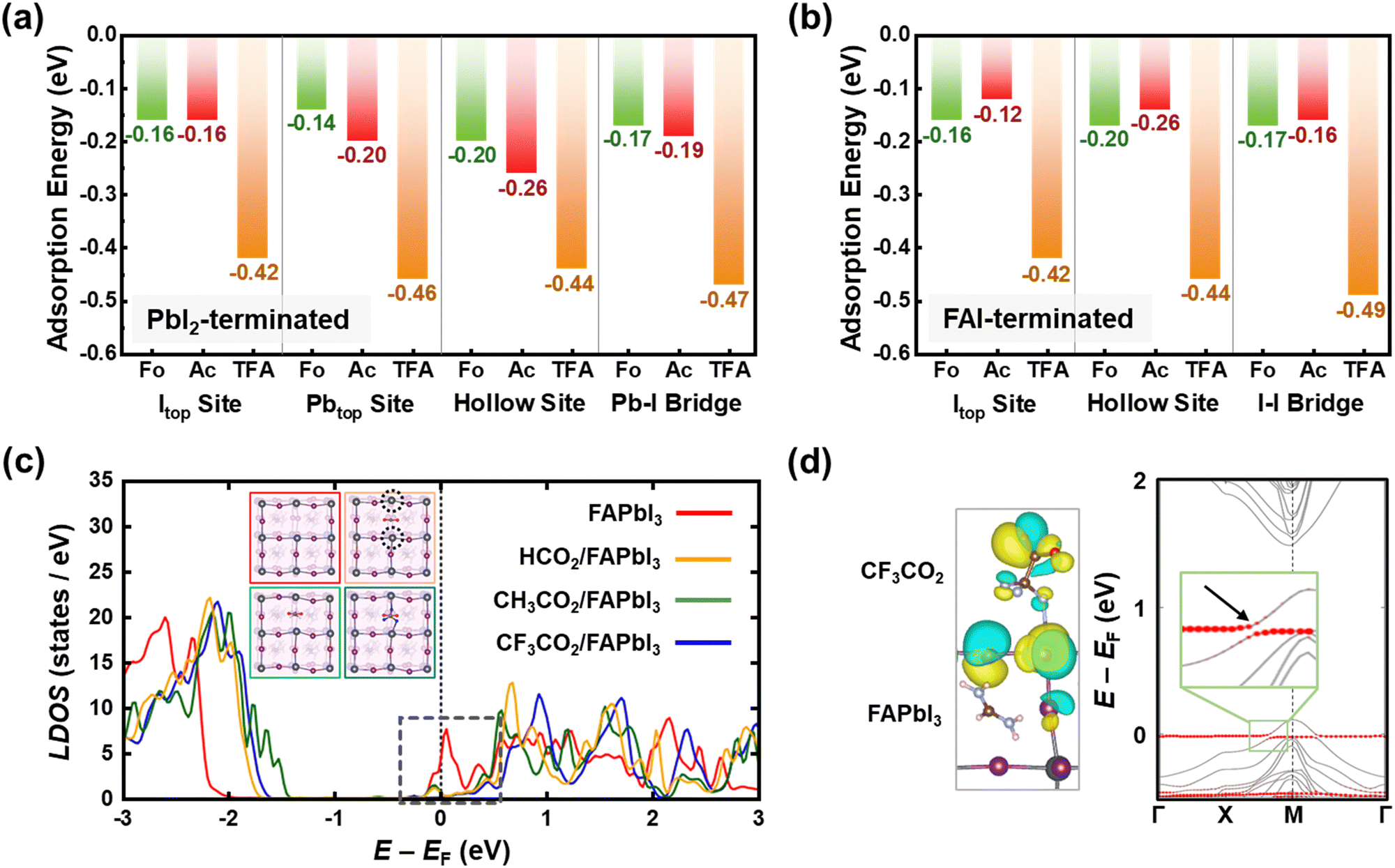 | ||
| Fig. 3 Density functional theory calculation results. (a) Calculated molecular adsorption energies of HCO2 (CsFo), CH3CO2 (CsAc), and CF3CO2 (CsTFA) molecules on I top, Pb top, hollow, and Pb–I bridge sites of the PbI2-terminated FAPbI3 perovskite. (b) Calculated molecular adsorption energies of HCO2, CH3CO2, and CF3CO2 molecules on I top, hollow, and I–I bridge sites of the FAI-terminated FAPbI3 perovskite. (c) Local density of states (LDOS) of the defective FAPbI3 top surface layer before (red) and after HCO2 adsorption (orange), CH3CO2 adsorption (green), and CF3CO2 adsorption (blue). Insets show the top view of the perovskite surface before and after molecular adsorption and under coordinated surface Pb atoms are highlighted by dotted circles. (d) Band structure of the CF3CO2/FAPbI3 interface. The contribution from CF3CO2 is shown by red circles. The inset shows the isosurfaces for an orbital indicated by the arrow, whose positive and negative parts are colored yellow and blue, respectively. Atomic color scheme: Pb (gray), I (violet), N (blue), O (red), H (pink), C (brown), and F (blue). | ||
To quantitatively estimate the trap state density (Nt) within the perovskite films, space-charge-limited charge (SCLC) measurements were carried out on the electron-only devices (EOD) with a configuration of ITO/control- and CsX-treated SnO2/Perovskite/PCPM/Ag, where ITO denotes indium tin oxide and PCBM represents [6,6]-phenyl C61 butyric acid methyl ester (Fig. 4a).53 The trap-filled limiting voltage (VTFL) was decreased from 0.254 to 0.137 V in the EOD employing the CsTFA-treated SnO2 ETL. Besides, based on these VTFL values, the Nt in the perovskite films decreased from 6.81 × 1015 cm−3 for the EOD with the control-SnO2 to 4.86 × 1015 cm−3 for the EOD with the CsTFA-treated SnO2 as corroborated by the DFT results (Fig. S19, ESI†). The reduction in trap density can be attributed to the suppression of crystalline defects and robustly crafted buried interface of the perovskite films, courtesy of the bidirectional coordination. Moreover, the aligned growth of the perovskite crystal serves to mitigate the energetic disorder inherent within the perovskite films.23 Urbach energy (Eu) measurements, conducted through ultraviolet-visible (UV-vis) absorption spectra analysis for the perovskite films (Fig. S20, ESI†),54 were utilized to explore the energetic disorder under varying ETL conditions, control- and CsX-treated SnO2. A decreased Eu value of 32 meV is observed for the perovskite films deposited on the CsTFA-treated SnO2, compared to 59 meV for that on the control-SnO2, implying the suppression of several shallow trap states within the perovskite films deposited on the CsTFA-treated SnO2 (Fig. 4b and Fig. S21, ESI†). Regarding the surface of the SnO2 substrate, the contribution of interfacial defect passivation through the formation of COOH–Sn groups to the enhancement in electrical properties of the perovskite films cannot be overlooked,55,56 as evidenced by the increased electrical conductivities from 1.37 × 10⁻⁴ S m−1 for the control-SnO2 to 1.78 × 10⁻⁴ S m−1 for the CsTFA-treated SnO2 (Fig. 4c). Following CsTFA treatment, the defect-curtailed heterointerface further facilitates effective electron transport from the perovskite film to the SnO2 ETL.
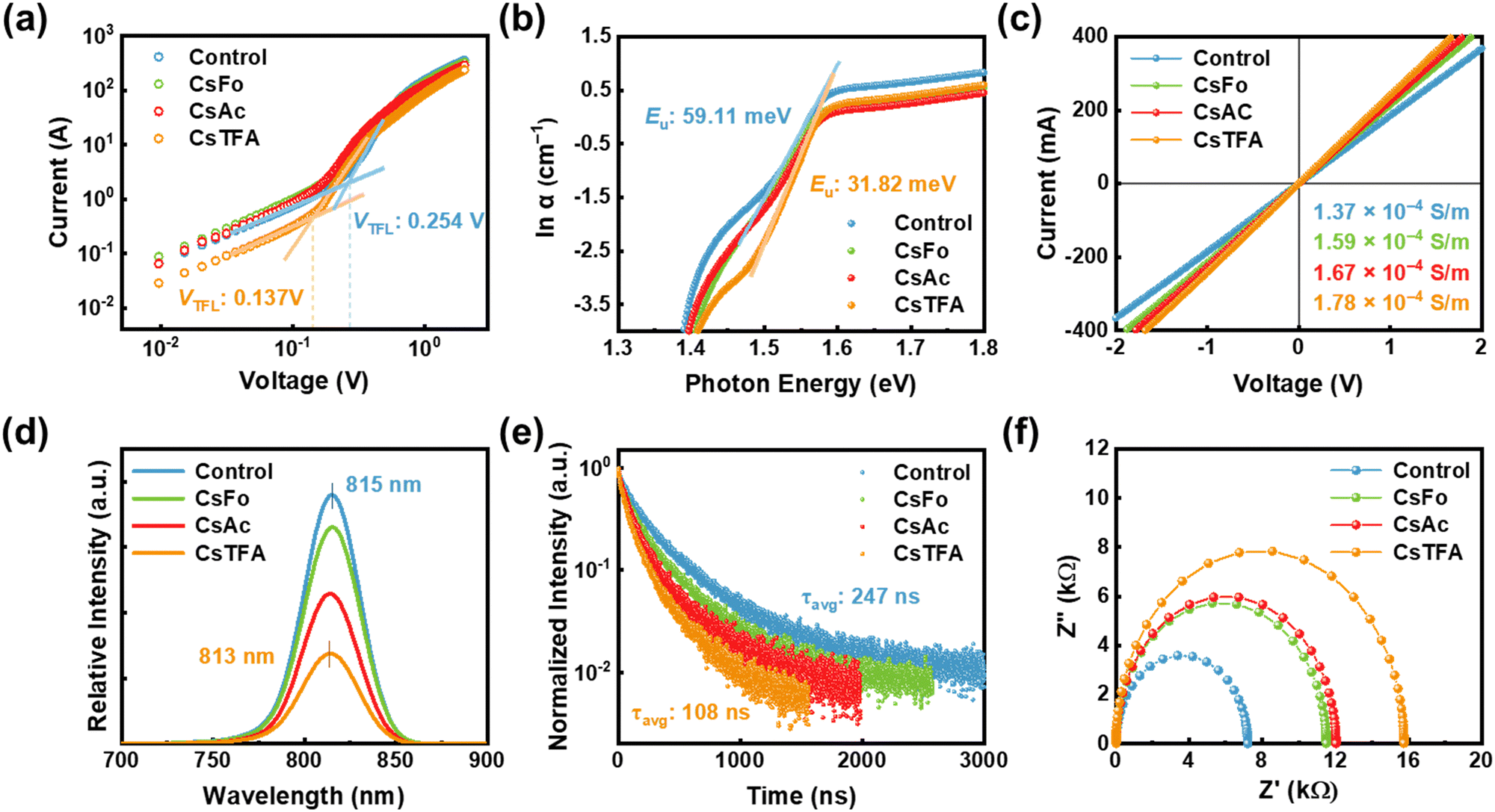 | ||
| Fig. 4 (a) SCLC curves for electron-only devices with a configuration of ITO/SnO2/Perovskite/PCBM/Au. (b) Urbach energy (Eu) of the perovskite films deposited on the control- and CsX-treated SnO2. (c) J–V curves of the devices with the structure FTO/control- and CsX-treated SnO2/Au. (d) Steady-state PL spectra and (e) TRPL curves of the perovskite films deposited on the control- and CsX-treated SnO2. (f) Nyquist plots of the devices using the control- and CsX-treated SnO2. | ||
We performed steady-state PL and time-resolved PL (TRPL) measurements for the perovskite films deposited on the ETL substrates, aiming to confirm the efficient electron transporting behaviour between the SnO2 ETL and perovskite. A notably diminished PL intensity, coupled with a slight blue shift from 815 to 813 nm, is noted for the perovskite films deposited on the CsTFA-treated SnO2, compared to that on the control-SnO2, which suggests the efficient charge separation at the interface between the SnO2 and perovskite (Fig. 4d and Table S3, ESI†). As shown in Fig. 4e, such efficient electron extraction at the interface is also evidenced by the shortened PL decay for the perovskite films deposited on the CsTFA-treated SnO2 ETL. Combining the two results suggests that CsTFA treatment on the SnO2 also effectively reduces the non-radiative recombination pathways at the heterointerface. Although PL decay could be shortened due to interfacial defects, this effect is negligible as CsX treatment has reduced these defects. To obtain further insight into the interfacial electron transport/recombination behaviour, we performed electrochemical impedance spectroscopy (EIS) measurements (Fig. 4f). As summarized in Fig. S22 (ESI†), devices employing the CsTFA-treated SnO2 ETL manifest an augmented recombination resistance (Rrec, from 7.21 kΩ to 15.75 kΩ) and a decreased series resistance (Rs, from 14.16 Ω to 12.69 Ω), in comparison to those utilizing the control-SnO2 ETL. These results corroborate the aforementioned lower trap state density and higher conductivity of the CsTFA-treated SnO2 ETL. Additionally, ultraviolet photoelectron spectroscopy (UPS) measurements were conducted to evaluate the modified energy alignment of the SnO2 with adjoining perovskite films following CsX treatment (Fig. S23 and S24, ESI†). As a result of CsTFA treatment on SnO2, the lowest unoccupied molecular orbitals shift from −4.22 eV (for control-SnO2) to −4.11 eV, thereby decreasing the band offset between the SnO2 ETL and perovskite from 0.12 eV to 0.01 eV. Consequently, the reduced difference in band offset between the CsTFA-treated SnO2 ETL and perovskite further enhances the efficient extraction of electrons from the perovskite layer, which contributes to the improvement of VOC and fill factor (FF).57
We assessed the performance of PSCs with a structure of FTO/c-TiO2/control-SnO2 and CsX-treated SnO2/perovskite/Spiro-OMeTAD/Au (Fig. 5a). PSCs using control- and CsX-treated SnO2 ETL are denoted as control- and CsX-PSCs, respectively. The optimized concentration of CsX is 1 mg mL−1, achieving 25.13%, 25.46%, and 25.60% (certified at 25.39%) of champion PCEs in CsFo, CsAc, and CsTFA-PSCs, respectively, compared to 23.77% of control-PSCs (Fig. 5b and Fig. S25 and S26, ESI†). In particular, it is worth noting that the synergetic effects of bidirectional coordination subsequent to CsTFA treatment result in a substantial enhancement across all photovoltaic parameters including the open circuit voltage (VOC), short circuit current density (JSC), and FF (Table S4, ESI†). The integrated current density obtained from the external quantum efficiency (EQE) spectra is consistent with the JSC values measured under 1-sun (100 mW cm−2) illumination (Fig. 5c). In terms of efficiency, they also display remarkable reliability under all conditions (Fig. 5d). We measured J–V curves in both forward and reverse scanning directions to assess the hysteresis in PSCs (Fig. S27, ESI†). The control-PSCs demonstrate PCEs of 23.22% and 21.66% in the reverse and forward scanning directions, respectively, with a hysteresis index (HI) of 0.067. In contrast, the CsTFA-PSCs exhibit reduced dependence of PCEs on scanning directions (25.38% and 24.98% in the reverse and forward scanning directions, respectively), evident in a lower HI of 0.015 (Table S5, ESI†).
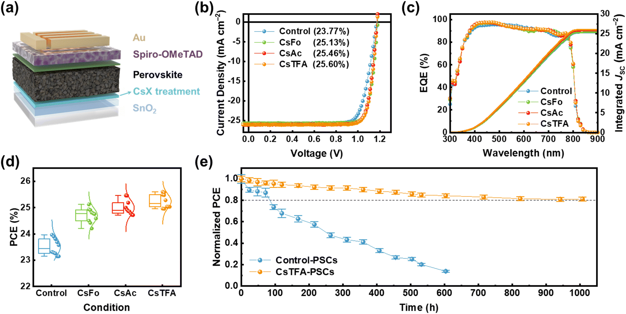 | ||
| Fig. 5 (a) The configuration of a typical FAPbI3 PSC device. (b) J–V curves of the control- and CsX-PSCs under reverse voltage scans. (c) EQE and the integrated JSC of the control and CsX-PSCs. (d) Statistic distribution of PCE of the PSCs with an optimized concentration of CsX. (e) The light-soaking stability of the PSCs under prolonged light exposure under ambient conditions (25 °C, 25% RH). | ||
To substantiate the enhancement of photovoltaic parameters, we examine the dependence of the JSC and VOC, illustrating the carrier recombination mechanism, across a range of incident light intensities ranging from 1.5 to 100 mW cm−2 (Fig. S28, ESI†). The JSC values are plotted against the natural logarithmic light intensity (JSC ∝ Iα). The α value for the control-PSCs is 0.956, whereas for the CsTFA-PSCs, it is determined to be 0.990, denoting the suppressed bimolecular recombination of charge carriers in the CsTFA-PSCs (Fig. S28a, ESI†).58 It also suggests that the increased transfer of photogenerated charge carriers into the CsTFA-treated SnO2 ETL contributes to the increased JSC observed in the CsTFA-PSCs. Furthermore, the ideality factor (nid), derived from the slope of VOC–light intensity curves (Fig. S28b, ESI†), is found to be 1.300 for the control-PSCs. Conversely, the CsTFA-PSCs exhibit a diminished value of 1.117, signifying effective mitigation of non-radiative recombination losses within the device upon treatment of CsTFA.49 The improvement of VOC and FF can be ascribed to the advantageous charge extraction/transportation behaviours, alongside the attenuation of non-radiative recombination. We measured the built-in potential (Vbi) by analysing the Mott–Schottky curves (Fig. S29, ESI†). The higher Vbi value ensures the facile extraction of photogenerated charge carriers within the device, facilitated by the built-in electric field. Hence, further evidence of the enhanced VOC in the CsTFA-PSCs is demonstrated by the elevated Vbi value of 1.13 V observed in the CsTFA-PSCs, contrasting with the 1.06 V recorded for the control-PSCs.
During light exposure, the excess or residual PbI2 present at the buried interface readily undergoes photodecomposition into metallic (Pb0) and iodine (I2), thereby resulting in the compromised long-term stability of PSCs under light soaking conditions.8,59,60 The presence of the residual PbI2, identified by its bright flaky structure, is evident on the underside of the control perovskite film, as revealed in the SEM images (Fig. S30, ESI†). Thus, we conducted an assessment of long-term stability under light illumination to discern the impact of CsTFA treatment on the stability of the PSCs (Fig. 5e). This measurement was conducted under ambient conditions without encapsulation. A rapid decline in PCEs of 73.6% is observed for the control-PSCs after only 100 hours of prolonged light exposure. In contrast, the CsTFA-PSCs maintained over 80% of their initial PCEs after 1000 hours. As evidenced by the XPS results, extended light exposure caused severe photodecomposition in the control-PSCs, attributed to residual PbI2 (Fig. S31, ESI†), thereby exacerbating their light soaking stability. Consequently, the robust perovskite film deposited on the CsTFA-treated SnO2 substrate, characterized by its monolithic grains, absence of strain, and a benign buried interface, ensures a boost in light soaking stability as well as photovoltaic performance.
Conclusions
In summary, we have proposed an advanced bidirectional coordination strategy entailing the deposition of CsTFA onto the SnO2 surface. The dual functionality of the TFA− anion molecule fosters interactions with both the SnO2 substrate and the perovskite lattice, thereby not only promoting orderly crystal initiation with a favourable growth orientation but also supporting their vertical growth. The well-developed three-dimensional perovskite crystal manifests as devoid of residual lattice strain and exhibiting fewer crystalline defects. Moreover, in parallel, a benign buried interface prevents non-radiative recombination losses at the interface, ensuring higher VOC and FF values in the PSCs. As a result, this synergy of advantages yielded a peak PCE of 25.60%, showcasing sustained resilience even under prolonged light exposure after 1000 hours. This groundbreaking bidirectional coordination strategy reveals a promising pathway to enhance high efficiency and confront the persistent challenge of addressing long-term stability concerns.Author contributions
Y. S. S., J. L., and D. S. K. conceived the idea and designed the experiments. G. L., J. Y. K., and D. S. K. supervised the work. Y. S. S., J. L., E. O., G. L., and D. S. K. wrote the manuscript. Y. S. S. and J. L. carried out the device fabrication and characterization studies. E. O. and G. L. carried out the DFT calculations and data analysis. J. S. carried out GIXRD and rocking curve measurements. J. R. carried out XPS and UPS measurements. D. L. conducted an analysis of the electrical properties of SnO2 and the perovskite. Y. L. carried out AFM measurements. T. S. carried out SEM measurements. H. J. and J. W. S. carried out perovskite film characterization studies. All authors discussed the results and contributed to the final manuscript.Data availability
The data supporting this article have been included as part of the ESI.†Conflicts of interest
There are no conflicts to declare.Acknowledgements
This work was supported by the National Research Foundation of Korea (NRF) grant funded by the Korean government (MSIT) (NRF-2018R1A5A1025594, RS-2023-00257666, and NRF-2023R1A2C3007358). This work was supported by the Technology Development Program to Solve Climate Changes of the NRF funded by the Ministry of Science, ICT (2020M1A2A2080746). G. L. acknowledges the support of computational resources from the National Supercomputing Center, KISTI (KSC-2024-CRE-0201).Notes and references
- Z. Liang, Y. Zhang, H. Xu, W. Chen, B. Liu, J. Zhang, H. Zhang, Z. Wang, D.-H. Kang, J. Zeng, X. Gao, Q. Wang, H. Hu, H. Zhou, X. Cai, X. Tian, P. Reiss, B. Xu, T. Kirchartz, Z. Xiao, S. Dai, N.-G. Park, J. Ye and X. Pan, Nature, 2023, 624, 557–563 CrossRef CAS PubMed
.
- H. Chen, C. Liu, J. Xu, A. Maxwell, W. Zhou, Y. Yang, Q. Zhou, A. S. R. Bati, H. Wan, Z. Wang, L. Zeng, J. Wang, P. Serles, Y. Liu, S. Teale, Y. Liu, M. I. Saidaminov, M. Li, N. Rolston, S. Hoogland, T. Filleter, M. G. Kanatzidis, B. Chen, Z. Ning and E. H. Sargent, Science, 2024, 384, 189–193 CrossRef CAS PubMed
- Z. Huang, Y. Bai, X. Huang, J. Li, Y. Wu, Y. Chen, K. Li, X. Niu, N. Li, G. Liu, Y. Zhang, H. Zai, Q. Chen, T. Lei, L. Wang and H. Zhou, Nature, 2023, 623, 531–537 CrossRef CAS PubMed
- Q. Jiang, J. Tong, Y. Xian, R. A. Kerner, S. P. Dunfield, C. Xiao, R. A. Scheidt, D. Kuciauskas, X. Wang, M. P. Hautzinger, R. Tirawat, M. C. Beard, D. P. Fenning, J. J. Berry, B. W. Larson, Y. Yan and K. Zhu, Nature, 2022, 611, 278–283 CrossRef CAS PubMed
- C. Liu, Y. Yang, H. Chen, J. Xu, A. Liu, A. S. R. Bati, H. Zhu, L. Grater, S. S. Hadke, C. Huang, V. K. Sangwan, T. Cai, D. Shin, L. X. Chen, M. C. Hersam, C. A. Mirkin, B. Chen, M. G. Kanatzidis and E. H. Sargent, Science, 2023, 382, 810–815 CrossRef CAS PubMed
- Q. Jiang, Y. Zhao, X. Zhang, X. Yang, Y. Chen, Z. Chu, Q. Ye, X. Li, Z. Yin and J. You, Nat. Photonics, 2019, 13, 460–466 CrossRef CAS
- J. Park, J. Kim, H.-S. Yun, M. J. Paik, E. Noh, H. J. Mun, M. G. Kim, T. J. Shin and S. I. Seok, Nature, 2023, 616, 724–730 CrossRef CAS PubMed
- C. Luo, G. Zheng, F. Gao, X. Wang, C. Zhan, X. Gao and Q. Zhao, Nat. Photonics, 2023, 17, 856–864 CrossRef CAS
- Y. Gao, F. Ren, D. Sun, S. Li, G. Zheng, J. Wang, H. Raza, R. Chen, H. Wang, S. Liu, P. Yu, X. Meng, J. He, J. Zhou, X. Hu, Z. Zhang, L. Qiu, W. Chen and Z. Liu, Energy Environ. Sci., 2023, 16, 2295–2303 RSC
- X. Yang, D. Luo, Y. Xiang, L. Zhao, M. Anaya, Y. Shen, J. Wu, W. Yang, Y.-H. Chiang, Y. Tu, R. Su, Q. Hu, H. Yu, G. Shao, W. Huang, T. P. Russell, Q. Gong, S. D. Stranks, W. Zhang and R. Zhu, Adv. Mater., 2021, 33, 2006435 CrossRef CAS PubMed
- W. Meng, K. Zhang, A. Osvet, J. Zhang, W. Gruber, K. Forberich, B. Meyer, W. Heiss, T. Unruh, N. Li and C. J. Brabec, Joule, 2022, 6, 458–475 CrossRef CAS
- S. Chen, X. Dai, S. Xu, H. Jiao, L. Zhao and J. Huang, Science, 2021, 373, 902–907 CrossRef CAS PubMed
- I. Levine, A. Al-Ashouri, A. Musiienko, H. Hempel, A. Magomedov, A. Drevilkauskaite, V. Getautis, D. Menzel, K. Hinrichs, T. Unold, S. Albrecht and T. Dittrich, Joule, 2021, 5, 2915–2933 CrossRef CAS
- Y. Dong, W. Shen, W. Dong, C. Bai, J. Zhao, Y. Zhou, F. Huang, Y.-B. Cheng and J. Zhong, Adv. Energy Mater., 2022, 12, 2200417 CrossRef CAS
- M. Kim, J. Jeong, H. Lu, T. K. Lee, F. T. Eickemeyer, Y. Liu, I. W. Choi, S. J. Choi, Y. Jo, H.-B. Kim, S.-I. Mo, Y.-K. Kim, H. Lee, N. G. An, S. Cho, W. R. Tress, S. M. Zakeeruddin, A. Hagfeldt, J. Y. Kim, M. Grätzel and D. S. Kim, Science, 2022, 375, 302–306 CrossRef CAS PubMed
- Y. Wang, M. Han, R. Wang, J. Zhao, J. Zhang, H. Ren, G. Hou, Y. Ding, Y. Zhao and X. Zhang, J. Mater. Chem. A, 2023, 11, 8573–8598 RSC
- H. Gao, K. Xiao, R. Lin, S. Zhao, W. Wang, S. Dayneko, C. Duan, C. Ji, H. Sun, A. D. Bui, C. Liu, J. Wen, W. Kong, H. Luo, X. Zheng, Z. Liu, H. Nguyen, J. Xie, L. Li, M. I. Saidaminov and H. Tan, Science, 2024, 383, 855–859 CrossRef CAS PubMed
- D.-J. Xue, Y. Hou, S.-C. Liu, M. Wei, B. Chen, Z. Huang, Z. Li, B. Sun, A. H. Proppe, Y. Dong, M. I. Saidaminov, S. O. Kelley, J.-S. Hu and E. H. Sargent, Nat. Commun., 2020, 11, 1514 CrossRef CAS PubMed
- N. Rolston, K. A. Bush, A. D. Printz, A. Gold-Parker, Y. Ding, M. F. Toney, M. D. McGehee and R. H. Dauskardt, Adv. Energy Mater., 2018, 8, 1802139 CrossRef
- Y. Chen, Y. Lei, Y. Li, Y. Yu, J. Cai, M.-H. Chiu, R. Rao, Y. Gu, C. Wang, W. Choi, H. Hu, C. Wang, Y. Li, J. Song, J. Zhang, B. Qi, M. Lin, Z. Zhang, A. E. Islam, B. Maruyama, S. Dayeh, L.-J. Li, K. Yang, Y.-H. Lo and S. Xu, Nature, 2020, 577, 209–215 CrossRef CAS PubMed
- C. Zhu, X. Niu, Y. Fu, N. Li, C. Hu, Y. Chen, X. He, G. Na, P. Liu, H. Zai, Y. Ge, Y. Lu, X. Ke, Y. Bai, S. Yang, P. Chen, Y. Li, M. Sui, L. Zhang, H. Zhou and Q. Chen, Nat. Commun., 2019, 10, 815 CrossRef CAS PubMed
- H.-S. Kim and N.-G. Park, NPG Asia Mater., 2020, 12, 78 CrossRef CAS
- X. Wang, H. Huang, M. Wang, Z. Lan, P. Cui, S. Du, Y. Yang, L. Yan, Q. Zhang, S. Qu and M. Li, Adv. Mater., 2024, 2310710 CrossRef CAS PubMed
- Y. Chen, Q. Wang, W. Tang, W. Qiu, Y. Wu and Q. Peng, Nano Energy, 2023, 107, 108154 CrossRef CAS
- C. Xu, S. Zhang, W. Fan, F. Cheng, H. Sun, Z. Kang and Y. Zhang, Adv. Mater., 2023, 35, 2207172 CrossRef CAS PubMed
- Y. Lin, Y. Liu, S. Chen, S. Wang, Z. Ni, C. H. Van Brackle, S. Yang, J. Zhao, Z. Yu, X. Dai, Q. Wang, Y. Deng and J. Huang, Energy Environ. Sci., 2021, 14, 1563–1572 RSC
- S. Chen, Y. Liu, X. Xiao, Z. Yu, Y. Deng, X. Dai, Z. Ni and J. Huang, Joule, 2020, 4, 2661–2674 CrossRef CAS
- Y. Jiang, J. Wang, H. Zai, D. Ni, J. Wang, P. Xue, N. Li, B. Jia, H. Lu, Y. Zhang, F. Wang, Z. Guo, Z. Bi, H. Xie, Q. Wang, W. Ma, Y. Tu, H. Zhou and X. Zhan, J. Am. Chem. Soc., 2022, 144, 5400–5410 CrossRef CAS PubMed
- C.-M. Hung, C.-L. Mai, C.-C. Wu, B.-H. Chen, C.-H. Lu, C.-C. Chu, M.-C. Wang, S.-D. Yang, H.-C. Chen, C.-Y. Yeh and P.-T. Chou, Angew. Chem., Int. Ed., 2023, 62, e202309831 CrossRef CAS PubMed
- F. Qiu, J. Sun, H. Liu and J. Qi, Chem. Eng. J., 2022, 446, 136936 CrossRef CAS
- C. Wu, L. Zhu, Y. Zhang and J. Dai, J. Electron. Mater., 2020, 49, 7144–7152 CrossRef
- J. Xi, J. Yuan, J. Du, X. Yan and J. Tian, Small, 2022, 18, 2203519 CrossRef CAS PubMed
- J. Jeong, M. Kim, J. Seo, H. Lu, P. Ahlawat, A. Mishra, Y. Yang, M. A. Hope, F. T. Eickemeyer, M. Kim, Y. J. Yoon, I. W. Choi, B. P. Darwich, S. J. Choi, Y. Jo, J. H. Lee, B. Walker, S. M. Zakeeruddin, L. Emsley, U. Rothlisberger, A. Hagfeldt, D. S. Kim, M. Grätzel and J. Y. Kim, Nature, 2021, 592, 381–385 CrossRef CAS PubMed
- Y. Zhu, Z. Zhang, X. Zhao, M. Li, Y. Feng, S. Zhang, W. Gao, J. Chen, J.-X. Tang and C. Chen, Adv. Energy Mater., 2024, 14, 2303946 CrossRef CAS
- M. Hossain, R. Garai, R. K. Gupta, R. N. Arunagirinathan and P. K. Iyer, J. Mater. Chem. C, 2021, 9, 10406–10413 RSC
- N. Wei, Y. Chen, X. Wang, Y. Miao, Z. Qin, X. Liu, H. Wei and Y. Zhao, Adv. Funct. Mater., 2022, 32, 2108944 CrossRef CAS
- M. Saliba, T. Matshu, J.-Y. Seo, K. Domanski, J.-P. Correa-Baena, M. K. Nazeeruddin, S. M. Zakeeruddin, W. Tress, A. Abate, A. Hagfeldt and M. Grätzel, Energy Environ. Sci., 2016, 9, 1989–1997 RSC
- Z. Li, M. Yang, J.-S. Park, S.-H. Wei, J. J. Berry and K. Zhu, Chem. Mater., 2016, 28, 284–292 CrossRef CAS
- T. Niu, F. Zhen, Y.-M. Xie, T. Yang, Q. Yao, J. Lu, K. Zhao and H.-L. Yip, ACS Appl. Mater. Interfaces, 2022, 14, 52838–52848 CrossRef CAS PubMed
- X. Ji, L. Bi, Q. Fu, B. Li, J. Wang, S. Y. Jeong, K. Feng, S. Ma, Q. Liao, F. R. Lin, H. Y. Woo, L. Lu, A. K. Y. Jen and X. Guo, Adv. Mater., 2023, 35, 2303665 CrossRef CAS PubMed
- C. Zheng, L. Liu, Y. Li, A. Gao, Z. Yang, L. Zhang, Z. Liu, D. Wang and S. Liu, Adv. Energy Mater., 2023, 13, 2301302 CrossRef CAS
- P. Wang, J. Liu, W. Shang, T. Xu, M. Wang, Y. Shi, R. Cai and J. Bian, J. Phys. Chem. Lett., 2023, 14, 653–662 CrossRef CAS PubMed
- W. Shao, H. Wang, F. Ye, C. Wang, C. Liu, S. Zhou, C. Tao and G. Fang, J. Power Sources, 2022, 520, 230900 CrossRef CAS
- D. Liu, Z. Shao, J. Gui, M. Chen, M. Liu, G. Cui, S. Pang and Y. Zhou, Chem. Commun., 2019, 55, 11059–11062 RSC
- S. Bi, H. Wang, J. Zhou, S. You, Y. Zhang, X. Shi, Z. Tang and H. Zhou, J. Mater. Chem. A, 2019, 7, 6840–6848 RSC
- X. Zhang, D. Zhang, Y. Zhou, Y. Du, J. Jin, Z. Zhu, Z. Wang, X. Cui, J. Li, S. Wu, J. Zhang and Q. Tai, Adv. Funct. Mater., 2022, 32, 2205478 CrossRef CAS
- C. Bi, Q. Wang, Y. Shao, Y. Yuan, Z. Xiao and J. Huang, Nat. Commun., 2015, 6, 7747 CrossRef CAS PubMed
- N. Wei, Y. Miao, X. Wang, Z. Qin, X. Liu, H. Chen, H. Wang, Y. Liang, S. Wang, Y. Zhao and Y. Chen, JACS Au, 2023, 3, 3324–3332 CrossRef CAS PubMed
- L. Deng, H. Wang, S. Rafique, Y. Wang, T. Hu, K. Liu, Y. Wang, X. Li, Z. Xie, J. Tang, Z. Liu, J. Li, W. Yuan, J. Wang, A. Yu and Y. Zhan, Adv. Funct. Mater., 2023, 33, 2303742 CrossRef CAS
- C. Luo, G. Zheng, F. Gao, X. Wang, Y. Zhao, X. Gao and Q. Zhao, Joule, 2022, 6, 240–257 CrossRef CAS
- Z. Wang, Q. Lin, F. P. Chmiel, N. Sakai, L. M. Herz and H. J. Snaith, Nat. Energy, 2017, 2, 17135 CrossRef CAS
- G. Kresse and J. Furthmüller, Comput. Mater. Sci., 1996, 6, 15–50 CrossRef CAS
- H. Zhang, Z. Chen, M. Qin, Z. Ren, K. Liu, J. Huang, D. Shen, Z. Wu, Y. Zhang, J. Hao, C.-s Lee, X. Lu, Z. Zheng, W. Yu and G. Li, Adv. Mater., 2021, 33, 2008487 CrossRef CAS PubMed
- Y. Zhang, P. Wang, X. Yu, J. Xie, X. Sun, H. Wang, J. Huang, L. Xu, C. Cui, M. Lei and D. Yang, J. Mater. Chem. A, 2016, 4, 18509–18515 RSC
- Z. Xiong, X. Chen, B. Zhang, G. O. Odunmbaku, Z. Ou, B. Guo, K. Yang, Z. Kan, S. Lu, S. Chen, N. A. N. Ouedraogo, Y. Cho, C. Yang, J. Chen and K. Sun, Adv. Mater., 2022, 34, 2106118 CrossRef CAS PubMed
- X. Zhang, D. Zhang, T. Guo, J. Zou, J. Jin, C. Zheng, Y. Zhou, Z. Zhu, Z. Hu, Q. Cao, S. Wu, J. Zhang and Q. Tai, J. Mater. Chem. A, 2023, 11, 9616–9625 RSC
- Z. Guo, A. K. Jena, G. M. Kim and T. Miyasaka, Energy Environ. Sci., 2022, 15, 3171–3222 RSC
- Y. Su, J. Yang, G. Liu, W. Sheng, J. Zhang, Y. Zhong, L. Tan and Y. Chen, Adv. Funct. Mater., 2022, 32, 2109631 CrossRef CAS
- J. Liang, X. Hu, C. Wang, C. Liang, C. Chen, M. Xiao, J. Li, C. Tao, G. Xing, R. Yu, W. Ke and G. Fang, Joule, 2022, 6, 816–833 CrossRef CAS
- G. Tumen-Ulzii, C. Qin, D. Klotz, M. R. Leyden, P. Wang, M. Auffray, T. Fujihara, T. Matsushima, J.-W. Lee, S.-J. Lee, Y. Yang and C. Adachi, Adv. Mater., 2020, 32, 1905035 CrossRef CAS PubMed
Footnotes |
| † Electronic supplementary information (ESI) available. See DOI: https://doi.org/10.1039/d4ee02017k |
| ‡ These authors equally contributed to this work. |
| This journal is © The Royal Society of Chemistry 2024 |