
Au nanoparticle decorated WO3 photoelectrode for enhanced photoelectrochemical properties†
Fang Xu*,
Yanwen Yao,
Dandan Bai,
Ruishu Xu,
Jingjing Mei,
Dapeng Wu,
Zhiyong Gao and
Kai Jiang*
Collaborative Innovation Center of Henan Province for Green Manufacturing of Fine Chemicals, Key Laboratory of Green Chemical Media and Reactions, Ministry of Education, School of Chemistry and Chemical Engineering, Henan Normal University, Xinxiang, Henan 453007, P. R. China. E-mail: jiangkai6898@126.com; Fax: +86 3733326209
First published on 1st July 2015
Abstract
An Au decorated WO3 photoelectrode was successfully synthesized and the photoelectrochemical properties were studied. Due to the enhanced light absorption, higher carrier density and lower transport resistance resulting from the surface plasmon resonance of Au nanoparticles, an improved photocurrent density of 0.44 mA cm−2 at 1 V vs. Ag/AgCl in 0.5 M NaSO4 under irradiation of 100 mW cm−2 was achieved, demonstrating about quadruple than that of a WO3 photoelectrode.
Given the tremendous impact on political, social and economic life, the steadily growing energy crisis and environmental problems have directed a global trend towards sustainable development. Solar induced water splitting has been regarded as one of the most attractive routes in view of the abundant and renewable nature of solar and water resources.1–3 Ever since water splitting into hydrogen and oxygen by a TiO2 photoelectrode under ultraviolet illumination was reported by Fujishima and Honda,4 photoelectrochemical (PEC) cells are widely used as water splitting devices. Many efforts have been made to develop photoanodes to improve solar-to-hydrogen conversion efficiency. Among various photoanode materials, WO3 has attracted extensive attentions due to the highly positive valence band edge (∼2.6 eV vs. NHE), which can provide a large driving force for photogenerated holes to oxidize water.5–9 However, there are three main factors that prevent WO3 from being a highly efficient and durable photoanode material for oxygen evolution reaction (OER). Firstly, WO3 has a band gap of ∼2.6 eV, which prevents WO3 from absorbing the vast proportion of visible light in the solar spectrum. Secondly, the hole diffusion length of WO3 is ∼150 nm; only the holes generated from an electrode surface can evolve into water splitting reactions. Thirdly, photocorrosion of WO3 in neutral and basic solutions greatly decreases the photoelectrochemical performance. In order to overcome the issues mentioned above, fruitful strategies have been developed. For example, doping, photosensitizing or forming heterojunctions has been used to improve WO3 photoelectrode activity. It has been reported that Fe2O3,10,11 BiVO4,12 CdS13, etc. have been combined with WO3 to expand the absorption band in the solar spectrum.14–17 Regretfully, these strategies can’t satisfy the requirements of the photoelectrode because the interface, surface and other defects can capture photogenerated carriers and deteriorate the activity of the photoelectrode.
Recently, metal nanostructures, such as Ag, Au, Cu, which possess strong absorptions in the visible spectrum due to localized surface plasmon resonance (SPR) effect, improved the apparent photoactivity of the semiconductor in the visible region.18–20 Moreover, noble metal nanoparticles have considerable photostability compared to semiconductor nanoparticles. Plasmonic Au has been suggested to sensitize photoelectrodes due to its high stability and excellent SPR effect. For example, the performances can be enhanced for Au nanoparticle deposited TiO2, ZnO, Fe2O3 photoelectrodes under solar illumination for PEC water splitting.21–23 The reason can be explained by the SPR induced electric field amplification near the oxide semiconductor surface, which increased the photon absorption rate of the photoanode and thus improved the photoactivity.24,25
Herein, we designed an Au decorated WO3 photoelectrode for water splitting (Experimental details, ESI†). WO3 nanoparticles were prepared via a hydrothermal method, and then were coated on a conducting glass substrate using a doctor blade method to prepare WO3 electrode. Au sol was prepared and dropped on the WO3 electrode. One drop-coating process was defined as one cycle, and a series of Au decorated WO3 films with 1, 5, 10, 15, 20 cycles were prepared; the samples were denoted as WO3–1Au, WO3–5Au, WO3–10Au, WO3–15Au, WO3–20Au respectively.
Fig. 1a displays the X-ray diffraction (XRD) patterns of Au nanoparticles, WO3 and WO3–Au films. For the XRD pattern of Au nanoparticles, the diffraction peaks are indexed to cubic Au (PDF no. 65-8601). The diffraction peaks in XRD patterns of WO3 film are indexed to the monoclinic phase of WO3 (JCPDS no. 05-0364) after subtracting diffraction peaks of FTO. The three characteristic diffraction peaks at 23.09, 23.51, 24.44 correspond to (002), (020), (200) peaks. For the XRD patterns of the WO3–Au films, the diffraction peak of Au at ∼38.2° can hardly be seen for WO3–1Au and WO3–5Au because of the low amount of Au. When the amount of Au increases, the diffraction peak appears and the intensity can be enhanced with the increment of Au amount. The results indicated the formation of the WO3–Au composite photoelectrode. Fig. 1b shows the UV-vis absorption spectra of the WO3 and WO3–Au photoelectrodes. A red shift of absorption edge and enhancement of light absorption for WO3–Au can be observed compared to WO3. In addition, the light absorption increases with the increment of Au in the visible range. Moreover, the absorption band centered at ∼550 nm enhances monotonically with the increase of Au content, which is corresponding to the SPR effect of Au nanoparticles, named plasmon resonance absorption.19,26 As a result, the incorporation of Au into the WO3 photoelectrode enhanced the light absorption due to the SPR effect of Au nanoparticles.
 | ||
| Fig. 1 (a) XRD patterns and (b) UV-vis absorption spectra of Au nanoparticles, WO3 and WO3–Au films. | ||
The morphology and composition of monoclinic WO3 and WO3–10Au are shown in Fig. 2. The FESEM image of the top view of the WO3 photoelectrode (Fig. 2a) suggests that a large number of cavities are dispersed on the surface of the photoelectrode. The cavities may be formed through the removal of organic matter in the paste during the annealing process. The high magnification FESEM image of the WO3 photoelectrode is shown in Fig. S1 (ESI†), and it can be seen that WO3 has rod-like nanoparticles. The EDS of WO3 (inset of Fig. 2a) indicates the composition of W and O elements, and the atom ratio of W and O is around 1![[thin space (1/6-em)]](https://www.rsc.org/images/entities/char_2009.gif) :3. The FESEM of WO3–10Au is shown in Fig. 2b and Au nanoparticles can hardly be observed due to the low amount and small size of Au nanoparticles. Fortunately, the existence of Au can be observed from the corresponding EDS shown in the inset. Moreover, from the EDS of WO3–10Au, the atom ratio of W and O is around 1:3; the quality percent of Au was around 1.2% as shown in Table S1 (ESI†). The elemental mapping of WO3–10Au (Fig. 2c) confirmed the existence of Au, W, and O elements. The results indicated the formation of the WO3–Au composite photoelectrode. The quality percent of Au for all the WO3–Au composites were shown in Table S2 (ESI†). The quality percent of WO3–1Au, WO3–5Au, WO3–10Au, WO3–15Au and WO3–20Au were 0.47 wt%, 0.65 wt%, 1.20 wt%, 1.40 wt% and 2.01 wt% respectively.
:3. The FESEM of WO3–10Au is shown in Fig. 2b and Au nanoparticles can hardly be observed due to the low amount and small size of Au nanoparticles. Fortunately, the existence of Au can be observed from the corresponding EDS shown in the inset. Moreover, from the EDS of WO3–10Au, the atom ratio of W and O is around 1:3; the quality percent of Au was around 1.2% as shown in Table S1 (ESI†). The elemental mapping of WO3–10Au (Fig. 2c) confirmed the existence of Au, W, and O elements. The results indicated the formation of the WO3–Au composite photoelectrode. The quality percent of Au for all the WO3–Au composites were shown in Table S2 (ESI†). The quality percent of WO3–1Au, WO3–5Au, WO3–10Au, WO3–15Au and WO3–20Au were 0.47 wt%, 0.65 wt%, 1.20 wt%, 1.40 wt% and 2.01 wt% respectively.
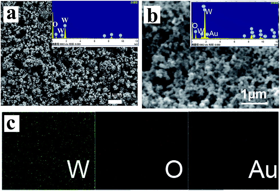 | ||
| Fig. 2 FESEM images of the top view of WO3 (a) and Au decorated WO3 (b) photoelectrodes; (c) elemental mapping of WO3–10Au. The insets of (a) and (b) are EDS of WO3 and Au decorated WO3 photoelectrodes respectively. | ||
The microstructure of WO3 and WO3–10Au was observed by TEM and HRTEM and the results are shown in Fig. 3. The TEM image shown in Fig. 3a reveals the rod-like WO3 nanoparticles; the length ranges from around 60 to 80 nm, and the width ranges from around 30 to 40 nm. In the HRTEM of an individual WO3 nanoparticle (Fig. 3c), the interplanar lattice spacing is ∼0.38 nm, which is consistent with the (002) plane of monoclinic phase WO3. Fig. 3b shows the TEM image of WO3–10Au; it can be observed that some small particles (marked in the circles) were dispersed on the surface of WO3 rod-like nanoparticles. As shown in the HRTEM of the WO3–10Au composite (Fig. 3d), the diameter of small particles on the surface of WO3 is around 10 nm and the lattice spacing is ∼0.23 nm, which is consistent with the (111) plane of Au. Moreover, the WO3 crystallites are highly ordered with a planar spacing observed of ∼0.38 nm, consistent with the (002) plane of monoclinic WO3.
 | ||
| Fig. 3 TEM images of WO3 nanoparticles (a) and Au decorated WO3 (b); high-resolution TEM images of WO3 nanoparticles (c) and Au decorated WO3 (d). | ||
To gain a better insight into the surface composition and chemical states of Au decorated WO3, we analyzed the WO3–10Au sample using XPS spectra (Fig. 4). As shown in the survey spectrum (Fig. 4a), the sample consists of W, O, Au and C, where the elemental C results from the carbon tape used in the XPS measurement. The survey spectra indicate the composition of the WO3–10Au sample. The high resolution XPS spectra for W 4f shown in Fig. 4b indicates the spin orbital splitting of the W 4f7/2 and W 4f5/2 core level of W6+ centered at ∼34.8 eV and ∼37 eV respectively, being assignable to WO3. Fig. 4c shows the O 1s spectrum. The intense peak centered at ∼529.8 eV can be assigned to the oxides of WO3, while the two weak peaks centered at ∼531.7 eV and ∼532.8 eV should be due to the adsorbed oxygen. Fig. 4d shows the Au 4f spectrum. The two peaks centered at ∼83.2 eV and ∼87 eV correspond to the binding energies of Au 4f7/2 and Au 4f5/2 for elemental Au0.
 | ||
| Fig. 4 XPS spectra of the WO3–10Au composite: (a) a survey scan, (b) W 4f, (c) O 1s and (d) Au 4f. | ||
The photoelectrochemical properties of the WO3 and WO3–Au photoanodes were studied in a three electrode cell using Ag/AgCl as reference electrode and Pt slice as counter electrode. Fig. 5a shows a set of linear sweep voltammograms (LSVs) of WO3 and WO3–Au photoelectrodes recorded in 0.5 M NaSO4 electrolyte under simulated solar irradiation (AM 1.5G, 100 mW cm−2) in the potential range between −0.2 V and 1.5 V vs. Ag/AgCl.
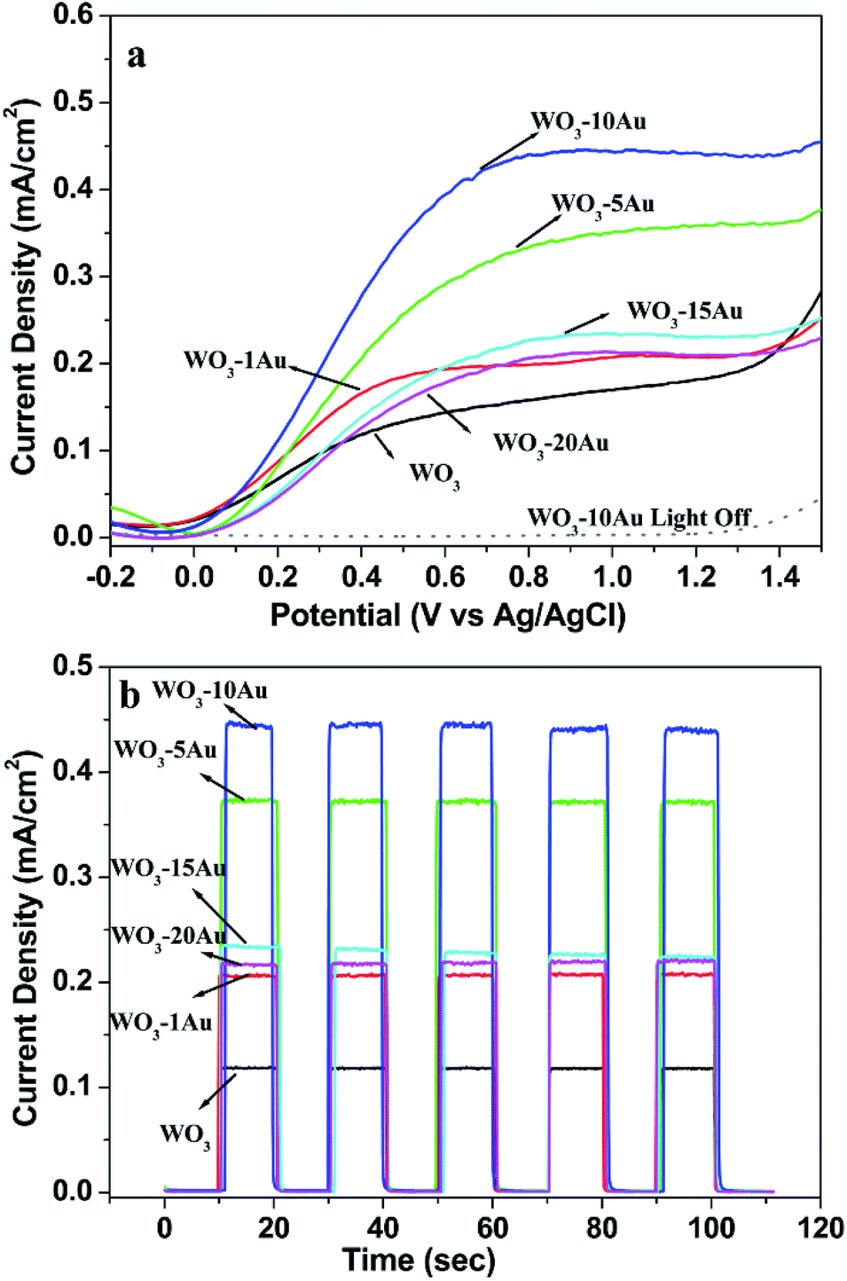 | ||
| Fig. 5 (a) Linear sweep voltammograms and (b) chronoamperomertic I–t curves collected at 1 V vs. Ag/AgCl of WO3 film and WO3–Au film electrodes recorded in 0.5 M aqueous Na2SO4 solution under simulated illumination (AM 1.5G, 100 mW cm−2). | ||
The current density of the WO3 electrode in the dark is very low and nearly can be neglected. Upon illumination, the WO3 photoelectrode and all of the WO3–Au photoelectrodes show pronounced photoresponse. In addition, the Au decorated WO3 photoelectrode exhibits a higher photocurrent than the WO3 photoelectrode. The results suggested that Au nanoparticles play important roles in enhancing the photocurrent density. The reason can be explained by the SPR effect of Au nanoparticles. Meanwhile, the SPR-induced electromagnetic field enhancement effects facilitated photogenerated electron and hole generation and separation.
It can also be found that the loading amount of Au has great influence on the photocurrent density. Specifically, the photocurrent density increases with the increment of Au from 1 cycle to 10 cycles and decreases when the Au amount increased to 15 and 20 cycles. Consequently, WO3–10Au achieved the highest photocurrent density of 0.44 mA cm−2 at 1 V (vs. Ag/AgCl), which was almost quadruple the photocurrent density of the bare WO3 (0.12 mA cm−2) photoanode obtained at the same potential. When the amount of Au NPs is low, the photocurrent increases with the increment of Au loading amount because the SPR effect enhances with the increment of Au amount. On the contrary, when the Au NP amount is high, the photocurrent density decreases, although they have higher absorption as shown in Fig. 1b. The reasons can be explained as follows: (1) the high coverage of Au NPs reduces the surface area of WO3 in direct contact with the electrolyte and thereby hinders the oxygen involved reaction; (2) the Au particles, with an increased amount on the WO3 surface, become recombination centers and increase the recombination of photogenerated electron and hole pairs due to the high concentration of grain boundaries, interface, point defects, etc. To examine the instant photoresponse of the electrodes, the chronoamperomertic I–t curves were collected under simulated solar illumination at 1 V vs. Ag/AgCl. As shown in Fig. 5b, the recorded photocurrent densities are consistent with the values obtained from the linear sweep voltammograms, indicating that the photocurrents are stable without photoinduced charging effect.
Electrochemical impedance spectroscopy (EIS) was commonly used to investigate the charge transfer resistance and the separation efficiency of photogenerated electrons and holes. To reveal the kinetics of charge transfer in the WO3–Au composite photoelectrode, the EIS measurement was carried out under illumination. Fig. 6a shows the Nyquist plots of the WO3 and WO3–Au photoanodes at a single constant potential (0 V vs. Ag/AgCl) with 10 mV potential perturbation amplitude and the frequency ranged from 10−1 Hz to 105 Hz in 0.5 M Na2SO4 electrolyte solution. Obviously, the resistance of WO3–Au photoelectrodes is smaller than that of the WO3 photoelectrode, and WO3–10Au has the smallest resistance. The results indicate that Au nanoparticles enhanced the electron mobility by suppressing the recombination of photogenerated electrons and holes in the WO3–Au composite photoanode. The reduced charge-transfer resistance is thought to be one key factor for enhancing the photoelectrochemical activities of the WO3–Au photoanode. The results can also be further confirmed by the corresponding Bode phase in Fig. S2 (ESI†).27 The maximum frequency and electron lifetimes (τ) of the WO3 and WO3–Au photoelectrodes have been calculated and were shown in Table 1. The WO3–10Au photoelectrode had the longest electron lifetime, which suggested the effective suppression of recombination of photogenerated electron–hole pairs during the electron transfer across the photoanode due to the SPR effect of Au nanoparticles.
 | ||
| Fig. 6 (a) Nyquist plots and (b) Mott–Schottky plots for the WO3 and WO3–Au photoelectrodes in 0.5 M Na2SO4 solution under AM 1.5-irradiation. | ||
| Samples | WO3 | WO3–1Au | WO3–5Au | WO3–10Au | WO3–15Au | WO3–20Au |
|---|---|---|---|---|---|---|
| fmax (Hz) | 122.1 | 97.66 | 68.13 | 46.42 | 56.23 | 97.66 |
| τ (ms) | 2.61 | 3.26 | 4.67 | 6.86 | 5.66 | 3.26 |
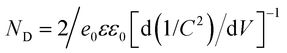
The capacitance was obtained at each potential with 1000 Hz frequency in the dark, and Mott–Schottky (MS) plots were generated from capacitance values. As shown in Fig. 6b, all the samples show positive slopes in the MS plots, indicating they are n-type semiconductors with electrons as majority carriers. The slopes determined from the MS curves were used to estimate the carrier density using the following equation:18
| Samples | WO3 | WO3–1Au | WO3–5Au | WO3–10Au | WO3–15Au | WO3–20Au |
|---|---|---|---|---|---|---|
| ND (1019 cm−3) | 5.85 | 6.49 | 8.74 | 12.7 | 8.66 | 8.27 |
To evaluate the photoelectrochemical efficiency of samples as a function of illumination wavelength, the IPCE measurements were conducted at a bias potential of 0.8 V vs. Ag/AgCl, and the results are shown in Fig. 7. The photoresponse of WO3–10Au is higher than that of the WO3 photoanode. The WO3–10Au photoanode exhibited maximum IPCE of approximately ∼12.7% at ∼330 nm, which is higher than that of the WO3 photoanode due to the SPR effect of Au nanoparticles.
 | ||
| Fig. 7 IPCE curves for WO3 and WO3–10Au. | ||
Based on above discussions, the electron-transfer mechanism of the Au decorated WO3 photoanode in PEC water splitting has been proposed in Scheme 1. Under the illumination, the electrons are excited from the valence band to the conduction band of WO3, leaving the same amount of holes in the valence band. The newly formed Fermi energy of the composite is lower than the energy level of the bottom of the conduction band of WO3, so the photoexcited electrons would be transferred from WO3 to Au, driven by the energy difference to reduce carrier recombination. Meanwhile, due to SPR excitation, Au nanoparticles absorb the resonant photons to generate hot electrons, and hot electrons were transferred to the conduction band of WO3. Finally, the leaving holes in the valence band of WO3 are immediately consumed to produce oxygen, and the electrons are injected into the Pt electrode via the conduction of WO3 to generated hydrogen.
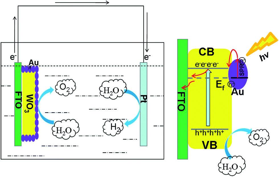 | ||
| Scheme 1 Schematics of the PEC cell and charge-separation process of the typical WO3–Au heterostructure photoanode. | ||
In this research, WO3–Au photoanodes were synthesized and used for photoelectrochemical water splitting. The optimized content of the Au decorated WO3 photoelectrode (WO3–10Au) achieved the maximum photocurrent density of 0.44 mA cm−2 at 1 V vs. Ag/AgCl in 0.5 M Na2SO4, which was almost four times than that of the WO3 photoelectrode under the same conditions. The enhancement of the WO3–10Au photoelectrochemical activity efficiency attributes to the surface plasmon resonance effect of Au nanoparticles which extended and enhanced the light absorption and enhanced the separation efficiency of the photogenerated electron–hole pairs.
Acknowledgements
This work is supported by National Natural Science Foundation of China (61204078, 61176004 and U1304505), Program for Innovative Research Team (in Science and Technology) in University of Henan Province (No. 13IRTSTHN026), Key Project of Science and Technology of Henan Province (No. 122102210561, 13A150517). Basic and Frontier Research Programs of Henan Province (No. 142300410420).Notes and references
- X. Liu, F. Wang and Q. Wang, Phys. Chem. Chem. Phys., 2012, 14, 7894–7911 RSC.
- H. M. Chen, C. K. Chen, R.-S. Liu, L. Zhang, J. Zhang and D. P. Wilkinson, Chem. Soc. Rev., 2012, 41, 5654–5671 RSC.
- F. E. Osterloh, Chem. Soc. Rev., 2013, 42, 2294–2320 RSC.
- A. Fujishima and H. Kenichi, Nature, 1972, 238, 37–38 CrossRef CAS PubMed.
- C. Ng, Y. H. Ng, A. Iwase and R. Amal, ACS Appl. Mater. Interfaces, 2013, 5, 5269–5275 CAS.
- P. M. Rao, L. Cai, C. Liu, I. S. Cho, C. H. Lee, J. M. Weisse, P. Yang and X. Zheng, Nano Lett., 2014, 14, 1099–1105 CrossRef CAS PubMed.
- M. Seifollahi Bazarjani, M. Hojamberdiev, K. Morita, G. Zhu, G. Cherkashinin, C. Fasel, T. Herrmann, H. Breitzke, A. Gurlo and R. Riedel, J. Am. Chem. Soc., 2013, 135, 4467–4475 CrossRef CAS PubMed.
- N. Wang, D. Wang, M. Li, J. Shi and C. Li, Nanoscale, 2014, 6, 2061–2066 RSC.
- J. Y. Zheng, G. Song, J. Hong, T. K. Van, A. U. Pawar, D. Y. Kim, C. W. Kim, Z. Haider and Y. S. Kang, Cryst. Growth Des., 2014, 14, 6057–6066 CAS.
- P. Zhao and B. E. Koel, ACS Appl. Mater. Interfaces, 2014, 6, 22289–22296 CAS.
- S. S. Shinde, R. A. Bansode, C. H. Bhosale and K. Y. Rajpure, J. Semicond., 2011, 32, 013001 CrossRef.
- S. Sun, W. Wang, D. Li, L. Zhang and D. Jiang, ACS Catal., 2014, 4, 3498–3503 CrossRef CAS.
- X. Zhang, Y. Li, J. Zhao, S. Wang, Y. Li, H. Dai and X. Sun, J. Power Sources, 2014, 269, 466–472 CrossRef CAS PubMed.
- J. Su, L. Guo, N. Bao and C. A. Grimes, Nano Lett., 2011, 11, 1928–1933 CrossRef CAS PubMed.
- K. Zhang, X. J. Shi, J. K. Kim and J. H. Park, Phys. Chem. Chem. Phys., 2012, 14, 11119–11124 RSC.
- S. Han, J. Li, X. Chen, Y. Huang, C. Liu, Y. Yang and W. Li, Int. J. Hydrogen Energy, 2012, 37, 16810–16816 CrossRef CAS PubMed.
- H. Li, Y. Zhou, L. Chen, W. Luo, Q. Xu, X. Wang, M. Xiao and Z. Zou, Nanoscale, 2013, 5, 11933–11939 RSC.
- J. Li, S. K. Cushing, P. Zheng, T. Senty, F. Meng, A. D. Bristow, A. Manivannan and N. Wu, J. Am. Chem. Soc., 2014, 136, 8438–8449 CrossRef CAS PubMed.
- Y. C. Pu, G. Wang, K. D. Chang, Y. Ling, Y. K. Lin, B. C. Fitzmorris, C. M. Liu, X. Lu, Y. Tong, J. Z. Zhang, Y. J. Hsu and Y. Li, Nano Lett., 2013, 13, 3817–3823 CrossRef CAS PubMed.
- T. Arai, M. Horiguchi, M. Yanagida, T. Gunji, H. Sugihara and K. Sayama, Chem. Commun., 2008, 5565–5567 RSC.
- J. Wang, S. Pan, M. Chen and D. A. Dixon, J. Phys. Chem. C, 2013, 117, 22060–22068 CAS.
- Y. G. Lin, Y. K. Hsu, Y. C. Chen, S. B. Wang, J. T. Miller, L. C. Chen and K. H. Chen, Energy Environ. Sci., 2015, 6, 8917–8922 Search PubMed.
- M. Wu, W. J. Chen, Y. H. Shen, F. Z. Huang, C. H. Li and S. K. Li, ACS Appl. Mater. Interfaces, 2014, 6, 15052–15060 CAS.
- X. Zhang, Y. Liu and Z. Kang, ACS Appl. Mater. Interfaces, 2014, 6, 4480–4489 CAS.
- K. A. Willets and R. P. van Duyne, Annu. Rev. Phys. Chem., 2007, 58, 267–297 CrossRef CAS PubMed.
- L. Liu, S. Ouyang and J. Ye, Angew. Chem., 2013, 125, 6821–6825 CrossRef PubMed.
- F. Xu, X. Zhang, Y. Wu, D. Wu, Z. Gao and K. Jiang, J. Alloys Compd., 2013, 574, 227–232 CrossRef CAS PubMed.
Footnote |
| † Electronic supplementary information (ESI) available: Experimental details, SEM of WO3 and Bode phase of samples. See DOI: 10.1039/c5ra06241a |
| This journal is © The Royal Society of Chemistry 2015 |