 Open Access Article
Highly (100)-oriented CH3NH3PbI3(Cl) perovskite solar cells prepared with NH4Cl using an air blow method†
Takeo Oku *,
Yuya Ohishi and
Naoki Ueoka
Department of Materials Science, The University of Shiga Prefecture, 2500 Hassaka, Hikone, Shiga 522-8533, Japan. E-mail: oku@mat.usp.ac.jp
First published on 15th March 2018
Abstract
The effects of adding NH4Cl via an air blow process on CH3NH3PbI3(Cl) perovskite solar cells were investigated. CH3NH3PbI3(Cl) solar cells containing various amounts of NH4Cl were fabricated by spin-coating. The microstructures of the resulting cells were investigated by X-ray diffraction, optical microscopy, and scanning electron microscopy. The current density–voltage characteristics of the cell were improved by adding an appropriate amount of NH4Cl and air blowing, which increased the photoconversion efficiency to 14%. Microstructure analysis indicated that the perovskite layer contained dense grains with strong (100) orientation, as a result of NH4Cl addition and air blowing. The ratio of the (100)/(210) reflection intensities for the perovskite crystals was 2000 times higher than that of randomly oriented grains. The devices were stable when stored in ambient air for two weeks.
Introduction
Thin film solar cells containing methylammonium trihalogenoplumbate(II) (CH3NH3PbI3) compounds with perovskite structures have recently been widely studied.1–4 This has been due to their easy fabrication processes and high photo-conversion efficiencies compared with conventional fullerene-based organic solar cells. Conversion efficiencies for these conventional cells have reached 15%,5 but higher efficiencies have been achieved for various perovskite compounds and device structures.6–8 Conversion efficiencies above 20% have been reported.9–18The photovoltaic properties of perovskite-based solar cells depend on the composition and crystal structure of the perovskite compound. Introducing metal atoms such as tin (Sn),19,20 antimony (Sb),21–25 copper (Cu),26 arsenic (As),27 germanium (Ge),28,29 indium (In),29 or thallium (Tl)29 at lead (Pb) sites has been performed. The optical absorption range of perovskite compounds has been extended by Sn or Tl doping.19,20,29
Introducing cesium,10 rubidium,14 formamidinium (NH![[double bond, length as m-dash]](https://www.rsc.org/images/entities/char_e001.gif) CHNH3, FA)12 or ethylammonium (CH3CH2NH3, EA)30 at methylammonium (CH3NH3, MA) sites can also improve conversion efficiencies. Studies on doping with bromine (Br)12,24 or chlorine (Cl)31,32 at iodine (I) sites of perovskite crystals have been reported. Doping with Cl reportedly increases the diffusion length, which improves the conversion efficiency.31,33 Various elemental and molecular dopants at Pb, I, and/or MA sites reportedly affect the photovoltaic properties and microstructures of perovskite-based solar cells.34
CHNH3, FA)12 or ethylammonium (CH3CH2NH3, EA)30 at methylammonium (CH3NH3, MA) sites can also improve conversion efficiencies. Studies on doping with bromine (Br)12,24 or chlorine (Cl)31,32 at iodine (I) sites of perovskite crystals have been reported. Doping with Cl reportedly increases the diffusion length, which improves the conversion efficiency.31,33 Various elemental and molecular dopants at Pb, I, and/or MA sites reportedly affect the photovoltaic properties and microstructures of perovskite-based solar cells.34
Photovoltaic properties also strongly depend on the morphology of thin films.35 A large interfacial area between the perovskite layers and TiO2 electron transport layers can increase carrier separation, which increases the short circuit current density. Smooth and homogeneous surfaces, interfaces, and grain boundary structures of perovskite layers are expected to result in improved open circuit voltages and fill factors.36
The present study investigates the effects of adding NH4Cl to perovskite CH3NH3PbI3(Cl) photovoltaic devices, using a hot air blow method. NH4Cl has surfactant properties, so is expected to promote a homogeneous morphology.37–39 The doped Cl is expected to increase the carrier diffusion length in the perovskite crystals.31,33 The Cl-doped perovskite crystals are denoted as CH3NH3PbI3(Cl) in the present study. The effects of NH4Cl addition on the formation of perovskite compounds for photovoltaic cells are investigated by light-induced current density–voltage (J–V) measurements, incident photon-to-current conversion efficiency (IPCE), X-ray diffraction (XRD), optical microscopy (OM), scanning electron microscopy (SEM), and energy dispersive X-ray spectroscopy (EDS).
Experimental
Materials
All reagents and solvents were used as received. For the compact TiO2 layer, 0.15 M and 0.30 M TiO2 precursor solutions were prepared from titanium diisopropoxide bis(acetylacetonate) (Sigma-Aldrich, 0.055 mL and 0.11 mL, respectively) with 1-butanol (1 mL). For the mesoporous TiO2 layer, TiO2 paste was prepared using TiO2 powder (Nippon Aerosil, P-25) with poly(ethylene glycol) (Nacalai Tesque, PEG #20000) in ultrapure water. The resulting dispersion was mixed with acetylacetone (Wako Pure Chemical Industries, 10 μL) and Triton X-100 (Sigma-Aldrich, 5 μL), stirred for 30 min, and then left to stand for 12 h to allow bubbles in the mixture to disperse.For the perovskite layer, a solution containing CH3NH3I (Showa Chemical Co., Ltd., 190.7 mg) and PbCl2 (Sigma-Aldrich, 111.2 mg) was prepared with a molar ratio of 3![[thin space (1/6-em)]](https://www.rsc.org/images/entities/char_2009.gif) :
:![[thin space (1/6-em)]](https://www.rsc.org/images/entities/char_2009.gif) 1 in N,N-dimethylformamide (Nacalai Tesque, 0.5 mL). This solution was then stirred at 60 °C for 24 h.
1 in N,N-dimethylformamide (Nacalai Tesque, 0.5 mL). This solution was then stirred at 60 °C for 24 h.
For the hole transport layer, two solutions of 2,2′,7,7′-tetrakis[N,N-di(p-methoxyphenyl)amino]-9,9′-spirobifluorene (spiro-OMeTAD, Sigma-Aldrich, 36.1 mg) in chlorobenzene (Wako Pure Chemical Industries, 0.5 mL) and lithium bis(trifluoromethylsulfonyl)imide (Li-TFSI, Tokyo Chemical Industry, 260 mg) in acetonitrile (Nacalai Tesque, 0.5 mL) were prepared and stirred for 12 h. The former spiro-OMeTAD solution in chlorobenzene containing 4-tert-butylpyridine (Aldrich, 14.4 μL) was mixed with the latter Li-TFSI solution (8.8 μL), and the resulting solution was stirred for 30 min at 70 °C.
Device fabrication
Fig. 1 shows a schematic illustration of the process used to fabricate the TiO2/CH3NH3PbI3(Cl) photovoltaic cells. Details of the basic fabrication process have been described previously,39–41 with the exception of details of the air blow procedure. F-doped tin oxide (FTO) substrates were ultrasonically cleaned with acetone and methanol, and then dried under nitrogen gas. The 0.15 M TiO2 precursor solution was spin-coated on the FTO substrate at 3000 rpm for 30 s, and the coated substrate was then heated to 125 °C for 5 min in air to form a TiOx layer.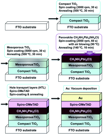 | ||
| Fig. 1 Schematic illustration of the process used to fabricate the CH3NH3PbI3(Cl) photovoltaic cells. | ||
The 0.30 M TiO2 precursor solution was spin-coated onto the TiOx layer at 3000 rpm for 30 s, and the coated substrate was then heated at 125 °C for 5 min. This process of coating with 0.30 M solution was performed a second time, and the resulting FTO substrate was then annealed at 500 °C for 30 min to form a compact TiO2 layer. For the mesoporous TiO2 layer, the TiO2 paste was spin-coated onto the substrate at 5000 rpm for 30 s. The substrate was then annealed at 120 °C for 5 min, and then at 500 °C for 30 min, to form a mesoporous TiO2 layer.
Then, a solution containing CH3NH3PbI3(Cl) was introduced into the TiO2 mesopores of the above coated substrate by the spin-coating method.42–44 For the spin-coating procedure, air blowing at a rate of 6 m s−1 and 3300 cm3 s−1 was applied perpendicular to the substrate at a temperature of 90 °C for 60 s, as indicated in Fig. 1. The resulting substrate was annealed at 140 °C for 10 min to form the perovskite layer.40
A hole transport layer was then prepared by spin-coating onto the perovskite layer. All procedures for preparing thin films were performed in ambient air at a temperature of 28 °C and humidity of ∼50%. Finally, a gold (Au) thin film was evaporated onto the hole transport layer, as the top metal electrode. The layered structure of the solar cell was denoted FTO/TiO2/CH3NH3PbI3(Cl)/spiro-OMeTAD/Au, as shown in Fig. 1.
Characterization
The J–V characteristics of the photovoltaic cells were measured under illumination at 100 mW cm−2, using an AM 1.5 solar simulator (San-ei Electric, XES-301S). J–V measurements were performed using a source measure unit (Keysight, B2901A Precision SMU). The scan rate and sampling time were ∼0.08 V s−1 and 1 m s, respectively. Four cells were tested for each cell composition. The solar cells were illuminated through the sides of the FTO substrates, and the illuminated area was 0.090 cm2. IPCE of the cells were also measured (Enli Technology, QE-R). The microstructures of the cells were investigated using an X-ray diffractometer (Bruker, D2 PHASER), a transmission optical microscope (Nikon, Eclipse E600), and a scanning electron microscope (Jeol, JSM-6010PLUS/LA) equipped with EDS.Results and discussion
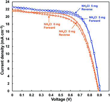
Fig. 2 shows the J–V characteristics of the TiO2/CH3NH3PbI3(Cl)/spiro-OMeTAD photovoltaic cells under illumination, in which the effects of NH4Cl addition are evident. Forward and reverse scans are indicated by the dotted and solid lines, respectively. The measured photovoltaic parameters of the TiO2/CH3NH3PbI3(Cl) cells are summarized in Table 1, and forward (Fw) and reverse (Rv) values are listed. Small hysteresis between the forward and reverse scans is observed for the J–V characteristics in Fig. 2, and the degree of hysteresis decreases with NH4Cl addition. A small amount of carriers may have been generated and transported into the TiO2 layer during the J–V measurements (i.e. during light irradiation and subsequent current flow). In this case, the electrical resistance would decrease and the photocurrent would increase, resulting in the hysteresis. The perovskite would also exhibit hysteresis properties in its J–V characteristics.45| NH4Cl (mg) | Scan | JSC (mA cm−2) | VOC (V) | FF | η (%) | ηave (%) | Rs (Ω cm−2) |
|---|---|---|---|---|---|---|---|
| 0 | Fw | 21.8 | 0.889 | 0.610 | 11.85 | 11.76 | 6.92 |
| Rv | 21.5 | 0.893 | 0.647 | 12.41 | 12.37 | 6.56 | |
| 1 | Fw | 22.4 | 0.909 | 0.633 | 12.90 | 12.50 | 6.44 |
| Rv | 22.2 | 0.912 | 0.651 | 13.19 | 12.89 | 6.18 | |
| 3 | Fw | 22.4 | 0.913 | 0.636 | 13.01 | 11.25 | 6.40 |
| Rv | 22.5 | 0.917 | 0.651 | 13.40 | 12.13 | 6.06 | |
| 5 | Fw | 22.6 | 0.908 | 0.673 | 13.83 | 13.59 | 4.66 |
| Rv | 22.6 | 0.908 | 0.685 | 14.03 | 13.74 | 4.70 |
The CH3NH3PbI3(Cl) cell without NH4Cl provides a power conversion efficiency (η) of 12.41% for the reverse scan. The average efficiency (ηave) of four electrodes in identical cells is 12.37%, as shown in Table 1. The short-circuit current density (JSC), open-circuit voltage (VOC) and fill factor (FF) are all higher for the NH4Cl-added CH3NH3PbI3(Cl) cells, which results in the increases in their η values. Adding 5 mg of NH4Cl yields the highest efficiency CH3NH3PbI3(Cl) cell, with a η of 14.03%, FF of 0.685, JSC of 22.6 mA cm−2, and VOC of 0.908 V. The highest average power conversion efficiency (ηave) of 13.74% is obtained for this cell. The series resistance (Rs) also decreases with NH4Cl addition (Table 1), leading to an increase in the JSC. After standing for two weeks in ambient air, the decreases in efficiencies of cells containing NH4Cl are small. A η of 13.19% is still obtained, as shown in Table 2.
| NH4Cl (mg) | JSC (mA cm−2) | VOC (V) | FF | η (%) | Rs (Ω cm−2) |
|---|---|---|---|---|---|
| 0 | 20.5 | 0.870 | 0.647 | 11.51 | 4.61 |
| 1 | 21.6 | 0.892 | 0.640 | 12.34 | 4.51 |
| 3 | 22.1 | 0.893 | 0.668 | 13.19 | 4.63 |
| 5 | 21.5 | 0.893 | 0.643 | 12.33 | 4.29 |
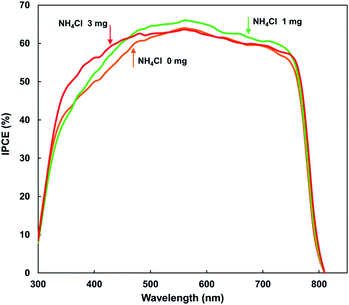
IPCE spectra of the CH3NH3PbI3(Cl) devices were shown in Fig. 3. The CH3NH3PbI3(Cl) cells show photoconversion efficiencies between 320 and 810 nm, which corresponds to an energy gap of 1.53 eV for the CH3NH3PbI3. The IPCE was improved in the range of 400–700 nm by adding NH4Cl, which lead to the increase of JSC values. Although the JSC values should agree with the integrated values of IPCE as previously reported in alkali metal-doped perovskite solar cells,46 the JSC values in the present work is slightly lower than the integrated values of IPCE. In order to measure the IPCE of the perovskite solar cells, DC measurements mode is better. However, the lowest frequency of the lock-in-amplifier in the present work is 4 Hz (QE-R, Enli Technology), and the lower IPCE values tended to be measured compared with the actual IPCE values. Therefore, only the wavelength region can be evaluated for the IPCE data in the present work.
OM images of the CH3NH3PbI3(Cl) cells are shown in Fig. 4. Microparticles with sizes of 5–10 μm are observed for the cell prepared without NH4Cl, as shown in Fig. 4(a). Adding NH4Cl to the CH3NH3PbI3(Cl) decreases the particle size, as shown in Fig. 4(b)–(d). In addition, networking structures with sizes of ∼10 μm between microparticles are observed, especially in Fig. 4(d). These networking microstructures could potentially improve the photovoltaic properties.
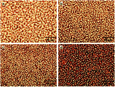 | ||
| Fig. 4 OM images of CH3NH3PbI3(Cl) cells containing (a) 0 mg, (b) 1 mg, (c) 3 mg, and (d) 5 mg of NH4Cl. | ||
A SEM image of the CH3NH3PbI3(Cl) cell without NH4Cl is shown in Fig. 5(a). Microparticles with sizes of 5–10 μm are observed on the surface of the mesoporous TiO2, which correspond to those in Fig. 4(a). The particles appear have crystal facets. EDS elemental mapping images of the Pb M line, I L line, Cl K line, C K line, and N K line are shown in Fig. 5(b)–(f), respectively. These elemental mapping images indicate that the particles observed in Fig. 5(a) correspond to the CH3NH3PbI3 compound. The Pb and I compositions and C![[thin space (1/6-em)]](https://www.rsc.org/images/entities/char_2009.gif) :
:![[thin space (1/6-em)]](https://www.rsc.org/images/entities/char_2009.gif) N ratio were calculated from the EDS spectrum using background correction by normalizing the peaks, and are listed in Table 3. Although the EDS values contain some errors, these results seem to indicate that the composition of CH3NH3PbI3 may be I deficient. In addition, EDS indicates that C is dispersed throughout the matrix.
N ratio were calculated from the EDS spectrum using background correction by normalizing the peaks, and are listed in Table 3. Although the EDS values contain some errors, these results seem to indicate that the composition of CH3NH3PbI3 may be I deficient. In addition, EDS indicates that C is dispersed throughout the matrix.
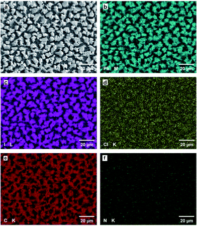 | ||
| Fig. 5 (a) SEM image of the CH3NH3PbI3(Cl) cell without NH4Cl, and corresponding elemental mapping images of the (b) Pb M line, (c) I L line, (d) Cl K line, (e) C K line, and (f) N K line. | ||
Fig. 6(a) shows a SEM image of the CH3NH3PbI3(Cl) cell containing 5 mg of NH4Cl. The surface morphology changes upon adding NH4Cl to the CH3NH3PbI3. The average particle sizes is ∼5 μm, and crystals are connected to each other with special facets. These networking surface structures could potentially improve the surface coverage and therefore the photovoltaic properties. Fig. 6(b)–(f) show EDS elemental mapping images of Pb, I, Cl, C, and N, respectively. The elemental compositions and C![[thin space (1/6-em)]](https://www.rsc.org/images/entities/char_2009.gif) :
:![[thin space (1/6-em)]](https://www.rsc.org/images/entities/char_2009.gif) N ratios were calculated from the EDS spectra, and are also listed in Table 3. These data indicate that the CH3NH3PbI3 starting composition may be I deficient. Cl would be doped into the CH3NH3PbI3, as shown in Table 3. In Fig. 6(e), C appears to be dispersed throughout the matrix. The EDS results indicate that the I site occupancy would be <1, and that this I deficiency may increase the hole concentration. The networking surface structures are expected to affect the photovoltaic properties, in addition to the doping effect of Cl at I sites. The CH3
N ratios were calculated from the EDS spectra, and are also listed in Table 3. These data indicate that the CH3NH3PbI3 starting composition may be I deficient. Cl would be doped into the CH3NH3PbI3, as shown in Table 3. In Fig. 6(e), C appears to be dispersed throughout the matrix. The EDS results indicate that the I site occupancy would be <1, and that this I deficiency may increase the hole concentration. The networking surface structures are expected to affect the photovoltaic properties, in addition to the doping effect of Cl at I sites. The CH3![[thin space (1/6-em)]](https://www.rsc.org/images/entities/char_2009.gif) :
:![[thin space (1/6-em)]](https://www.rsc.org/images/entities/char_2009.gif) NH3 ratio in the CH3NH3PbI3(Cl) phase prepared by air blowing is almost 6
NH3 ratio in the CH3NH3PbI3(Cl) phase prepared by air blowing is almost 6![[thin space (1/6-em)]](https://www.rsc.org/images/entities/char_2009.gif) :
:![[thin space (1/6-em)]](https://www.rsc.org/images/entities/char_2009.gif) 4. This is consistent with excess CH3 compared with NH3, and is caused by the air blowing procedure as shown in Table 3. Although the EDS values contain some errors, these results seem to indicate that the composition of CH3NH3PbI3 may be I deficient. In addition, EDS indicates that C is dispersed throughout the matrix.
4. This is consistent with excess CH3 compared with NH3, and is caused by the air blowing procedure as shown in Table 3. Although the EDS values contain some errors, these results seem to indicate that the composition of CH3NH3PbI3 may be I deficient. In addition, EDS indicates that C is dispersed throughout the matrix.
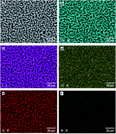 | ||
| Fig. 6 (a) SEM image of the CH3NH3PbI3(Cl) cell containing 5 mg of NH4Cl, and corresponding elemental mapping images of the (b) Pb M line, (c) I L line, (d) Cl K line, (e) C K line, and (f) N K line. | ||
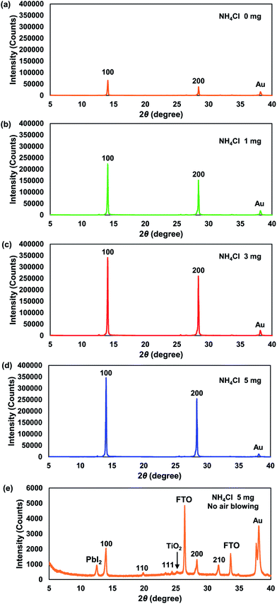
Fig. 7(a)–(d) shows XRD patterns of the FTO/TiO2/CH3NH3PbI3(Cl)/spiro-OMeTAD/Au cells. The diffraction peaks can be indexed by a cubic crystal system (Pm![[3 with combining macron]](https://www.rsc.org/images/entities/char_0033_0304.gif) m) for CH3NH3PbI3(Cl) perovskite thin films. The XRD pattern of a CH3NH3PbI3(Cl) cell prepared without air blowing or PbCl2 is shown in Fig. 7(e). The diffraction peaks of FTO and TiO2 arise from the FTO substrate and TiO2 mesoporous layer, respectively. For ordinary CH3NH3PbI3 cells prepared at 100 °C without air blowing, XRD peaks of PbI2 have been reported41 similarly to those in Fig. 7(e). The intensities of the 100 and 200 peaks of the perovskite phase increase by more than 100 times with air blowing and NH4Cl, as observed in Fig. 7(b)–(d). The 100 and 200 reflections are sufficiently intense that the diffraction peaks of FTO and TiO2 are not readily apparent.
m) for CH3NH3PbI3(Cl) perovskite thin films. The XRD pattern of a CH3NH3PbI3(Cl) cell prepared without air blowing or PbCl2 is shown in Fig. 7(e). The diffraction peaks of FTO and TiO2 arise from the FTO substrate and TiO2 mesoporous layer, respectively. For ordinary CH3NH3PbI3 cells prepared at 100 °C without air blowing, XRD peaks of PbI2 have been reported41 similarly to those in Fig. 7(e). The intensities of the 100 and 200 peaks of the perovskite phase increase by more than 100 times with air blowing and NH4Cl, as observed in Fig. 7(b)–(d). The 100 and 200 reflections are sufficiently intense that the diffraction peaks of FTO and TiO2 are not readily apparent.
The ratios of the 100 diffraction intensities (I100) to the 210 diffraction intensities (I200) of the perovskite crystals were calculated as I100/I210, from the XRD data in Fig. 6. The results are summarized in Table 4. If the CH3NH3PbI3 cubic perovskite particles are randomly oriented, then the I100/I210 value should be 1.81.34 For the cell prepared using air blowing and without NH4Cl, the I100/I210 is 61. This indicates that the (100) planes of the perovskite particles are preferentiality oriented parallel to the FTO substrate. Adding NH4Cl to the cell results in the I100/I210 increasing to 3600, which is 2000 times higher than the I100/I210 of randomly oriented perovskite crystals. The cell prepared with 5 mg of NH4Cl without air blowing or PbCl2 has an I100/I210 of 2.8. This indicates that most of the perovskite particles are randomly oriented. The ratios of the I100 intensities to the FTO substrate intensities (IFTO) were also calculated for the perovskite crystals, and are also shown in Table 4. Using air blowing and NH4Cl increases the I100/IFTO. These results indicate that preferential (100) crystal orientation occurs in films prepared using air blowing with NH4Cl. By using a least squares method, the lattice constants were determined to be 6.274, 6.276, 6.276, 6.276, and 6.275 Å for the cells with NH4Cl 0 mg, 1 mg, 3 mg, 5 mg, and 5 mg without air blow, respectively, and the lattice constants are almost constant for the cell.
Two mechanisms are considered for the formation of the (100)-oriented CH3NH3PbI3(Cl) perovskite crystals. The first mechanism is crystal growth being promoted by air blowing during spin-coating of the perovskite layers. When the CH3NH3PbI3(Cl) solution crystalizes into perovskite particles, fast annealing with air flow accelerates the crystallization of CH3NH3PbI3(Cl). The (100) planes of the perovskite crystals have low surface tension, which results in the growth of (100)-oriented crystals. When highly-oriented crystals are formed, the amount of high angle grain boundaries decreases, which decreases the Rs and increases the VOC. The second mechanism is the formation of a homogeneous morphology during annealing, as a result of the NH4Cl surfactant. Networking structures are formed in cells containing NH4Cl, as observed in Fig. 4(d). This improves the surface coverage and carrier transport, which increases the FF and JSC. The improved conversion efficiency can be described by these two mechanisms.
Cl doping at I sites also promotes the photovoltaic properties of the cells. Excess 2(CH3NH3Cl) could be vaporized from the starting composition of 3(CH3NH3I) + PbCl2.42–44 A small amount of residual Cl is doped into the CH3NH3PbI3 phase, as detected by EDS. The increases the exciton diffusion length,31,33 which increases the JSC. Further investigation is required regarding the specific nanostructures in the cell.
Conclusions
The effects of NH4Cl addition using an air blow method on CH3NH3PbI3(Cl) perovskite solar cells were investigated. The J–V characteristics were improved by introducing an appropriate amount of NH4Cl and air blowing. The resulting cell conversion efficiency was 14%. Microstructure analysis by XRD, OM, SEM, and EDS indicated that highly (100)-orientated perovskite crystals with dense grains were formed when using NH4Cl and air blowing. The I100/I210 ratio of the perovskite crystals was 2000 times higher than that of randomly oriented grains. The (100)-oriented cells were stable during storage for two weeks in ambient air. Formation of the (100)-oriented perovskite crystals was due to the crystal growth accelerated by air blowing during spin-coating. The highly-oriented crystals with decreased grain boundaries could decrease the Rs and increase the VOC. In addition, formation of a homogeneous morphology with networking structures was promoted by the NH4Cl surfactant. Improvement of the surface coverage and carrier transport increased the FF and JSC. As a result, these microstructures improved the conversion efficiency, and this NH4Cl addition combined with an air blow method is an effective method for fabrication of highly crystalline-oriented homogeneous thin films.Conflicts of interest
There are no conflicts to declare.Acknowledgements
This research was supported in part by the Satellite Cluster Program of the Japan Science and Technology Agency. The authors thank A. Suzuki and M. Fukaya of The University of Shiga Prefecture, Japan, for their invaluable support. They also thank Aidan G. Young, PhD, from Edanz Group (www.edanzediting.com/ac) for editing a draft of this manuscript.References
- A. Kojima, K. Teshima, Y. Shirai and T. Miyasaka, J. Am. Chem. Soc., 2009, 131, 6050–6051 CrossRef CAS PubMed.
- J.-H. Im, C.-R. Lee, J.-W. Lee, S.-W. Park and N.-G. Park, Nanoscale, 2011, 3, 4088–4093 RSC.
- H. S. Kim, C. R. Lee, J. H. Im, K. B. Lee, T. Moehl, A. Marchioro, S. J. Moon, R. Humphry-Baker, J. H. Yum, J. E. Moser, M. Grätzel and N. G. Park, Sci. Rep., 2012, 2, 591–597 CrossRef PubMed.
- M. M. Lee, J. Teuscher, T. Miyasaka, T. N. Murakami and H. J. Snaith, Science, 2012, 338, 643–647 CrossRef CAS PubMed.
- J. Burschka, N. Pellet, S. J. Moon, R. Humphry-Baker, P. Gao, M. K. Nazeeruddin and M. Grätzel, Nature, 2013, 499, 316–320 CrossRef CAS PubMed.
- H. Zhou, Q. Chen, G. Li, S. Luo, T.-B. Song, H.-S. Duan, Z. Hong, J. You, Y. Liu and Y. Yang, Science, 2014, 345, 542–546 CrossRef CAS PubMed.
- G. Fu, L. Hou, Y. Wang, X. Liu, J. Wang, H. Li, Y. Cui, D. Liu, X. Li and S. Yang, Sol. Energy Mater. Sol. Cells, 2017, 165, 36–44 CrossRef CAS.
- J. Zheng, M. Zhang, C. F. J. Lau, X. Deng, J. Kim, Q. Ma, C. Chen, M. A. Green, S. Huang and A. W. Y. Ho-Baillie, Sol. Energy Mater. Sol. Cells, 2017, 168, 165–171 CrossRef CAS.
- W. S. Yang, J. H. Noh, N. J. Jeon, Y. C. Kim, S. Ryu, J. Seo and S. I. Seok, Science, 2015, 348, 1234–1237 CrossRef CAS PubMed.
- M. Saliba, T. Matsui, J. Y. Seo, K. Domanski, J. P. Correa-Baena, M. K. Nazeeruddin, S. M. Zakeeruddin, W. Tress, A. Abate, A. Hagfeldtd and M. Grätzel, Energy Environ. Sci., 2016, 9, 1989–1997 CAS.
- M. Saliba, S. Orlandi, T. Matsui, S. Aghazada, M. Cavazzini, J. P. Correa-Baena, P. Gao, R. Scopelliti, E. Mosconi, K. H. Dahmen, F. De Angelis, A. Abate, A. Hagfeldt, G. Pozzi, M. Graetzel and M. K. Nazeeruddin, Nat. Energy, 2016, 1, 15017 CrossRef CAS.
- D. Bi, W. Tress, M. I. Dar, P. Gao, J. Luo, C. Renevier, K. Schenk, A. Abate, F. Giordano, J. P. C. Baena, J. D. Decoppet, S. M. Zakeeruddin, M. K. Nazeeruddin, M. Grätzel and A. Hagfeldt, Sci. Adv., 2016, 2, 1501170 Search PubMed.
- D. Bi, C. Yi, J. Luo, J.-D. Décoppet, F. Zhang, S. M. Zakeeruddin, X. Li, A. Hagfeldt and M. Grätzel, Nat. Energy, 2016, 1, 16142 CrossRef CAS.
- M. Saliba, T. Matsui, K. Domanski, J.-Y. Seo, A. Ummadisingu, S. M. Zakeeruddin, J.-P. Correa-Baena, W. R. Tress, A. Abate, A. Hagfeldt and M. Grätzel, Science, 2016, 354, 206–209 CrossRef CAS PubMed.
- M. He, B. Li, X. Cui, B. Jiang, Y. He, Y. Chen, D. O'Neil, P. Szymanski, M. A. EI-Sayed, J. Huang and Z. Lin, Nat. Commun., 2017, 8, 16045 CrossRef CAS PubMed.
- S. S. Shin, E. J. Yeom, W. S. Yang, S. Hur, M. G. Kim, J. Im, J. Seo, J. H. Noh and S. I. Seok, Science, 2017, 356, 167–171 CrossRef CAS PubMed.
- Z. Tang, T. Bessho, F. Awai, T. Kinoshita, M. M. Maitani, R. Jono, T. N. Murakami, H. Wang, T. Kubo, S. Uchida and H. Segawa, Sci. Rep., 2017, 7, 12183 CrossRef PubMed.
- J.-M. Wang, Z.-K. Wang, M. Li, C.-C. Zhang, L.-L. Jiang, K.-H. Hu, Q.-Q. Ye and L.-S. Liao, Adv. Energy Mater., 2017, 7, 1701688 Search PubMed.
- F. Hao, C. C. Stoumpos, D. H. Cao, R. P. H. Chang and M. G. Kanatzidis, Nat. Photonics, 2014, 8, 489–494 CrossRef CAS.
- W. Liao, D. Zhao, Y. Yu, N. Shrestha, K. Ghimire, C. R. Grice, C. Wang, Y. Xiao, A. J. Cimaroli, R. J. Ellingson, N. J. Podraza, K. Zhu, R.-G. Xiong and Y. Yan, J. Am. Chem. Soc., 2016, 138, 12360–12363 CrossRef CAS PubMed.
- T. Oku, Y. Ohishi and A. Suzuki, Chem. Lett., 2016, 45, 134–136 CrossRef CAS.
- T. Oku, Y. Ohishi, A. Suzuki and Y. Miyazawa, Metals, 2016, 6, 147 CrossRef.
- J. Zhang, M. H. Shang, P. Wang, X. Huang, J. Xu, Z. Hu, Y. Zhu and L. Han, ACS Energy Lett., 2016, 1, 535–541 CrossRef CAS.
- T. Oku, Y. Ohishi and A. Suzuki, AIP Conf. Proc., 2017, 1807, 020007 CrossRef.
- Y. Ando, T. Oku and Y. Ohishi, Jpn. J. Appl. Phys., 2018, 57, 02CE02 CrossRef.
- Y. Shirahata and T. Oku, Phys. Status Solidi A, 2017, 214, 1700268 CrossRef.
- A. Hamatani, Y. Shirahata, Y. Ohishi, M. Fukaya and T. Oku, Adv. Mater. Phys. Chem., 2017, 7, 1–10 CrossRef.
- T. Krishnamoorthy, H. Ding, C. Yan, W. L. Leong, T. Baikie, Z. Zhang, M. Sherburne, S. Li, M. Asta, N. Mathews and S. G. Mhaisalkar, J. Mater. Chem. A, 2015, 3, 23829–23832 CAS.
- Y. Ohishi, T. Oku and A. Suzuki, AIP Conf. Proc., 2016, 1709, 020020 CrossRef.
- W. Peng, X. Miao, V. Adinolfi, E. Alarousu, O. El Tall, A. H. Emwas, C. Zhao, G. Walters, J. Liu, O. Ouellette, J. Pan, B. Murali, E. H. Sargent, O. F. Mohammed and O. M. Bakr, Angew. Chem., Int. Ed., 2016, 55, 10686–10690 CrossRef CAS PubMed.
- S. D. Stranks, G. E. Eperon, G. Grancini, C. Menelaou, M. J. P. Alcocer, T. Leijtens, L. M. Herz, A. Petrozza and H. J. Snaith, Science, 2013, 342, 341–344 CrossRef CAS PubMed.
- T. Oku, K. Suzuki and A. Suzuki, J. Ceram. Soc. Jpn., 2016, 124, 234–238 CrossRef CAS.
- Q. Dong, Y. Fang, Y. Shao, P. Mulligan, J. Qiu, L. Cao and J. Huang, Science, 2015, 347, 967–970 CrossRef CAS PubMed.
- T. Oku, Solar Cells and Energy Materials, Walter de Gruyter, Berlin, 2017 Search PubMed.
- W. Nie, H. Tsai, R. Asadpour, J. C. Blancon, A. J. Neukirch, G. Gupta, J. J. Crochet, M. Chhowalla, S. Tretiak, M. A. Alam, H. L. Wang and A. D. Mohite, Science, 2015, 347, 522–525 CrossRef CAS PubMed.
- J.-W. Lee, S.-H. Bae, N. D. Marco, Y. T. Hsieh, Z. Dai and Y. Yang, Materials Today Energy, 2018, 7, 149–160 CrossRef.
- C. Zuo and L. Ding, Nanoscale, 2014, 6, 9935–9938 RSC.
- J. He and T. Chen, J. Mater. Chem. A, 2015, 3, 18514–18520 CAS.
- T. Oku, Y. Ohishi, A. Suzuki and Y. Miyazawa, J. Ceram. Soc. Jpn., 2017, 125, 303–307 CrossRef CAS.
- T. Oku and Y. Ohishi, J. Ceram. Soc. Jpn., 2018, 126, 56 CrossRef CAS.
- T. Oku, M. Zushi, Y. Imanishi, A. Suzuki and K. Suzuki, Appl. Phys. Express, 2014, 7, 121601 CrossRef.
- H. Yu, F. Wang, F. Xie, W. Li, J. Chen and N. Zhao, Adv. Funct. Mater., 2014, 24, 7102–7108 CAS.
- A. Dualeh, N. Tétreault, T. Moehl, P. Gao, M. K. Nazeeruddin and M. Grätzel, Adv. Funct. Mater., 2014, 24, 3250–3258 CrossRef CAS.
- J. A. McLeod, Z. Wu, B. Sun and L. Liu, Nanoscale, 2016, 8, 6361–6368 RSC.
- H. J. Snaith, A. Abate, J. M. Ball, G. E. Eperon, T. Leijtens, N. K. Noel, S. D. Stranks, J. T.-W. Wang, K. Wojciechowski and W. Zhang, J. Phys. Chem. Lett., 2014, 5, 1511–1515 CrossRef CAS PubMed.
- Z. Tang, S. Uchida, T. Bessho, T. Kinoshita, H. Wang, F. Awai, R. Jono, M. M. Maitani, J. Nakazaki, T. Kubo and H. Segawa, Nano Energy, 2018, 45, 184–192 CrossRef CAS.
Footnote |
| † Electronic supplementary information (ESI) available. See DOI: 10.1039/c7ra13582c |
| This journal is © The Royal Society of Chemistry 2018 |

