
Manipulating the crystallization and interfacial charge behavior with a jellyfish-like molecular template for efficient perovskite solar cells†
Haoyan
Wang
a,
Chenyu
Zhao
a,
Lin
Fan
 ab,
Maobin
Wei
ab,
Huilian
Liu
ab,
Xiaoyan
Liu
ab,
Jinghai
Yang
*ab,
Fengyou
Wang
*ab and
Lili
Yang
*ab
ab,
Maobin
Wei
ab,
Huilian
Liu
ab,
Xiaoyan
Liu
ab,
Jinghai
Yang
*ab,
Fengyou
Wang
*ab and
Lili
Yang
*ab
aKey Laboratory of Functional Materials Physics and Chemistry of the Ministry of Education, Jilin Normal University, Changchun 130103, China. E-mail: jhyang1@jlnu.edu.cn; wfy@jlnu.edu.cn; llyang1980@163.com
bNational Demonstration Center for Experimental Physics Education, Jilin Normal University, Siping 136000, China
First published on 11th December 2023
Abstract
The buried electron-transport layer (ETL)/perovskite interface is crucial for the performance of n-i-p-type perovskite solar cells. However, the presence of nonuniform distributed dangling bonds on the mainstream metal oxide ETL surface leads to nonradiative recombination and affects the homogenization of the perovskite film by triggering disordered nucleation. To address these challenges, we modulated the ETL/perovskite interface by introducing a jellyfish-like molecular template (JLMT), where the jellyfish foot was glycine and the jellyfish head was MoS2, to simultaneously achieve highly oriented perovskite films and efficient interfacial charge transfer. Glycine was first anchored on the ETL through esterification. Then, sequentially layered MoS2 was deposited on the surface. The lower reduction potential of glycine with respect to that of MoS2 drives electron transfer from glycine to MoS2, leading to surface charge doping and building a favorable bandgap alignment at the ETL/perovskite interface. In addition, the top surface of MoS2, which is free from dangling bonds, could guide the orientational growth of the perovskite because of its lattice structural compatibility. An as-fabricated JLMT device achieved a champion power conversion efficiency (PCE) of 21.76% and an open-circuit voltage (Voc) of 1.20 V. Furthermore, under room temperature conditions with a relative humidity of ∼30%, the PCE of the JLMT device retained 93% of its initial value after 30 days, whereas the control device only retained around 61% of its initial PCE.
1. Introduction
In just a dozen years, the power conversion efficiency (PCE) of perovskite solar cells (PSCs) has skyrocketed rapidly from 3.8% to 26.1% (certified in 2023) owing to their high optical absorption coefficient and long carrier diffusion length (>1 μm).1,2 In regular-structure (n-i-p) planar perovskite solar cells (PSCs), the perovskite absorption layer, primarily prepared through a solution process, is sandwiched between the electron-transport layer (ETL) and the hole-transport layer (HTL). The ETL/perovskite interface is crucial because it not only affects the nucleation and growth process of the perovskite but also dominates photogenerated electron extraction and transfer.3 Various metal oxides (TiO2, SnO2, ZnO, etc.) are selected as ETLs due to their excellent electron mobility, high light transmittance, and good band alignment with perovskite.4 However, during the preparation process, the formation of metal oxide ETLs leads to inevitable valence bond breaking (specifically, metal–oxygen bonds), resulting in a nonuniform distribution of dangling bonds on the surface. These dangling bonds can adversely affect the homogenization of the perovskite film by inducing disordered nucleation.5 In addition, recent studies have found that dangling bonds existing on the surfaces of metal oxides can interact with moisture to form hydroxyl (–OH) groups, which act as Brønsted bases and undergo a deprotonation reaction with the perovskite, leading to a deterioration in its framework and stability.6 Meanwhile, dangling bond defects can also induce interfacial carrier nonradiative recombination, hindering further enhancement of the PCE and stability of PSCs.7 Therefore, terminating dangling bonds on the surface of metal oxides is a key factor in improving perovskite crystallization and stability and accelerating carrier transport to achieve high-performance PSCs.Several carboxyl-containing molecules, such as amino acids, carboxylic acids, and diethanolamine, have been self-assembled on ETLs (metal oxides) by esterification to minimize interfacial dangling bonds.8–10 However, the film homogeneity can be influenced by the nonuniform distribution of extra groups or chemical bonds in the modifiers. In addition to organic groups, many inorganic materials such as carbon-based materials11–15 and metallic compounds are employed to modify the perovskite interface. In an earlier study, we introduced an inorganic amorphous metal nitride (a-TiNx) layer at the ETL/perovskite interface to eliminate the dangling bonds through coordination interactions with nitride atoms.16 However, due to the uncertain valence states of the metal ions in the amorphous state, uncoordinated metal ions still exist on the surface of the a-TiNx interlayer, resulting in the formation of dangling bonds.
In addition to the aforementioned approaches, van der Waals (vdW) epitaxy is also a common technique for preparing high-quality semiconductor films with preferential orientations on smooth and dangling-bond-free surfaces.17–20 Inspired by these intriguing effects, 2D materials with proper lattice parameters have been utilized as growth templates for preparing high-quality perovskite films with a controllable orientation and less defect interface, thereby improving photovoltaic performance and stability. As a typical representative, molybdenum disulfide (MoS2) is a promising 2D transition metal dichalcogenide (TMD) with a dangling-bond-free surface and a matched lattice with perovskite. The interplane distances of MAPbI3 (008) and MoS2 (110) planes have an identical value of 1.58 Å, which lays a foundation for perovskite epitaxy growth.21,25
However, it is worth noting that the energy level of MoS2 (∼3.4–5.2 eV) is mismatched with the perovskite in n-i-p PCSs, and an unfavorable bandgap offset will thus be established at the MoS2/perovskite interface, hindering the interfacial carrier transfer.23 Fortunately, previous studies have demonstrated that surface charge doping by strong electron-donating groups can alter the Fermi level and subsequently adjust the energy level structure of MoS2, which is promising for achieving energy level alignment between MoS2 and perovskite.24–27
Accordingly, in this work, a jellyfish-like molecular template (JLMT), where the jellyfish foot was glycine and the jellyfish head was MoS2, was developed to modulate the ETL/perovskite interface for simultaneously achieving highly oriented perovskite films and boosting the interfacial charge transfer. Glycine was first anchored on the SnO2 ETL through esterification; then, MoS2 was absorbed on the glycine by solution spin coating. The lower reduction potential of glycine with respect to that of MoS2 drives electron transfer from glycine to MoS2, forming surface charge doping and building a favorable bandgap alignment at the ETL/perovskite interface. Notably, the surface charge doping did not induce any dangling bonds in MoS2 lattice, which maintained the oriented epitaxial growth of perovskite on the MoS2 surface. An as-fabricated JLMT PSC exhibited a significantly improved photovoltaic performance and reduced hysteresis behavior, yielding a champion PCE of 21.76% accompanied by an open-circuit voltage (Voc) of 1.20 V, which is one of the highest PCEs for MAPbI3 solar cells. Meanwhile, the PCE retained 93% of its value under room temperature conditions with a relative humidity (RH) of 30% compared with the control devices after 30 days.
2. Results and discussion
To confirm the phase of the MoS2 nanosheet, we conducted X-ray diffraction (XRD) and Raman spectroscopy analyses of the samples. The XRD pattern of the target MoS2 nanosheet was matched with the standard diffraction pattern of the 2H-phase layered MoS2 file (JCPDS#37-1492). Three diffraction peaks centered at 14.5°, 32.9°, and 58.5° could be observed, corresponding to the (002), (100), and (110) planes of MoS2 nanosheet.28 The Raman spectrum showed the presence of two peaks at ∼378 cm−1 and ∼402 cm−1, which corresponded to the in-plane E2g and out-of-plane A1g vibration modes of the 2H-phase MoS2.22,29 Subsequently, we explored the structure information using transmission electron microscopy (TEM) and high-resolution transmission electron microscopy (HRTEM). As shown in Fig. 1c, the TEM image revealed the layered structure of MoS2. Energy-dispersive X-ray spectroscopy (EDS) analysis confirmed the uniform distribution of both Mo and S elements within the layered MoS2 structure (Fig. S1†). Further analysis using HRTEM allowed the clear identification of lattice fringes with a spacing of 0.316 nm, corresponding to the (004) plane of 2H MoS2 (inset in Fig. 1c).29,30 To determine the thickness of the MoS2 nanosheet, atomic force microscopy (AFM) was employed. The AFM image, as shown in Fig. S2,† indicated an average thickness of ∼1.5 nm.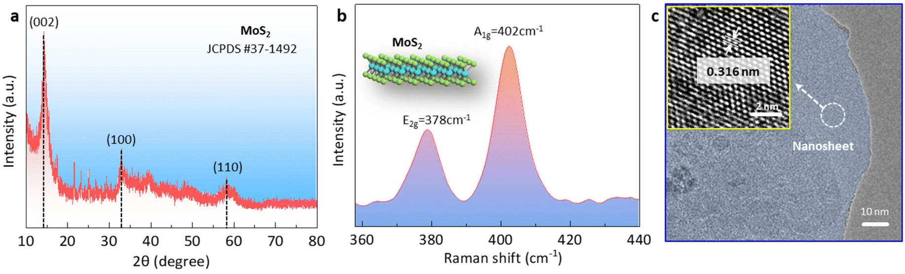 | ||
| Fig. 1 Properties of the MoS2 nanosheets. (a) XRD pattern, (b) Raman spectra, and (c) TEM and HRTEM images. | ||
The growth of MAPbI3 on MoS2 surface was further monitored. MoS2 nanosheets were drop-coated on a carbon-coated copper grid; then a precursor solution of MAPbI3 was spin-coated on the sample surfaces and solidified by an anti-solvent method, followed by thermal annealing at 100 °C for 10 min, which was similar to the perovskite film preparation procedure in PSCs. Next, the samples were characterized using HRTEM. Fig. 2a shows the typical TEM image of the as-synthesized heterostructure in which the MAPbI3 film can be seen to be partially covering the surface of a MoS2 nanosheet. Fig. 2b and c show the HRTEM images of the MoS2 and MAPbI3 regions, respectively. The presence of clear lattice fringes indicated the high quality of both the MoS2 nanosheet and the MAPbI3 grain. The lattice fringe with a distance of 1.58 Å corresponded to the (110) plane of MoS2, while the lattice fringe with a distance of 3.16 Å corresponded to the (004) plane of the MAPbI3 grain. Fig. 2d and e display the selected area electron diffraction (SAED) patterns of pure MoS2 and MAPbI3, respectively, which serve as reference patterns. The SAED pattern of the overlapping area between MAPbI3 and MoS2 revealed the relative crystallographic orientation of the MAPbI3 layer and MoS2 crystal in the heterostructure (Fig. 2f). The SAED pattern exhibited two sets of diffraction spots with square (red) and hexagonal (yellow) symmetries. Each diffraction spot in the smaller and larger hexagonal patterns corresponded to the (100) and (110) family planes of the MoS2 crystal, respectively. Each diffraction spot in the square pattern could be indexed to the (004) family plane of the MAPbI3 layer. Intriguingly, based on the literature,19,21 it is worth noting that the interplane distances of the (008) plane of MAPbI3 and the (110) plane of MoS2 are identical, measuring 1.58 Å. Consequently, this suggests that the in-plane coupling between MoS2 and MAPbI3 may facilitate the preferential growth of MAPbI3 grains along the (110) plane on the surface of the MoS2 templates. This concept is schematically illustrated in Fig. S3.† In Fig. 2f, it can be observed that the (008) plane of MAPbI3 perfectly overlapped with the (110) plane of MoS2, providing evidence for the impeccable lattice match between these two planes. Thus, it confirms that the MAPbI3 layer exhibited epitaxial growth on the MoS2 nanosheet.
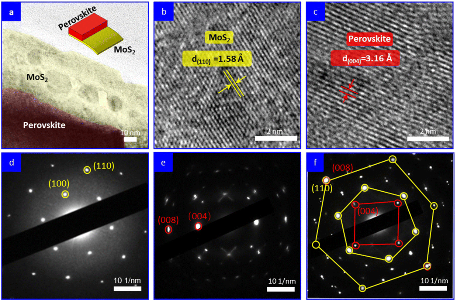 | ||
| Fig. 2 MAPbI3 epitaxially grown on MoS2. (a) Top-view TEM image of MoS2 with a MAPbI3 layer grown on its surface. (b and c) HRTEM images of MoS2 and MAPbI3, respectively. (d and e) SAED patterns of MoS2 and MAPbI3 as reference patterns, respectively. (f) SAED pattern of MAPbI3/MoS2 region, where two distinct diffraction spots can be observed, with the yellow spots representing MoS2 and the red spots representing MAPbI3. | ||
Scanning electron microscopy (SEM) and X-ray diffraction (XRD) were used to investigate the crystallization of MAPbI3 grown on MoS2. The SEM analysis revealed that the MAPbI3 film grown on the MoS2 substrate (MoS2-MAPbI3) exhibited larger grains and fewer boundaries compared with the control film grown on the SnO2 substrate. The grain size of MAPbI3 increased by ∼300 nm when grown on MoS2, indicating the improved crystallization (Fig. 3a and Fig. S4†). Next, X-ray diffraction (XRD) measurements were performed to study the crystal orientation of MAPbI3. The (110) peak intensity of the MoS2-MAPbI3 film was markedly stronger than that of the control film (7085.53 a.u. versus 5176.65 a.u.). The increased relative intensity of (110)/(310) (from 5.42 to 6.93 a.u.) suggested the preferential orientation along the (110) direction21,30 (Fig. 3b). Further analysis was conducted using grazing incidence wide-angle X-ray scattering (GIWAXS) on the corresponding films to examine the effect of MoS2 on the crystal orientation of MAPbI3. Fig. 3c shows the 2D GIWAXS patterns of the MAPbI3 and MoS2-MAPbI3 films. Compared to the MAPbI3 film, the MoS2-MAPbI3 film exhibited a more distinct diffraction ring at q = 1 Å−1, which corresponded to the (110) plane. The intensity distribution range around the azimuthal angle of 90° was narrower for the MoS2-MAPbI3 films, indicating an improved orientation of the MoS2-MAPbI3 films (Fig. 3d).21 These observed phenomena could be attributed to two factors: (1) the matching lattice structure between the (008) plane of MAPbI3 and the (110) plane of MoS2, which promoted the growth of MAPbI3 along the (110) plane; and (2) the dangling-bond-free surface of MoS2, which facilitated the migration of radicals and increased the grain boundary mobility. This accelerated the lateral growth of perovskite grains and led to an enlargement of the perovskite grain size.20,30
 | ||
| Fig. 3 Crystallization of MoS2-MAPbI3. (a) SEM images of the MAPbI3 and MoS2-MAPbI3 films. (b) XRD patterns of the MAPbI3 film and MoS2-MAPbI3 film. (c) 2D GIWAXS patterns for the MAPbI3 and MoS2-MAPbI3 films. (d) Azimuthal pole plot of (110) diffraction for the MoS2-MAPbI3 and MAPbI3 films prepared under the same conditions. | ||
Furthermore, planar perovskite solar cells with an architecture of Glass/ITO/SnO2/with- and without MoS2/MAPbI3/Spiro-OMeTAD/Ag were fabricated (Fig. 4a). Typically, an improved perovskite crystallinity leads to increased device efficiency due to the presence of fewer defects and reduced nonradiative recombination. However, the statistical analysis of 20 devices (10 MAPbI3-devices and 10 MoS2-MAPbI3-devices) showed that the PCE, as well as the other key parameters of the devices (i.e., Voc, Jsc, FF), decreased from 18.59 ± 0.3% to 17.24 ± 0.4% following MoS2 application (Fig. 4b–e). Since the preparation process of the devices with and without MoS2 was the same, we suspected that the decreased PCE may be related to the interface properties. Previous work has shown that the energy level of MoS2 (∼3.4–5.2 eV) is mismatched with that of MAPbI3 (∼3.9–5.4 eV),31,32 resulting in an interfacial energy barrier that blocks charge transport and further reduces device efficiency. To validate this assumption, we measured the ultraviolet photoelectron spectra (UPS) and UV-vis absorption spectra of MoS2 and MAPbI3, respectively. The conduction band (EC), Fermi energy (EF), and valence band (EV) of MoS2 were −3.46, −4.58, and −5.20 eV, while those of MAPbI3 were −3.93, −4.50, and −5.43 eV, respectively (Fig. S5 and S6†). Therefore, the energy level structure between MoS2 and MAPbI3 can be depicted as shown in Fig. 4f. Under thermal equilibrium, a band offset is formed, which hinders electron extraction and decreases the device PCE.
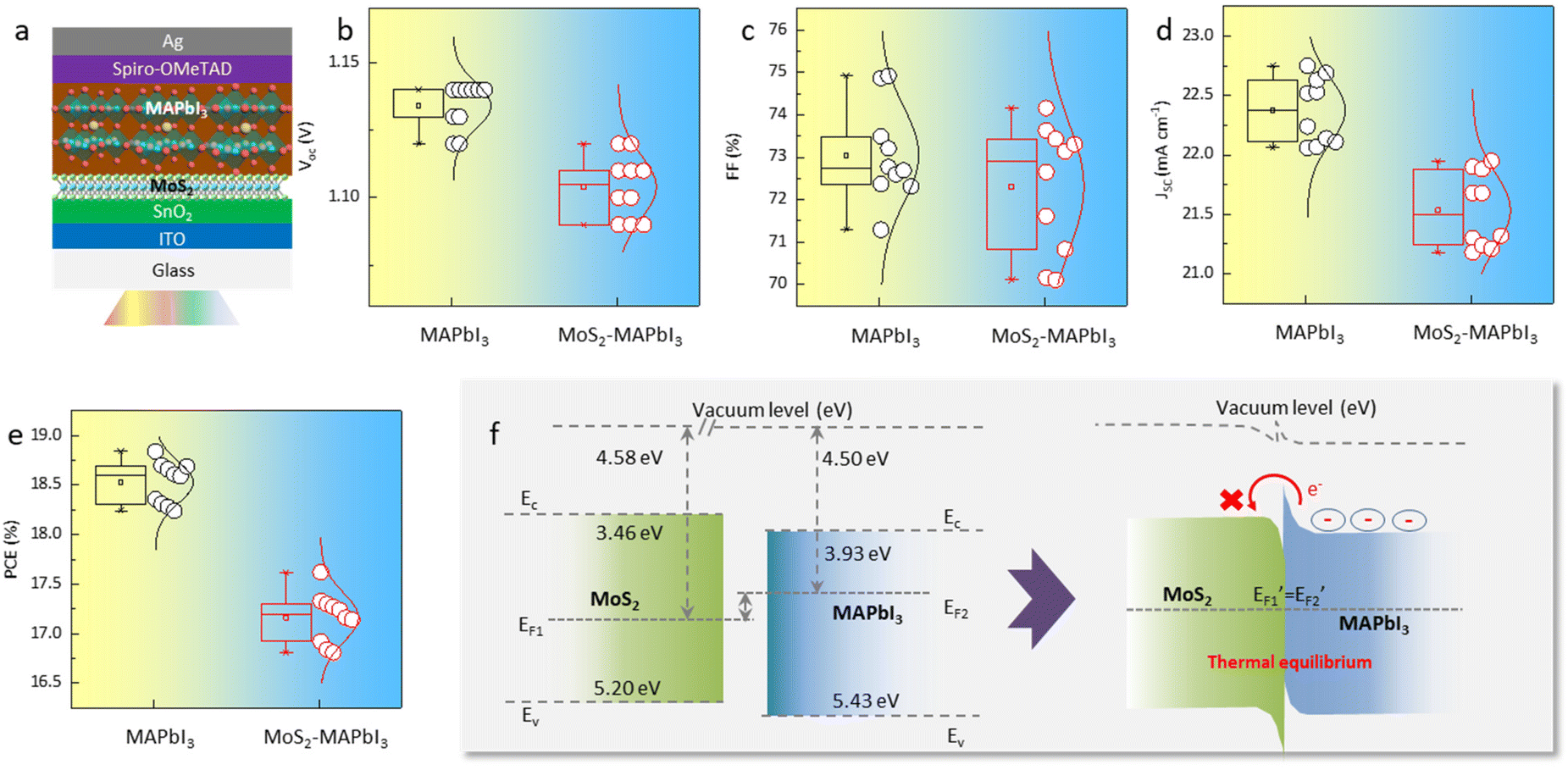 | ||
| Fig. 4 Bandgap alignment between MoS2 and MAPbI3. (a) Schematic structure of the MoS2-MAPbI3 device. (b–e) Distribution of VOC, JSC, FF, and PCE values collected from 10 MAPbI3 and 10 MoS2-MAPbI3 devices. (f) Energy level change scheme of MoS2 and MAPbI3. | ||
Accordingly, it is crucial to realign the energy level structure of MoS2 to enhance electron extraction at the MoS2-MAPbI3 interface and further improve device performance. Chemical doping is a common approach for regulating the energy levels and electronic properties of different types of transition metal dichalcogenides (TMDCs), including MoS2 and WSe2. In particular, surface-charge-transfer doping, achieved by adsorbing specific electron-donating or electron-withdrawing groups on the surfaces of TMDCs, has been demonstrated as an effective method in previous studies. For instance, Javey et al.25 utilized benzyl viologen (BV) as a surface-charge-transfer donor for MoS2 flakes to regulate their energy levels. The high reduction potentials of BV promoted electron transfer from BV molecules to MoS2 flakes, resulting in n-type doping and an elevation of the Fermi level in the MoS2 flakes. Similarly, Du et al. achieved n-type doping in MoS2 by immersing it in an amine-rich aliphatic polymer (PEI) solution.33 This realignment of energy levels led to reduced sheet resistance and contact resistance in multilayer MoS2 field-effect transistors.
In this work, it was important to note that this doping method may introduce additional functional groups on the both sides of the MoS2 layer, which could disrupt the templating function of MoS2 and affect the epitaxial growth of MAPbI3.25,34 To overcome this challenge, we employed glycine as the dopant and proposed a single-side bonding method to construct a jellyfish-like molecular template (JLMT), where glycine served as the jellyfish foot, and MoS2 as the jellyfish head (Fig. 5a). The preparation process is illustrated in Fig. 5b. Initially, glycine was anchored on the SnO2 substrate through esterification between the –COOH group of glycine and the –OH group on the SnO2 surface. Subsequently, MoS2 was coated on the substrate and absorbed onto the glycine surface. Fig. S7† shows the lowest occupied molecular orbital (LUMO), Fermi level (EF), and the highest occupied molecular orbital (HOMO) of glycine, which were −0.50 eV, −3.48 eV, and −7.24 eV, respectively. Additionally, the HOMO and LUMO energies of glycine were determined using density functional theory calculations, as shown in Fig. 5c; these values were consistent with the measured results (HOMO: −7.19 eV and LUMO: −0.48 eV). The energy diagram illustrated in Fig. 5c displays the energy levels of both MoS2 and glycine. Owing to its higher ionization potential and LUMO level, glycine acts as an electron donor to MoS2, leading to alterations in its internal electron arrangement as well as changes in its energy level structure (as depicted in Fig. 5c).35 To validate the above proposition, Kelvin probe force microscopy (KPFM) was used to characterize the surface potentials of MoS2 and MoS2-glycine (Fig. 5d). The contact potential difference (CPD) of MoS2 was measured as 269.56 mV, whereas that of MoS2-glycine increased to 387.34 mV, indicating an upward shift in the EF of MoS2.36
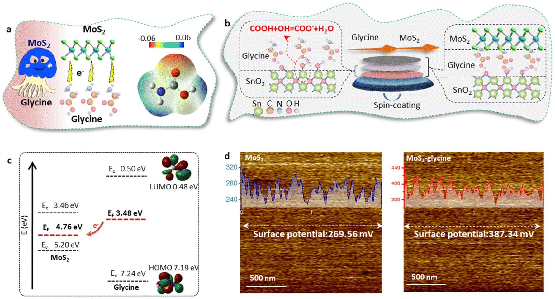 | ||
| Fig. 5 Formation mechanism of JLMT (a) Jellyfish-like structure consisting of MoS2 and glycine. (b) Preparation method used to construct the JLMT (c) Electron-transfer scheme between MoS2 and glycine. (d) KPFM mapping of MoS2 and MoS2-glycine. Inset: CPD profile along the horizontal marked lines. | ||
Moreover, the formation mechanism of JLMT was also investigated in detail. We first used X-ray photoelectron spectroscopy (XPS) to study the esterification between SnO2 and glycine. The Sn 3d XPS peaks of glycine-SnO2 shifted to higher binding energies compared with the pure SnO2 film (Fig. 6a). In addition, the O 1s spectrum of the pristine SnO2 film plotted in Fig. 6b showed a broad asymmetric peak, which could be deconvoluted into lattice oxygen (530.34 eV) and chemisorbed oxygen atoms or hydroxyl groups (531.25 eV). The peak intensity of the lattice oxygen decreased while that of the adsorbed oxygen increased (Fig. 6c), demonstrating the change in the chemical circumstance of oxygen atoms in the lattice of SnO2 surface after the treatment. These results support the view that glycine was successfully anchored on to SnO2 by esterification. Fourier-transform infrared spectroscopy (FTIR) was performed and the high-resolution Mo 3d and S 2p core level XPS spectra were recorded to explore the interaction between MoS2 and glycine. After depositing MoS2 on glycine, the N–H vibrations of glycine were red-shifted from 1634 and 3436 cm−1 to 1629 and 3430 cm−1 (Fig. 6d). The XPS spectra showed that the characteristic peaks of the Mo4+ 3d3/2 and Mo4+ 3d5/2 doublets of pure MoS2 located at 232.5 and 229.0 eV were shifted to a higher binding energy after depositing on glycine (Fig. 6e). Similarly, the S 2p3/2 and 2p1/2 peaks were also shifted to higher binding energies (Fig. 6f). These results imply that the EF of MoS2 experienced an upward shift to the EC due to the surface-charge-transfer doping.37,38 Raman spectroscopy was also performed to explore the electronic information of MoS2 (Fig. 6g). The peak at ∼378 cm−1 corresponded to the E12g mode and was due to the displacement of Mo and S atoms within the basal plane, whereas the A1g mode at ∼402 cm−1 originated from the vibration perpendicular to the basal plane.39 Several studies have suggested that the E12g mode is almost inert, but the A1g mode of MoS2 will undergo a red-shift after n-type doping. In this case, a small red-shift of ∼0.3 cm−1 was observed for the A1g mode when MoS2 was layered on the glycine, indicating successful n-type doping.40 UPS was measured to further quantify the energy level of the glycine-doped MoS2 (Fig. S8†). After treatment with glycine, the EF of MoS2 increased from −4.58 to −4.05 eV, indicating n-type doping and supporting the aforementioned conclusion. The energy level structure diagram of MoS2-glycine and MAPbI3 is depicted in Fig. 6h. Under thermal equilibrium, the alignment of the energy levels between MoS2-glycine and MAPbI3 creates a charge-transfer channel. This interface energy level structure is more conducive to electron extraction and hole blocking, alleviating the previously mentioned problem of interface energy level mismatch and thus improving the efficiency of interface charge transfer. The PL intensity of the JLMT-MAPbI3 device was weaker than that of the control device, while the TRPL lifetime with JLMT-MAPbI3 was shorter. Details on the lifetime parameters are summarized in Table S1.† These findings verified that the introduction of the JLMT accelerated carrier extraction, which could be attributed to a reduction in the interfacial energy barrier at the ETL/perovskite interface.36
 | ||
| Fig. 6 Interactions between glycine, SnO2, and MoS2. (a) XPS spectra of the Sn 3d signals of SnO2 and SnO2-glycine. (b and c) XPS spectra of the O 1s of SnO2 and SnO2-glycine. (d) FTIR spectra of glycine and MoS2-glycine. (e and f) XPS spectra of the Mo 3d and S 3d signals for MoS2 and MoS2-glycine, respectively. (g) Raman shifts of MoS2 and MoS2-glycine. (h) Schematic diagram of the bandgap alignment at the MoS2-glycine/MAPbI3 interface. | ||
Planar PSCs were fabricated with an ITO/SnO2/JLMT/MAPbI3/Spiro-OMeTAD/Ag structure (Fig. 7a). The cross-sectional SEM of the JLMT device showed large grains throughout the perovskite layer compared with the control device (Fig. 7b). The control device showed a PCE of 18.48% with a hysteresis index (HI = (PCEreverse − PCEforward)/PCEreverse) of 7.41%. The champion PCE of the JLMT device increased to 21.76% with an HI value of 1.19% (Fig. 7c). The Voc, Jsc, and FF values were also improved and are summarized in Table S2.† The mean and standard deviation (SD) values of the key parameters of the PSCs are shown in Table S3.† As mentioned above, the introduction of the JLMT created a more favorable bandgap alignment and minimized the energy barriers, leading to enhanced charge extraction and reduced charge recombination at the ETL/perovskite interface. These improvements significantly contributed to the enhancement of the Jsc and FF values. Moreover, in terms of the Voc, the use of the JLMT contributed to improved perovskite crystallization and a reduction in interface defects between the SnO2 and perovskite layers. This effect minimized the charge trapping sites both in the bulk of the perovskite and at the ETL/perovskite interface. As a result, the JLMT promoted more efficient charge separation and reduced the nonradiative recombination, ultimately leading to an enhanced Voc. The integrated Jsc values obtained from the external quantum efficiency (EQE) spectra (Fig. 7d) were 19.94 and 21.41 mA cm−2 for the control and JLMT devices, respectively, which were consistent with the tendency of the J–V results. The operational stabilities of the control and JLMT devices were examined under the maximum power point voltage (Vmpp), respectively. The stabilized PCE of the champion JLMT device reached 20.92% at a Vmpp of 1.00 V, along with a photocurrent density (Jph) of 20.92 mA cm−2, whereas that of the control device was 17.94% at a maximum power point voltage of 0.92 V, along with a Jph of 19.51 mA cm−2 (Fig. 7e).
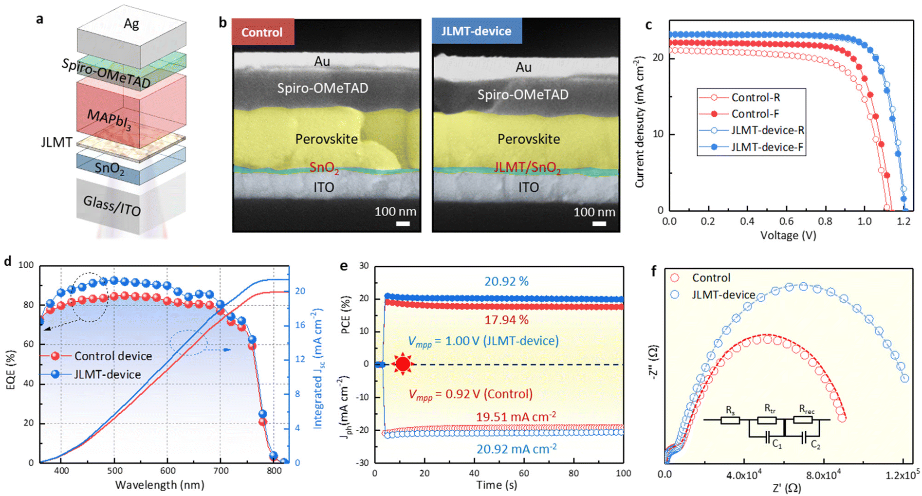 | ||
| Fig. 7 Device performance (a) Whole device structure. (b) Cross-sectional SEM images of the control and JLMT devices. (c) Illuminated J–V curves of the control and JLMT devices. (d) EQE spectra and integrated photocurrent of the control and JLMT devices. (e) PCE and output current density measured at the Vmpp of the control and JLMT devices. (f) Nyquist plots of the control and JLMT devices. The inset shows the equivalent circuit model. | ||
The main reason for the improved photovoltaic performance of the device was the improvement of the crystal quality of the perovskite by the JLMT, which reduced the recombination losses within the device. Simultaneously, the cascaded energy level structure between the JLMT and perovskite also facilitated the efficient extraction of photogenerated charges, thereby reducing the charge-transfer resistance. To verify this statement, electrochemical impedance spectroscopy (EIS) was performed to explore the influence of the JLMT on the carrier-transfer behavior (Fig. 7f). The two semicircles in the inset of Fig. 7f correspond to the high-frequency transfer resistance (Rtr) and low-frequency recombination resistance (Rrec), respectively. Compared with the control device, the JLMT device showed a lower Rtr and a higher Rrec, corresponding to faster carrier transfer and reduced recombination.42 The fitting parameters are summarized in Table S4.†
In addition to evaluating the photovoltaic performance of the device, it is crucial to consider the long-term stability of perovskite solar cells during their development. To assess film stability, we conducted a series of tests. The XRD patterns of the control and JLMT-MAPbI3 films were measured after exposure to ∼40% relative humidity and a temperature of ∼25 °C for 30 days (Fig. S10†). The MAPbI3 film showed a PbI2 peak at around 12.5°, while the JLMT-MAPbI3 film showed a much lower PbI2 peak, indicating the improved stability of the JLMT-MAPbI3 film. Under similar environmental conditions, the UV-vis absorption spectrum revealed that the JLMT-MAPbI3 film experienced a lower intensity reduction compared to the MAPbI3 film (Fig. S11†). To further evaluate device stability, we monitored the unencapsulated JLMT devices at room temperature (RH ∼30%) by assessing their PCE (Fig. S12†). The control device retained only 61% of its initial PCE, whereas the JLMT device exhibited superior stability, retaining ∼93% of its initial PCE after 30 days. We identified three main factors contributing to the decomposition of perovskite solar cells:41,42 ion migration induced by intrinsic defects, deprotonation reactions between the ETL surface hydroxyl groups and the perovskite layer, and moisture infiltration. In this study, the incorporation of the JLMT proved to be highly effective in suppressing deprotonation reaction-induced perovskite decomposition. This was achieved by eliminating the hydroxyl groups on the surface of SnO2 and creating a clear isolation between the SnO2 and perovskite layers. Moreover, by enhancing the crystallization quality of the perovskite, we were able to significantly decrease defect formation and reduce the density of grain boundaries. Consequently, this approach successfully minimized ion migration and hindered moisture infiltration, ultimately leading to a remarkable improvement in the stability of the device.
3. Conclusions
In summary, we used glycine and MoS2 to construct a JLMT to achieve highly crystallized perovskite films and efficient interfacial charge transfer. The successful templating effect was achieved due to several factors. First, the interplane distances of the (008) plane of MAPbI3 perovskite and the (110) plane of MoS2 were found to be identical at 1.58 Å. Additionally, the top surface of MoS2 had no dangling bonds at the MoS2/perovskite interface, further facilitating the orientational growth of the perovskite due to its matched lattice structure. Moreover, glycine played a crucial role in the system. As an electron donor to MoS2, the addition of glycine led to alterations in its internal electron arrangement and changes in its energy level structure. This established a favorable bandgap alignment with the perovskite, enhancing the photogenerated charge transfer and eliminating interface recombination. The resulting JLMT PSCs exhibited significantly improved photovoltaic performance and reduced hysteresis behavior, achieving a champion PCE of 21.76% accompanied by a Voc of 1.20 V. Meanwhile, the PCE retained 93% of its value under room temperature conditions with a relative humidity of 30% compared with the control devices after 30 days. Compared with the current mainstream interface passivation approaches, this study highlights the potential of the interface templating approach for enhancing the efficiency and stability of perovskite solar cells.Conflicts of interest
There are no conflicts of interest to declare.Acknowledgements
The authors gratefully acknowledge the support from the National Natural Science Foundation of China (Grant No. 62275101, 22075101 and 11904127), Program for the development of Science and Technology of Jilin province (Item No. YDZJ202201ZYTS300 and 20210509050RQ), Program for the Science and Technology of Education Department of Jilin Province (Item No. JJKH20220440KJ).References
- M. Kim, J. Jeong, H. Lu, T. K. Lee, F. T. Eickemeyer, Y. Liu, I. W. Choi, S. J. Choi, Y. Jo, H.-B. Kim, S.-I. Mo, Y.-K. Kim, H. Lee, N. G. An, S. Cho, W. R. Tress, S. M. Zakeeruddin, A. Hagfeldt, J. Y. Kim, M. Grätzel and D. S. Kim, Conformal quantum dot-SnO2 layers as electron transporters for efficient perovskite solar cells, Science, 2022, 375, 302–306 CrossRef PubMed.
- Best Research-Cell Efficiency Chart, Photovolataic Research NREL, https://ww.nrel.gov/pv/cell-efficency.html.
- D. Zheng, R. Peng, G. Wang, J. L. Logsdon, B. Wang, X. Hu, Y. Chen, V. P. Dravid, M. R. Wasielewski, J. Yu, W. Huang, Z. Ge, T. J. Marks and A. Facchetti, Simultaneous bottomup interfacial and bulk defect passivation in highly efficient planar perovskite solar cells using nonconjugated small-molecule electrolytes, Adv. Mater., 2019, 31, 1903239 CrossRef PubMed.
- Z. Cao, X. Deng, S. Wang, Y. Yuan, Y. Chen, Z. Wang, Y. Liu, L. Ding and F. Hao, Metal oxides alternatives for efficient electron transport in perovskite solar cells: beyond TiO2 and SnO2, J. Mater. Chem. A, 2020, 8, 19768–19787 RSC.
- Z. Wang, Y. Huo, H. Li and L. Wang, Formation, detection, and function of oxygen vacancy in metal oxides for solar energy conversion, Adv. Funct. Mater., 2022, 32, 2109503 CrossRef.
- L. Yang, Z. Liu, Y. Duan, S. Zhan, S. Yang, K. He, Y. Li, Y. Zhou, N. Yuan, J. Ding and S. (Frank) Liu, Record-efficiency flexible perovskite solar cells enabled by multifunctional organic ions interface passivation, Adv. Mater., 2022, 34, 2201681 CrossRef PubMed.
- T. Li, X. Wang, J. Shi, Y. Wang, J. Yang and Q. Zhang, Grain size and interface modification via cesium carbonate post treatment for efficient SnO2-based planar perovskite solar cells, ACS Appl. Energy Mater., 2021, 4, 7002–7011 CrossRef CAS.
- F. Tan, H. Tan, J. Z. Fan, Y. Wang, S. Yue, X. Wang, Z. Shen, S. Li, J. Kim, Y. Gao, G. Yue, R. Liu, Z. Huang, C. Dong, X. Hu, W. Zhang, Z. Wang, S. Qu, Z. Wang and E. H. Sargent, Dual coordination of Ti and Pb using bilinkable ligands improves perovskite solar cell performance and stability, Adv. Funct. Mater., 2020, 30, 2005155 CrossRef CAS.
- L. Zuo, N. D. Marco, Y.-T. Hsieh, H. ChenOrcid, P. Sun, S.-Y. Chang, H. Zhao, S. Dong and Y. Yang, Tailoring the interfacial chemical interaction for high efficiency perovskite solar cells, Nano Lett., 2017, 17, 269–275 CrossRef CAS PubMed.
- J. Du, L. Feng, X. Guo, X. Huang, Z. Lin, J. Su, Z. Hu, J. Zhang, J. Chang and Y. Hao, Enhanced efficiency and stability of planar perovskite solar cells by introducing amino acid to SnO2/perovskite interface, J. Power Sources, 2020, 455, 227974 CrossRef CAS.
- H. Zou, X. Meng and X. Zhao, Hofmeister Effect-Enhanced Hydration Chemistry of Hydrogel for High-Efficiency Solar-Driven Interfacial Desalination, Adv. Mater., 2023, 35, 202207262 Search PubMed.
- X. Zhao, X. Meng, H. Zou, Z. Wang, Y. Du, Y. Shao, J. Qin and J. Qiu, Topographic Manipulation of Graphene Oxide by Polyaniline Nanocone Arrays Enables High-Performance Solar-Driven Water Evaporation, Adv. Funct. Mater., 2023, 33, 2209207 CrossRef CAS.
- X. Zhao, X. Meng, H. Zou, Y. Zhang, Y. Ma, Y. Du, Y. Shao, J. Qi and J. Qiu, Nano-enabled solar driven-interfacial evaporation: Advanced design and opportunities, Nano Res., 2023, 16, 6015–6038 CrossRef CAS.
- X. Meng, C. Yu, X. Song, J. Iocozzia, J. Hong, M. Rager, H. Jin, S. Wang, L. Huang, J. Qiu and Z. Lin, Scrutinizing Defects and Defect Density of Selenium-Doped Graphene for High-Efficiency Triiodide Reduction in Dye-Sensitized Solar Cells, Angew. Chem., Int. Ed., 2018, 57, 4682–4686 CrossRef CAS PubMed.
- Y. Ma, X. Meng, K. Li, L. Zhang, Y. Du, X. Cai and J. Qiu, Scrutinizing Synergy and Active Site of Nitrogen and Selenium Dual-Doped Porous Carbon for Efficient Triiodide Reduction, ACS Catal., 2023, 13, 1290–1298 CrossRef CAS.
- F. Wang, Y. Zhang, M. Yang, J. Du, L. Xue, L. Yang, L. Fan, Y. Sui, J. Yang and X. Zhang, Exploring low-temperature processed a-WOx/SnO2 hybrid electron transporting layer for perovskite solar cells with efficiency >20.5%, Nano Energy, 2019, 63, 103825 CrossRef CAS.
- C. H. Lee, T. Schiros, E. J. Santos, B. Kim, K. G. Yager, S. J. Kang, S. Lee, J. Yu, K. Watanabe, T. Taniguchi, J. Hone, E. Kaxiras, C. Nuckolls and P. Kim, Epitaxial growth of molecular crystals on van der Waals substrates for high-performance organic electronics, Adv. Mater., 2014, 26, 2812–2817 CrossRef CAS PubMed.
- X. Li, L. Basile, B. Huang, C. Ma, J. Lee, I. V. Vlassiouk, A. A. Puretzky, M.-W. Lin, M. Yoon, M. Chi, J. C. Idrobo, C. M. Rouleau, B. G. Sumpter, D. B. Geohegan and K. Xiao, van der Waals epitaxial growth of two-dimensional single-crystalline GaSe domains on graphene, ACS Nano, 2015, 9, 8078–8088 CrossRef CAS PubMed.
- R. Wu, Q. Tao, W. Dang, Y. Liu, B. Li, J. Li, B. Zhao, Z. Zhang, H. Ma, G. Sun, X. Duan and X. Duan, van der Waals epitaxial growth of atomically thin 2D metals on dangling–bond–free WSe2 and WS2, Adv. Funct. Mater., 2019, 29, 1806611 CrossRef.
- T. Wang, F. Zheng, G. Tang, J. Cao, P. You, J. Zhao and F. Yan, 2D WSe2 flakes for synergistic modulation of grain growth and charge transfer in tin-based perovskite solar cells, Adv. Sci., 2021, 8, 2004315 CrossRef CAS.
- G. Tang, P. You, Q. Tai, A. Yang, J. Cao, F. Zheng, Z. Zhou, J. Zhao, P. K. L. Chan and F. Yan, Solution-phase epitaxial growth of perovskite films on 2D material flakes for high-performance solar cells, Adv. Mater., 2019, 31, 1807689 CrossRef PubMed.
- N. A. Abd Malek, N. Alias, S. K. Md Saad, N. A. Abdullah, X. Zhang, X. Li, Z. Shi, M. M. Rosli, T. H. Tengku Abd Aziz, A. A. Umar and Y. Zhan, Ultra-thin MoS2 nanosheet for electron transport layer of perovskite solar cells, Opt. Mater., 2020, 104, 109933 CrossRef CAS.
- L. C. Palilis, M. Vasilopoulou, A. Verykios, A. Soultati, E. Polydorou, P. Argitis, D. Davazoglou, A. R. B. Mohd Yusoff and M. K. Nazeeruddin, Inorganic and hybrid interfacial materials for organic and perovskite solar cells, Adv. Energy Mater., 2020, 10, 2000910 CrossRef CAS.
- P. Zhang, Z. Wang, L. Liu, L. H. Klausen, Y. Wang, J. Mi and M. Dong, Modulation the electronic property of 2D monolayer MoS2 by amino acid, Appl. Mater. Today, 2019, 14, 151–158 CrossRef.
- D. Kiriya, M. Tosun, P. Zhao, J. S. Kang and A. Javey, Air-stable surface charge transfer doping of MoS2 by benzyl viologen, J. Am. Chem. Soc., 2014, 136, 7853–7856 CrossRef CAS PubMed.
- J. Li, T. He, Y. Zhao, X. Zhang, W. Zhong, X. Zhang, J. Ren and Y. Chen, In situ N-doped ultrathin MoS2 anchored on N-doped carbon nanotubes skeleton by Mo-N bonds for fast pseudocapacitive sodium storage, J. Alloys Compd., 2022, 897, 163170 CrossRef CAS.
- Y. Pang, S. Zhang, L. Liu, J. Liang, Z. Sun, Y. Wang, C. Xiao, D. Ding and S. Ding, Few-layer MoS2 anchored at nitrogen-doped carbon ribbons for sodium-ion battery anodes with high rate performance, J. Mater. Chem. A, 2017, 5, 17963–17972 RSC.
- K. Mahmood, A. Khalid, S. W. Ahmad, H. G. Qutab, M. Hameed and R. Sharif, Electrospray deposited MoS2 nanosheets as an electron transporting material for high efficiency and stable perovskite solar cells, Sol. Energy, 2020, 203, 32–36 CrossRef CAS.
- P. Huang, Z. Wang, Y. Liu, K. Zhang, L. Yuan, Y. Zhou, B. Song and Y. Li, Water-soluble 2D transition metal dichalcogenides as the hole-transport layer for highly efficient and stable p-i-n perovskite solar cells, ACS Appl. Mater. Interfaces, 2017, 9, 25323–25331 CrossRef CAS PubMed.
- J. Cao, G. Tang, P. You, T. Wang, F. Zheng, J. Zhao and F. Yan, Enhanced performance of planar perovskite solar cells induced by van der Waals epitaxial growth of mixed perovskite films on WS2 flakes, Adv. Funct. Mater., 2020, 30, 2002358 CrossRef CAS.
- B.-B. Cui, N. Yang, C. Shi, S. Yang, J.-Y. Shao, Y. Han, L. Zhang, Q. Zhang, Y.-W. Zhong and Q. Chen, Naphtho[1,2-b:4,3-b’]dithiophene-based hole transporting materials for high-performance perovskite solar cells: molecular engineering and opto-electronicproperties, J. Mater. Chem. A, 2018, 6, 10057–10063 RSC.
- W. Xing, Y. Chen, X. Wang, L. Lv, X. Ouyang, Z. Ge and H. Huang, MoS2 quantum dots with a tunable work function for high-performance organic solar cells, ACS Appl. Mater. Interfaces, 2016, 8, 26916–26923 CrossRef CAS.
- Y. Du, H. Liu, A. T. Neal, M. Si and P. D. Ye, Molecular doping of multilayer MoS2 field-effect transistors: reduction in sheet and contact resistances, IEEE Electron Device Lett, 2013, 34, 1328–1330 CAS.
- P. Rastogi, S. Kumar, S. Bhowmick, A. Agarwal and Y. S. Chauhan, Doping strategies for monolayer MoS2 via surface sdsorption: A systematic study, J. Phys. Chem. C, 2014, 118, 30309–30314 CrossRef CAS.
- S. McDonnell, R. Addou, C. Buie, R. M. Wallace and C. L. Hinkle, Defect-dominated doping and contact resistance in MoS2, ACS Nano, 2014, 8, 2880–2888 CrossRef CAS PubMed.
- L. Zhu, X. Zhang, M. Li, X. Shang, K. Lei, B. Zhang, C. Chen, S. Zheng, H. Song and J. Chen, Trap state passivation by rational ligand molecule engineering toward efficient and stable perovskite solar cells exceeding 23% Efficiency, Adv. Energy Mater., 2021, 11, 2100529 CrossRef CAS.
- Y. Liu, J. Yin, Y. Zhou, L. Sun, W. Yue, Y. Sun and Y. Wang, Tuning electron transport direction through the deposition sequence of MoS2 and WS2 on fluorine–doped tin oxide for improved electrocatalytic reduction efficiency, ChemElectroChem, 2019, 6, 2737–2740 CrossRef CAS.
- T.-H. Su and Y.-J. Lin, Effects of nitrogen plasma treatment on the electrical property and band structure of few-layer MoS2, Appl. Phys. Lett., 2016, 108, 033103 CrossRef.
- X. Ding, X. Cui, A. Sohail, P. P. Murmu, J. Kennedy, N. Bao, J. Ding, R. Liu, M. Peng, L. Wang, X. Chu, A. Vinu, S. P. Ringer and J. Yi, Defects engineering induced ultrahigh magnetization in rare earth element Nd–doped MoS2, Adv. Quantum Technol., 2020, 4, 2000093 CrossRef.
- H. Ying, X. Li, H. Wang, Y. Wang, X. Hu, J. Zhang, X. Zhang, Y. Shi, M. Xu and Q. Zhang, Band structure engineering in MoS2 based heterostructures toward high–performance phototransistors, Adv. Opt. Mater., 2020, 8, 2000430 CrossRef CAS.
- F. Wang, X. Li, J. Du, H. Duan, H. Wang, Y. Gou, L. Yang, L. Fan, J. Yang and F. Rosei, Coordinating light management and advance metal nitride interlayer enables MAPbI3 solar cells with >21.8% efficiency, Nano Energy, 2022, 92, 106765 CrossRef CAS.
- F. Wang, Y. Zhang, M. Yang, D. Han, L. Yang, L. Fan, Y. Sui, Y. Sun, X. Liu, X. Meng and J. Yang, Interface dipole induced field–effect passivation for achieving 21.7% efficiency and stable perovskite solar cells, Adv. Funct. Mater., 2020, 31, 2008052 CrossRef.
Footnote |
| † Electronic supplementary information (ESI) available. See DOI: https://doi.org/10.1039/d3qi02016a |
| This journal is © the Partner Organisations 2024 |