
 Open Access Article
 This Open Access Article is licensed under a Creative Commons Attribution-Non Commercial 3.0 Unported Licence
A nanochannel through a plasmonic antenna gap: an integrated device for single particle counting†
Irene
Fernandez-Cuesta
 *abc,
Melanie Maputol
West
a,
Enrica
Montinaro
a,
Adam
Schwartzberg
a and
Stefano
Cabrini
*a
*abc,
Melanie Maputol
West
a,
Enrica
Montinaro
a,
Adam
Schwartzberg
a and
Stefano
Cabrini
*a
aMolecular Foundry, Lawrence Berkeley National Laboratory, CA 94720, USA. E-mail: scabrini@lbl.gov
bDTU Nanotech, Technical University of Denmark, 2800 Kgs. Lyngby, Denmark
cInstitut Für Nanostruktur- und Festkörperphysik (INF)/Center for Hybrid Nanostructures, Hamburg University, 22761, Hamburg, Germany. E-mail: ifernand@physnet.uni-hamburg.de
First published on 11th June 2019
Abstract
Plasmonic nanoantennas are ideal for single molecule detection since they nano-focus the light beyond diffraction and enhance the optical fields by several orders of magnitude. But delivering the molecules into these nanometric hot-spots is a real challenge. Here, we present a dynamic sensor, with label-free real-time detection capabilities, which can detect and count molecules and particles one by one in their native environment independently of their concentration. To this end, we have integrated a 35 nm gap plasmonic bowtie antenna with a 30 nm × 30 nm nanochannel. The channel runs through the antenna gap, and delivers the analyte directly into the hot spot. We show how the antenna probes into zeptoliter volumes inside the nanochannel by observing the dark field resonance shift during the filling process of a non-fluorescent liquid. Moreover, we detect and count single quantum dots, one by one, at ultra-high concentrations of up to 25 mg mL−1. The nano-focusing of light, reduces the observation volume in five orders of magnitude compared to the diffraction limited spot, beating the diffraction limit. These results prove the unique sensitivity of the device and in the future can be extended to detection of a variety of molecules for biomedical applications.
Nanosensors are revolutionizing modern living as versatile portable devices for personalized medicine,1,2 early disease diagnosis,3–5 and food6 and environmental monitoring.7,8 One of the most promising and challenging applications is single molecule detection. In this respect, optical sensors are sensitive and fast, and provide a variety of information about the analyte – but they are limited by light diffraction. Plasmonic optical antennas are engineered metallic nanoparticles9,10 which overcome this limit by “nano-focusing” the light into sub-100 nm spots, where the optical fields are not only confined, but also enhanced by several orders of magnitude.11–13
However, this comes at a price: the dimensions of these hot spots are typically just a few tens of nm (few zeptoliter volumes) and delivering the individual molecules into the sensitive area is a major challenge. On the one hand, for low analyte concentrations, the delivery depends on diffusion,14,15 resulting often in impractically long integration times. And on the other, for high concentrations, the background hinders the signal for the molecule of interest. For these reasons, current devices are typically slow, lack flexibility in operation, and only yield meaningful results for very specific and narrow concentration ranges.16
We have developed an integrated device where a nanochannel (30 nm wide, 30 nm deep) runs trough the gap of a plasmonic bowtie nanoantenna (with a gap size of 35 nm). The plasmonic antenna nano-focuses the light and the nanochannel confines the liquid and delivers the analyte directly and exclusively into the hot spot. This system allows for single particle or molecule counting, one by one, in real time, independently of the sample's concentration. For a flexible sensor use, the nanochannel is part of a fluidic circuitry in a functional device that makes for a highly versatile nanosensor, suitable for high throughput in-line single molecule detection in their native media. In addition to counting single molecules and particles, the simultaneous confinement of light and liquid can be exploited to probe nanoscopic events in volumes as small as a few zL (10−21 L) by measuring tiny changes in refractive index. These are very difficult to observe with other methods. This paper describes the device details, its high throughput fabrication based on nanoimprint lithography, and different applications that demonstrate the capability of the sensor and validate its performance for observing non-fluorescent liquid flow into nanochannels, and for individual quantum dot counting in real time.
Results
Beating the diffraction limit for single molecule/particle quantification
In general, a single nanoparticle or (bio)molecule can be unequivocally detected when it is the only one populating the observation volume. For high concentrations, this becomes challenging. Diluting the sample reduces the density of molecules, but breaks the sample's equilibrium, and can be problematic for the simultaneous detection of more than one species with different concentration ranges. Fig. 1 shows a sketch of the excitation volume of a diffraction limited laser spot illuminating different systems: a microchannel (a), a nanoslit (b), a nanochannel (c) and a nanochannel with a plasmonic antenna (d). Reducing the dimensions of the fluidic channel from micro to nano reduces the volume from 10−15 L down to 10−18 L, but these still do no guarantee individual particle detection. In the device presented here, thanks to the integration of the plasmonic antenna and its nano-focusing of light, the excited volume is further reduced down to 10−20 L. In this volume, only one particle can be present at the time due to physical limitations, allowing for particle counting one by one independently of their concentration.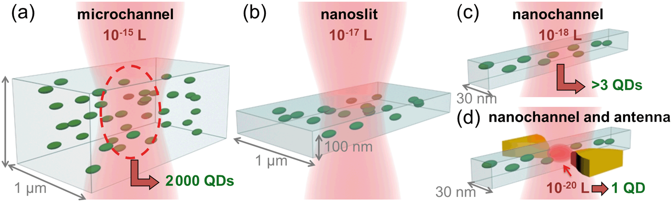 | ||
| Fig. 1 The volume and number of nanoparticles excited by a diffraction limited spot is illustrated for a microchannel, nanoslit, nanochannel, and nanochannel with a plasmonic nanoantenna. (a) A microchannel represents a system where the liquid is confined, but the effective volume is still larger than the focused laser spot. The typical volume is in the order of 10−15 L. (b) In a nanoslit, the depth is smaller than the laser spot, but both lateral dimensions are still diffraction limited. This system is comparable to a total internal reflection fluorescence (TIRF) microscope, and has excitation volumes of 10−17 L. (c) A nanochannel has two dimensions in the nanometric range, which are smaller than the laser spot, decreasing the volume to 10−18 L. (d) A plasmonic nanoantenna nanofocusing the light inside the nanochannel reduces the volume of investigation down to 10−20 L, and is not limited by diffraction anymore. | ||
Device description and fabrication
The concept and the configuration of the sensor and images of the different parts are shown in Fig. 2. The device (a) has a nanochannel, 30 nm wide by 30 nm deep, several microns long, running through the 35 nm gap of a gold bowtie nanoantenna (b); the antenna and the nanochannel are both in the same plane and perfectly aligned to each other as shown in the cross-section in (c), so the hot spot is entirely inside the nanochannel, as confirmed by finite difference time domain (FDTD) simulations (h). Two U-shaped microchannels (20 μm wide, 2 μm deep) deliver the liquid from the inlet reservoirs into the nanochannels. 3D funnel-like tapered inlets connect the micro and the nanostructures, minimizing the entropic barrier due to their size mismatch. These tapered inlets are particularly important for flowing long biomolecules (such as DNA) and avoid clogging. Scanning electron microscopy (SEM) images of the micro and nanofluidic parts and of the antenna can be seen in (d–f), and a photo of the all-transparent, polymeric device in (g). Further integration of other active microfluidic elements would be straight forward in future work: filters, sorters, mixers, integrated pumps, and on-chip fuel cells17–19 would make the device fully portable and allow for the study of (bio)molecules at relevant physiological concentrations in their native media with minimal alteration.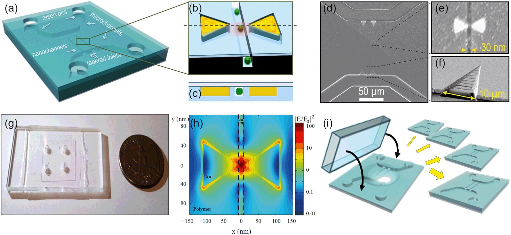 | ||
| Fig. 2 Device concept and images. (a)–(c) show a scheme of the device: a nanochannel is integrated with a plasmonic bowtie nanoantenna; the nanochannel has similar dimensions to the antenna gap and runs perfectly aligned and level to it. The nanochannel is integrated in a complete microfluidic system, for total analyte and liquid control. (d)–(f) show SEM images of the different structures in the device: the microchannels, the gold plasmonic bowtie nanoantenna aligned to the nanochannel and the 3D tapered inlets respectively. (g) Shows a photo of a functional device with four holes for liquid input and bonded to a coverslip. (h) is an FDTD simulation of the |E/E0|2 for a plasmonic bowtie nanoantenna embedded in polymer and with a nanochannel running along the gap in resonance conditions (λ = 870 nm). The field enhancement and confinement at the gap (inside the channel) can be observed. (i) Shows a scheme of the devices fabrication by nanoimprint lithography, which allows for parallel replication of the multilevel, multifunctional devices in just one step, 30 seconds long, without further post-processing or pattern etching. | ||
We have developed a unique process for device fabrication, compatible with mass production. The multilevel, multidimensional channels are patterned in a UV-curable polymer20,21 in a single, 30 second long, imprinting step22 by direct UV nanoimprint lithography (UV-NIL)23 (Fig. 2(i)). Nanoimprint lithography24,25 is a cost-effective and high resolution approach in place of solely photo- and electron beam-lithography methods, which lack sufficient resolution or reasonable throughput. As an added advantage, multiple depth levels, with different dimensions and 3D structures are all imprinted simultaneously. After imprinting the fluidic circuits, the nanoantennas are defined by selectively filling the two triangles adjacent to the nanochannels with gold by shadow deposition of a sacrificial layer and lift-off. The resulting antennas (Fig. 1(e)) are self-aligned to the nanochannel and are made of pure gold without an adhesion layer, which are well known to quench the field enhancement.26–28 A thin polymer wall of 1–2 nm separates each triangle tip from the nanochannel to avoid direct contact between the liquid and the metal. This prevents contamination and makes the device reusable. In addition, this wall ensures a good metal lift off; otherwise, when the triangles are merged with the nanochannels, we systematically observe gold remaining at the gap after the lift off, resulting in merged antennas. The devices are finally sealed by bonding to a glass coverslip, to confine the liquid inside the fluidic circuitry. The whole process is parallel and performed at wafer scale, which reduces fabrication costs and enables high yield and reproducible devices. The different steps of the fabrication process, including the fabrication of the silicon master mold, are detailed in the ESI.† Also, the different device configurations and channel layout used for the different measurements of this work are described and shown there.
Liquid confinement, flow, and stretching of DNA molecules
To prove the physical confinement of liquid into the nanochannels and the continuity of the flow, single DNA molecules (λ-DNA, 48502 base pairs, stained with YOYO-1) in an aqueous buffered solution were driven into and stretched along the nanochannels by electrophoresis. Fig. 3(a) shows a time sequence of the molecules flowing from one microchannel to the other by passing through a 25 nm wide, 27 nm deep nanochannel. A sketch of the geometry of these channels is also shown for reference. The molecules spontaneously enter the tapered inlet region, and are driven through the nanostructures when a voltage drop is applied between the opposite microchannels. By varying the voltage and its polarity, the molecules can be manipulated. The measured length of the stretched molecules in the 25 nm × 27 nm nanochannels is 18.7 μm, which is very close to its contour length of 21.8 μm.29 This value is larger than that obtained for similar molecules stretched in glass nanochannels, not only confirming their actual confinement, but also suggesting a strong charging of the polymer walls.30 More details about these characterizations and the length analysis of the stretched molecules in 150 μm long nanochannels can be found in the ESI† and attached videos.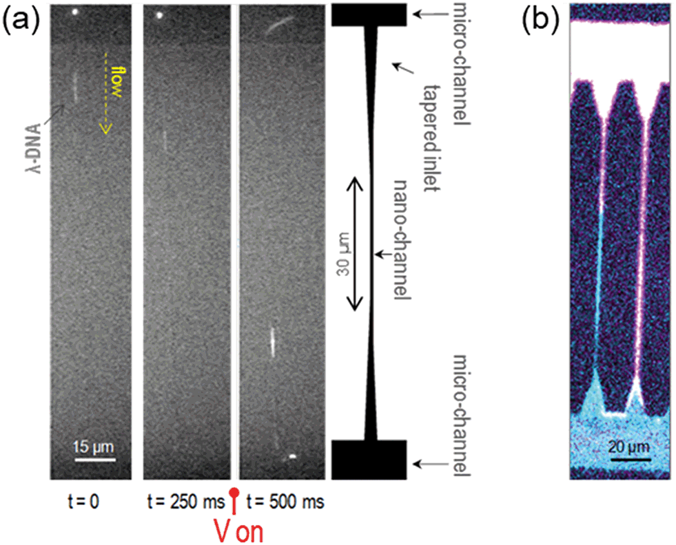 | ||
| Fig. 3 Flow and liquid confinement in the nanochannels. (a) Fluorescence images of individual molecules of λ-DNA flowing along a 25 nm × 27 nm nanochannel. The molecules enter the channel, and are driven trough as the voltage, V, is turned on (Von). A sketch of the nanochannel geometry is shown on the right to facilitate the visualization. (b) Liquids stained with different fluorophores were flown into the device by capillary action; DI water stained with Rhodamine 6G is shown in pink in the image, filling the upper microchannel and going along the nanochannels. The image was obtained with a laser scanning confocal fluorescent microscope. These nanochannels are 150 μm long. | ||
To test the flow of other liquids and the polymer resistance against solvents, different liquids (like hexane, toluene, isopropanol and acetone) stained with different fluorophores were flown into the device and imaged by confocal fluorescence microscopy, as shown in Fig. 3(b). In the ESI† we show spatially resolved micro-spectroscopy measurements to check the sealing quality and the confinement of the liquids into the channels and to discard leaks.
Resonance shift
The plasmonic antennas resonate in the range of 700–850 nm as measured by dark field scattering spectroscopy. The position of the localized surface plasmon resonance (LSPR) peak of the antennas depends on the specific antenna, its geometry, gap, and metal thickness. A typical dark field resonant signal of an antenna integrated with a nanochannel can be seen in Fig. 4(a), blue line. Interestingly, the resonance also depends on the refractive index of the media between the triangle tips, what can be exploited for high sensitivity sensing of the material inside the channel. We have observed how the liquid inside the nanochannel causes a resonance shift for toluene (n = 1.497) as shown in Fig. 4(a), black line. The exact peak positions are shown in Table 1. The measured shift for toluene is 45.5 ± 0.5 nm, and thus, the sensitivity of the system is 91 nm RIU−1. The liquid volume that is causing the shift is just the 30 zeptoliters in the antenna gap, which shows the sensitivity and capabilities of the device. Sensing by dark field resonance nano-spectroscopy can be exploited in future works to study local changes inside the nanochannel, associating the refractive index change to molecular adsorption for example in immunosensing assays,31 confined chemical reactions, local density changes, and other phenomena that are typically observed by surface plasmon resonance (SPR) (bio)sensing.32–34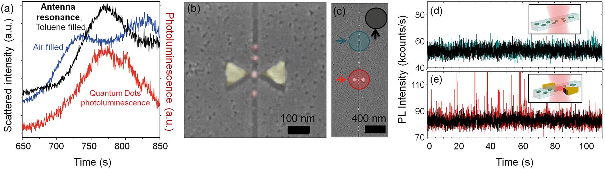 | ||
| Fig. 4 Detection of discrete emitters (quantum dots) one by one. (a) Spectra of the photoluminescence of the quantum dots used for the experiment (red line), compared to the resonant peak of the nanoantenna when the channel is empty (blue line) and when the channel is filled up with toluene (black line) – which is the media where the quantum dots are suspended. The dark field measurements were obtained with linearly polarized light along the antenna axes. (b) and (c) are SEM images of the quantum dots in the nanochannel and at the nanoantenna gap. The images were obtained after the optical experiments, by removing the glass coverslip, so the quantum dots got dry and stayed immobile inside the nanochannels. In (c) we marked the approximate spots where the photoluminescence signals were recorded. (d) and (e) show photoluminescence signals recorded along time for the laser fixed at a nanochannel without antenna (d), blue line, and at the same nanochannel with a bowtie nanoantenna (e), red line; both signals are compared against the background (black line). In (e), the background was vertically displaced to match the signal for a better visualization. The peaks corresponding to single quantum dots are very clear in (e), while difficult to resolve in (d). The graphs in the figure were obtained with a laser power of 40 μW. | ||
| Material in the nanochannel | Peak position (nm) | Shift (nm) | Sensitivity (nm RIU−1) |
|---|---|---|---|
| Air (n = 1) | 728.0 ± 0.4 | — | — |
| Toluene (n = 1.497) | 773.5 ± 0.3 | 45.5 ± 0.5 | 91 |
Two-photon photoluminescence characterization
Plasmonic antennas enhance the optical fields more efficiently than flat metal surfaces. This enhancement is on the order of 104 for our bowtie-shaped antennas, as we have quantified by comparing the two-photon photoluminescence (TPPL) signal between a 35 nm gap nanoantenna and a non-structured, flat gold surface on the same sample (see ESI†). The enhancement obtained for the polymer-embedded structures is higher than that of an antenna patterned on top of a flat substrate at air.35 FDTD simulations (Fig. 2(h)) show that the polymer surrounding the metal (which has a refractive index n = 1.520) pushes the optical fields into the lowest refractive index zone (i.e., the nanochannel). This results in better confinement compared to a similar antenna with the same tip-to-tip separation at air.Single, individual quantum dots detection
The sensor can also be used to detect and quantify discrete fluorescent emitters in real time. Plasmonic nanoantennas are excellent for high-contrast excitation of fluorophores since they enhance and confine the optical fields in the gap when illuminated within their resonant frequency range.13,36–41Quantum dots (QDs) have been flown into the device to show its potential for single emitter quantification even at ultra-high concentrations. Quantum dots are frequently used in biological experiments as point markers, and their individual detection opens the route for a variety of applications. We have used core/shell CuInS/ZnS quantum dots dispersed in toluene, with an emission maxima at λ = 780 nm. The PL emission of the QDs overlaps with the resonance of the nanoantenna when the channel is filled up with toluene, as shown in Fig. 4(a). The graph in the figure compares the resonance of an antenna when the nanochannel is empty (blue line), and when it is filled up with toluene (black line), and both spectra are shown together with the measured PL emission from the quantum dots (red line). The measurements were obtained with linearly polarized light along the antenna axes. The quantum dots have an average diameter of 8 nm and the nanochannels are 30 nm deep by 30 nm wide, enabling single file delivery. This can be seen in the SEM images in Fig. 4(b) and (c), which were obtained after the optical characterization of the devices. The QDs were used in a concentration of 25 mg mL−1. At this concentration, there would be more than 2000 quantum dots excited in a diffraction-limited spot (see calculations in the ESI†), as sketched in Fig. 1(a), making their individual detection extremely difficult using standard detection systems.
As the quantum dots flew along the nanochannels, a laser (λex = 633 nm) was focused at different spots of the sample and the photoluminescence (PL) signal recorded in real time with a single photon counter. Fig. 4(d) and (e) show PL time traces obtained when the laser was focused at the nanochannel (d) and at the same nanochannel in a section with an antenna (e), as marked in Fig. 4(c). In both cases, the measurements were obtained under the same conditions, just by moving the laser few microns with a piezoelectric stage as described in the ESI.† Both signals are compared against the background, recorded by focusing the laser on a flat, featureless surface of the sample.
The time traces differ dramatically: the quantum dots can be individually detected, one by one, as they pass through the nanoantenna gap, while they are hardly visible without it. Fig. 5(a) and (b) shows two exemplary peaks from the nanochannel and antenna scans respectively, where the differences are evident. Without the antenna, the peaks are long in duration and hardly distinguishable from the background. With the antenna, single, sharp, narrow peaks corresponding to individual nanoparticles can be clearly seen. In addition, the peaks from the antenna scans have a “base-peak”, corresponding to the signal emitted as a quantum dot flows trough the non-enhanced section of the diffraction limited spot. It is noticeable that the intensity and duration of these base signals and those from the nanochannel without antenna are similar, as expected.
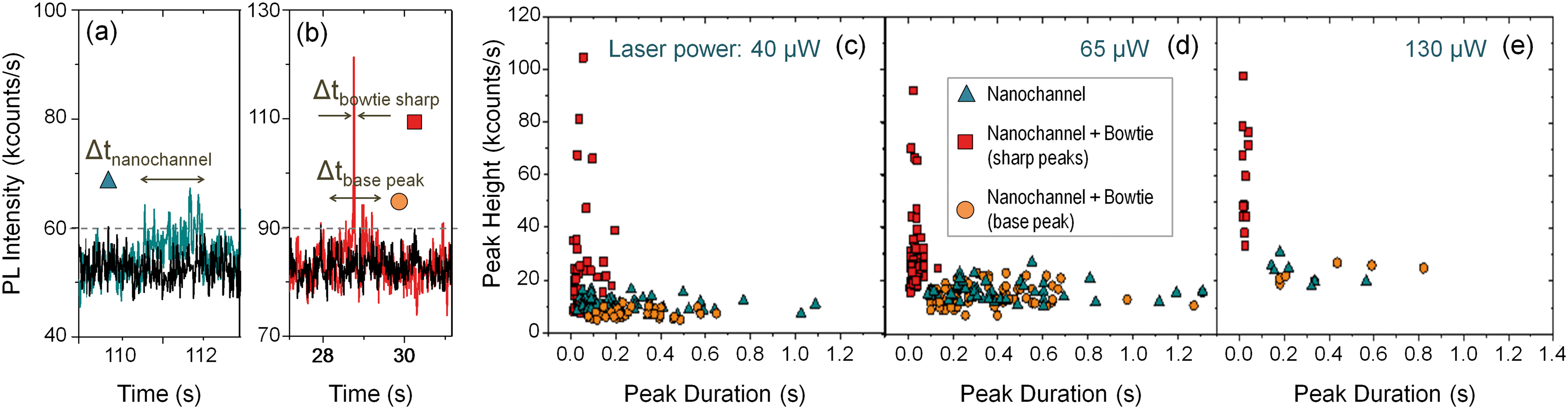 | ||
| Fig. 5 (a) and (b) Exemplary peaks obtained for a nanochannel and the same nanochannel with a bowtie antenna respectively, excited with 40 μW laser power. (c) Scattering plot where the duration of each peak has been plotted against its height for peaks obtained at the nanochannels (blue dots), and at the antenna (orange and red dots). The red dots show the data for the sharp, narrow peaks, corresponding to the QDs passing trough the antenna gap. The orange dots correspond base peaks that can be often observed for the antenna scans. (d) and (e) Show similar plots, obtained with different laser powers of 65 μW and 130 μW respectively. The vertical axes are cut at 120 kcounts per s to facilitate the visualization, even if some points have higher heights. | ||
These results prove that the nanoantenna is a key component for two main reasons. The first is that it clearly enhances the raw photoluminescence emission, for a better signal-to-background ratio. This level of sensitivity allows for a reduced excitation power, and real-time observation of particle flow due to the shorter integration time required for data acquisition. The second and most important one is that it allows for the observation of single, individual particles independent of their concentration (high or low) due to the nano-focusing of the signal into the 30 nm gap. This is crucial for quantification of the sample concentration.
Dependence on the excitation conditions
The dynamic flow of the quantum dots was recorded using different excitation powers. The minimum power from which the PL signal from the quantum dots passing through the plasmonic hot spot is detectable is 4 μW; at 40 μW the PL signal is detectable even without the antenna; and at around 150 μW the gold antennas melt and lose their shape. Fig. 5(c) shows a scattering plot where the height (i.e., PL intensity) of each peak has been plotted against its duration (Δt) for different time scans obtained with 40 μW excitation power. We differentiate three types of peaks: those obtained at a nanochannels (in blue), the narrow sharp peaks from the antenna (in red) and the base peaks from the antenna signals (in orange). The marks from the antenna peaks are scattered around 0.05 s duration for this laser power, and are spread at intensities higher than 20 kcounts per s. The marks from the nanochannel peaks and antenna base peaks are scattered along longer times, and have lower intensities, below 20 kcounts in all the cases. Fig. 5(d) and (e) show similar plots for scans obtained at 65 μW and 130 μW excitation powers respectively. Higher excitation powers increase the PL signal from both, the antenna and the nanochannel peaks.Fig. 6(a) shows histograms of the emitted PL intensity of quantum dot signals obtained at the same nanoantenna for several different excitation powers. And Fig. 6(b) shows the dependence of the PL emission on the excitation laser power as derived from the histograms. The average raw enhancement factor (Iant,av/Inch) is in the order of 4×, and the maximum enhancement that we observed is Iant,max/Inch = 14.3, where Inch and Iant,av are the averaged intensity of the signals measured at the nanochannel and at the antenna respectively, and Iant,max is the intensity of the highest peak measured with each laser power. The different values for the enhancement factors are summarized in Table 2.
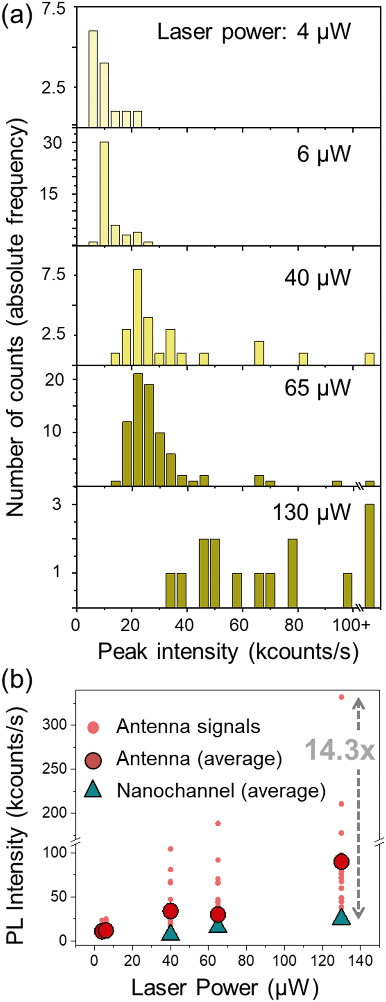 | ||
| Fig. 6 (a) Histograms showing the number of peaks with a certain PL emission intensity for different excitation powers. The histograms were obtained using a binning size b = 4, and a sampling size of 13, 45, 26, 79 and 15 respectively. (b) Dependence of the emitted intensity on the excitation power for quantum dots flowing along a nanochannel (blue markers) and in a nanochannels with a plasmonic antenna (red markers). The intensity of every peak has been plotted (small, light red circles) to show the scattering of the signals, together with the average value for each laser power (big, dark red circles). | ||
| Excitation power (μW) | PL signal from quantum dots | ||||
|---|---|---|---|---|---|
| Nanochannel, Inch | Nanochannel with antenna Iant | ||||
| Average (counts) | Average intensity Iant,av (counts) | Average enhancement Iant,av/Inch | Maximum intensity Iant,max (counts) | Maximum enhancement Iant,max/Inch | |
| 4 | — | 10.7 | — | — | — |
| 6 | — | 12.3 | — | — | — |
| 40 | 8.5 | 34.3 | 4.0 | 104.5 | 12.2 |
| 65 | 15.4 | 30.3 | 2.0 | 188.4 | 12.2 |
| 130 | 23.1 | 95.3 | 4.1 | 332.0 | 14.3 |
We believe that a higher enhancement factor could be achieved following some improvements. For example, by coupling not only the emission from the quantum dots to the optimal spectral range of the antenna, but also the wavelength of the excitation laser, the enhancement would be higher. Having a photon counter with faster binning capabilities would better match the fast speed of the quantum dots in the nanochannels to increase the photons captured per bin. In addition, it should be taken into account that the antenna also enhances the autofluorescence from the polymer, and emits some broadband signal,42 so the background increases when we measure at the antenna compared to the bare nanochannels (see Fig. S10†), what buries the PL signal from the quantum dots, affecting the enhancement factor that we report.
The duration of the peaks measured at the antennas, Δt, is in the order of tens of ms, as shown in Fig. 5(b–d). The histograms in the ESI† show that the peak duration depends on the excitation power to some extent. The typical peak duration is between 20 and 30 ms, but a significant number of peaks with longer duration appear for intermediate laser powers as can be seen in the histograms in the ESI.† Increasing the power increases the duration of some peaks, likely due to optical trapping effects. But powers higher than 40 μW have the opposite effect, due to localized heating, leading to higher particle mobility,43,44 thus reducing the peak duration.
Quantification of individual quantum dots at ultra high concentrations
As a proof of concept for single emitter quantification even in the extreme case of high concentrations, when several particles populate the diffraction limited spot, we show the quantification of the quantum dots. For the concentration used here, 25 mg mL−1, there would be more than 2000 quantum dots excited simultaneously by a diffraction limited spot in a non-confined liquid, as schematized and shown before in Fig. 1 and discussed in the calculations in Table S1 in the ESI.† A microchannel (Fig. 1(a)), a nanoslit (b) or a nanochannels (c) would reduce the number of excited particles. But for such a high concentration as used here, even in a nanochannel as small as 30 nm wide, 30 nm deep there would be still an average of three quantum dots simultaneously excited. The SEM images of Fig. 4(b) and (c), which were obtained by unbonding the sample after the experiments with a concentration of 25 mg mL−1, confirm that still several quantum dots (between two and five, as observed in the images) are present in the nanochannels, inside the diffraction limited spot, in agreement with the calculations. The antenna combined with the nanochannel (Fig. 1(d)), reduces the excited volume in five orders of magnitude compared to the initial diffraction limited spot. And only in this case is it possible to unequivocally observe one emitter at the time.Thanks to the simultaneous confinement of light and liquid, the nanoparticles can be counted one by one for a given time interval to obtain their concentration, [C], in real time. We estimated the volumetric liquid flow rate, Q, by Q = VQD/Δt where Δt is the duration of the luminescence peaks and VQD is the volume of the quantum dots. Knowing the flow rate Q, and counting the number of peaks per minute, n, we calculated the concentration by [C] = n·ρ·VQD/Q, where ρ is the average density of the quantum dots. Fig. 7 shows the concentration of quantum dots obtained for several measurements with different laser powers. For powers <16 μW, the measured concentration is lower than the expected one (given by the provider), as can be seen in the graph, probably because some peaks are not distinguishable from the background and do not pass the intensity threshold that we set for their quantification. For powers ≥16 μW we typically count between 10 and 20 peaks in 60 seconds long scans. With this, we obtain a concentration of [C] = 29.1 ± 0.9 mg mL−1, as averaged from the different measurements obtained with laser powers ≥16 μW. This value compares with the one given by the provider, 25 mg mL−1. Solvent evaporation during the measurements can account for the higher concentration that we measure with the devices.
 | ||
| Fig. 7 Measured concentration of quantum dots, obtained by counting the peaks, one by one, as they pass trough the antenna gap. The concentration was measured for different laser powers; the value obtained for low laser powers (<16 μW), is lower than the expected one. The concentrations obtained from the measurements using laser powers ≥16 μW lie within the range of 29.1 ± 0.9 mg mL−1. They are reproducible and comparable to the value given by the provider, 25 mg mL−1, marked in the plot in the figure for reference. | ||
Since the sensor counts single particles, low concentrations can be measured in the same way by counting peaks over longer time scans. The throughput can be improved by integrating a larger number of channels in parallel. In the devices fabricated for this work we have tens of nanochannels with their corresponding nanoantennas, and a larger number would require little extra processing effort. These quantification results show how we can break the concentration barrier and count nanoparticles one by one even at ultra high concentrations in a standard, diffraction limited microscope, using our nanoimprinted devices.
Because the detection of quantum dots is in principle compatible with their functionalization, the sensor has direct application in counting quantum dot-labeled single-(bio)molecules at any concentration, in detecting barcoded DNA,45,46 in virus identification,47 or in single protein analysis.48 In addition, the device operation is easily extended for the detection other types of fluorophores and single emitters, allowing for flexibility and versatility in (bio)chemical functionalization.
Conclusion
In summary, we have presented an integrated device that simultaneously confines light and liquid by integrating a 30 nm × 30 nm nanochannel with a 35 nm gap plasmonic bowtie nanoantenna. The plasmonic antenna provides the signal enhancement and sensitivity necessary for single molecule detection, and the nanochannel confines the liquid and is used to control and deliver the analyte exclusively through the sensitive hot spot. Since the dimensions of the channel can be accurately defined, it can be tailored for in-line single (bio)molecule or nanoparticle delivery. A reliable, low-cost wafer-scale fabrication technology has been developed, based on nanoimprint lithography, for integrating the fluidic and the plasmonic components without unnecessary lithography and alignment steps. The integrated device is a powerful tool to study phenomena in liquids confined in 10−21 L in real time. As an example we have measured a shift of 45 nm on the resonance peak when the nanochannel is filled by toluene, compared to the empty channel. In addition, the device can be used to detect and count individual nanoparticles even at ultra high sample concentration in their native media with minimal manipulation. For the same excitation power, the quantum dots flowing along the nanochannel are observed in groups, and the signal is hardly distinguisible from the background. For the nanochannel with the antenna, the peaks become sharp and intense, corresponding to individual nanoparticles flowing one by one along the nanofocused spot. Thanks to this, the sample concentration can be measured in real time, just by counting the number of peaks per time interval, just using a standard, diffraction limited set up.Methods
Sample fabrication
Ormostamp and Ormocomp (both commercially available from micro resist technology GmbH) were used as functional materials to pattern the fluidic devices. These are UV-curable hybrid polymers, that were chosen because of their minimal shrinking after curing, long term stability and resistance to solvents. The exposure was done at λ = 365 nm, with a 13 mJ lamp, for 30 seconds.Nanochannel design and geometry
Different stamps with different nanochannel configurations were used. Flowing liquids, and especially molecules into such small 30 nm × 30 nm nanochannels is very challenging, we facilitate the task by adding tapered transient inlets, triangular or squared, depending on the specific use of the sample. To flow DNA, we used very long, homogeneous nanochannels, with large, triangular, 3D inlets at the entrances. These (150 μm) nanochannels were long enough that we could see the DNA completely stretched inside and measure its contour length. But the flow inside is usually very difficult, and the voltage needed is very high, what creates bubbles and makes the experiments short. For this reason, we made a different set of stamp and samples, were the nanochannel, 30 nm × 30 nm was 5 μm long. These were connected to very long (50 μm) 2D tapered inlets, to make the flow faster. For the quantum dots, inlets with different depth levels were used. The details of the different devices are shown in the ESI.†DNA sample preparation
We used commercial double stranded DNA from the λ-bacterio-phage (λ-DNA) from New England Biolabs. The molecules were stained with the intercalating dye YOYO-1 (from Invitrogen), in a ratio of 5![[thin space (1/6-em)]](https://www.rsc.org/images/entities/char_2009.gif) :1 basepairs per dye. In this conditions, the molecules have a contour length of Lλ = 21.8 μm. The DNA was diluted in a TBE/TAE buffered solution, down to a concentration of 100 ng mL−1. The molecules were driven into the nanochannels by electrophoresis. Platinum electrodes were immersed inside the reservoir holes. A voltage difference of 80 V was applied between the two opposite microchannels, so the molecules were forced to flow through the nanochannels.
:1 basepairs per dye. In this conditions, the molecules have a contour length of Lλ = 21.8 μm. The DNA was diluted in a TBE/TAE buffered solution, down to a concentration of 100 ng mL−1. The molecules were driven into the nanochannels by electrophoresis. Platinum electrodes were immersed inside the reservoir holes. A voltage difference of 80 V was applied between the two opposite microchannels, so the molecules were forced to flow through the nanochannels.
Imaging
Scanning electron microscope images of the samples were obtained with a Zeiss Ultra 60-SEM. Wide field epi-fluorescence images of the DNA molecules in the nanochannels were obtained in an inverted microscope, Olympus IX-81, using a 100×, water immersion objective, with an Andor EMCCD Camera. The laser scanning confocal microscopy images were obtained with a Zeiss 710 Laser Scanning Confocal Microscope.Dark field spectroscopy
Dark field spectroscopy measurements were done using a 100× air objective, with a numerical aperture of 0.95, and an oil immersion condenser, with a numerical aperture of 1.45. The output signal was spatially filtered by using a 100 μm pinhole, so only the scattering from a 1 μm circular area was recorded. This signal was analyzed with a spectrometer, integrating 10 times, 1 second spectra. The scattering signal from the antenna was divided by the lamp signal to obtain the relative scattering. In some cases, when there was a strong background, this was also recorded on a non-structured area, close by the region of interest with the antenna, and further subtracted. The excitation was done using a broad emission lamp, and a polarizer was used to excite the antennas either parallel or perpendicular to their main axes.Real time photoluminescence (PL) measurements
An inverted microscope was modified to allow for laser excitation. The sample holder was mounted on a piezoelectric scanner to control the laser position and allow for confocal imaging and for spatially resolved spectroscopy. At the output, there were three ports for signal analysis: a camera, a spectrometer, and an avalanche photodiode (APD) for spatially resolved measurements and intensity timed scans.Time scans of the quantum dots were performed using a 633 nm He:Ne laser. A 633 nm long pass filter was used to cut the excitation signal. The luminescence was recorded with an avalanche photodiode. Several different laser excitation powers were used, from 5 μW up to 200 μW. The light was not polarized.
We used CuInS/ZnS quantum dots dispersed in toluene from Ocean Nanotech. The quantum dots emit at λ = 780 nm as measured with the spectrometer. The average total size of the nanocrystals is around 5 nm for the inorganic part, plus a 2–3 nm thick organic stabilizing layer. The dimensions of the dots were obtained from the provider and confirmed by SEM. All the results about QDs shown in the text were obtained with these nanocrystals.
The density of the quantum dots, necessary to calculate the concentration by counting the number of peaks per second, was calculated taking into account its different layers with their different densities. We calculated and added the mass of each part, and divided it by the QD total volume. For this, the CuInS core was set to a diameter of Φcore = 4 nm with ρCuInS = 4.73 g cm−3, the ZnS shell Φshell = 1 nm with ρZnS = 4.09 g cm−3, and the organic coating, dodecanethiol, as Φcoating = 2 nm with ρdodecanethiol = 0.85 g cm−3.
Author contributions
I. F. C. and S. C. designed and planned the research. I. F. C., M. W. and E. M. performed the experiments. A. S. helped with the optical set up. All authors discussed the results. I. F. C., M. W. and S. C. wrote the paper.Conflicts of interest
The authors declare no competing financial interest.Acknowledgements
NSF SBIR program is acknowledged for partial funding, Award ID 1315550. I. F. C. acknowledges the European Union, FP7 People: Marie-Curie Actions (PIOF-GA-254498) for support. The work at the Molecular Foundry was supported by the Office of Science, Office of Basic Energy Sciences, of the U.S. Department of Energy under Contract No. DE-AC02-05CH11231.References
- K. W. Y. Chan, et al., MRI-detectable pH nanosensors incorporated into hydrogels for in vivo sensing of transplanted-cell viability, Nat. Mater., 2013, 12(3), 268–275 CrossRef CAS PubMed.
- D. A. Stuart, et al., In Vivo Glucose Measurement by Surface-Enhanced Raman Spectroscopy, Anal. Chem., 2006, 78(20), 7211–7215 CrossRef CAS PubMed.
- E. K. Wujcik, et al., Antibody nanosensors: a detailed review, RSC Adv., 2014, 4(82), 43725–43745 RSC.
- M. Swierczewska, et al., High-sensitivity nanosensors for biomarker detection, Chem. Soc. Rev., 2012, 41(7), 2641–2655 RSC.
- C. Escobedo, et al., Quantification of ovarian cancer markers with integrated microfluidic concentration gradient and imaging nanohole surface plasmon resonance, Analyst, 2013, 138(5), 1450–1458 RSC.
- A. Vergara, et al., An RFID reader with onboard sensing capability for monitoring fruit quality, Sens. Actuators, B, 2007, 127(1), 143–149 CrossRef CAS.
- M.-I. Baraton and L. Merhari, Advances in Air Quality Monitoring via Nanotechnology, J. Nanopart. Res., 2004, 6(1), 107–117 CrossRef CAS.
- J. Li, et al., Carbon Nanotube Sensors for Gas and Organic Vapor Detection, Nano Lett., 2003, 3(7), 929–933 CrossRef CAS.
- N. A. Jeffrey, et al., Biosensing with plasmonic nanosensors, Nat. Mater., 2008, 7(6), 442–453 CrossRef PubMed.
- A. G. Brolo, Plasmonics for future biosensors, Nat. Photonics, 2012, 6(11), 709–713 CrossRef CAS.
- J. A. Schuller, et al., Plasmonics for extreme light concentration and manipulation, Nat. Mater., 2010, 9(3), 193–204 CrossRef CAS PubMed.
- L. Novotny and N. van Hulst, Antennas for light, Nat. Photonics, 2011, 5(2), 83–90 CrossRef CAS.
- D. Punj, et al., A plasmonic/‘antenna-in-box’/platform for enhanced single-molecule analysis at micromolar concentrations, Nat. Nanotechnol., 2013, 8(7), 512–516 CrossRef CAS PubMed.
- P. E. Sheehan and L. J. Whitman, Detection Limits for Nanoscale Biosensors, Nano Lett., 2005, 5(4), 803–807 CrossRef CAS PubMed.
- F. De Angelis, et al., Breaking the diffusion limit with super-hydrophobic delivery of molecules to plasmonic nanofocusing SERS structures, Nat. Photonics, 2011, 5(11), 682–687 CrossRef CAS.
- P. R. Nair and M. A. Alam, Performance limits of nanobiosensors, Appl. Phys. Lett., 2006, 88(23), 233120 CrossRef.
- J. P. Esquivel, et al., Fuel cell-powered microfluidic platform for lab-on-a-chip applications: Integration into an autonomous amperometric sensing device, Lab Chip, 2012, 12(21), 4232–4235 RSC.
- J. P. Esquivel, et al., Microfluidic fuel cells on paper: meeting the power needs of next generation lateral flow devices, Energy Environ. Sci., 2014, 7(5), 1744–1749 RSC.
- K. H. Rasmussen, et al., A device for extraction, manipulation and stretching of DNA from single human chromosomes, Lab Chip, 2011, 11(8), 1431–1433 RSC.
- A. Klukowska, et al., Novel transparent hybrid polymer working stamp for UV-imprinting, Microelectron. Eng., 2009, 86(4–6), 697–699 CrossRef CAS.
- A. Schleunitz, et al., Innovative and Tailor-made Resist and Working Stamp Materials for Advancing NIL-based Production Technology, J. Photopolym. Sci. Technol., 2013, 26(1), 119–124 CrossRef CAS.
- I. Fernandez-Cuesta, et al., Fabrication of fluidic devices with 30 nm nanochannels by direct imprinting, J. Vac. Sci. Technol., B: Nanotechnol. Microelectron.: Mater., Process., Meas., Phenom., 2011, 29(6), 06F801 Search PubMed.
- J. Haisma, et al., Mold-assisted nanolithography: A process for reliable pattern replication, J. Vac. Sci. Technol., B: Microelectron. Nanometer Struct.--Process., Meas., Phenom., 1996, 14(6), 4124–4128 CrossRef CAS.
- S. Y. Chou, P. R. Krauss and P. J. Renstrom, Imprint Lithography with 25-Nanometer Resolution, Science, 1996, 272(5258), 85–87 CrossRef CAS.
- H. Schift, Nanoimprint lithography: An old story in modern times? A review, J. Vac. Sci. Technol., B: Microelectron. Nanometer Struct.--Process., Meas., Phenom., 2008, 26(2), 458–480 CrossRef CAS.
- T. G. Habteyes, et al., Metallic Adhesion Layer Induced Plasmon Damping and Molecular Linker as a Nondamping Alternative, ACS Nano, 2012, 6(6), 5702–5709 CrossRef CAS PubMed.
- C. Jeppesen, N. A. Mortensen and A. Kristensen, The effect of Ti and ITO adhesion layers on gold split-ring resonators, Appl. Phys. Lett., 2010, 97(26), 263103 CrossRef.
- H. Aouani, et al., Crucial Role of the Adhesion Layer on the Plasmonic Fluorescence Enhancement, ACS Nano, 2009, 3(7), 2043–2048 CrossRef CAS PubMed.
- Y. Kim, et al., Nanochannel confinement: DNA stretch approaching full contour length, Lab Chip, 2011, 11(10), 1721–1729 RSC.
- C. Manneschi, et al., Stretching of DNA confined in nanochannels with charged walls, Biomicrofluidics, 2014, 8(6), 064121 CrossRef PubMed.
- T. Sannomiya, C. Hafner and J. Voros, In situ Sensing of Single Binding Events by Localized Surface Plasmon Resonance, Nano Lett., 2008, 8(10), 3450–3455 CrossRef CAS PubMed.
- A. A. Al Balushi, A. Zehtabi-Oskuie and R. Gordon, Observing single protein binding by optical transmission through a double nanohole aperture in a metal film, Biomed. Opt. Express, 2013, 4(9), 1504–1511 CrossRef PubMed.
- S. Zeng, et al., Nanomaterials enhanced surface plasmon resonance for biological and chemical sensing applications, Chem. Soc. Rev., 2014, 43(10), 3426–3452 RSC.
- J. Homola, S. S. Yee and G. Gauglitz, Surface plasmon resonance sensors: review, Sens. Actuators, B, 1999, 54(1–2), 3–15 CrossRef CAS.
- P. J. Schuck, et al., Improving the mismatch between light and nanoscale objects with gold bowtie nanoantennas, Phys. Rev. Lett., 2005, 94(1), 017402 CrossRef CAS PubMed.
- A. Kinkhabwala, et al., Large single-molecule fluorescence enhancements produced by a bowtie nanoantenna, Nat. Photonics, 2009, 3(11), 654–657 CrossRef CAS.
- K. Kneipp, et al., Ultrasensitive chemical analysis by Raman spectroscopy, Chem. Rev., 1999, 99(10), 2957–2976 CrossRef CAS PubMed.
- A. G. Curto, et al., Unidirectional Emission of a Quantum Dot Coupled to a Nanoantenna, Science, 2010, 329(5994), 930–933 CrossRef CAS PubMed.
- R. Regmi, et al., Nanoscale volume confinement and fluorescence enhancement with double nanohole aperture, Sci. Rep., 2015, 5, 15852 CrossRef CAS PubMed.
- A. Puchkova, et al., DNA Origami Nanoantennas with over 5000-fold Fluorescence Enhancement and Single-Molecule Detection at 25 μM, Nano Lett., 2015, 15(12), 8354–8359 CrossRef CAS PubMed.
- G. P. Acuna, et al., Fluorescence Enhancement at Docking Sites of DNA-Directed Self-Assembled Nanoantennas, Science, 2012, 338(6106), 506–510 CrossRef CAS PubMed.
- Y. Cheng, et al., Luminescence quantum yields of gold nanoparticles varying with excitation wavelengths, Nanoscale, 2016, 8(4), 2188–2194 RSC.
- A. Kotnala, D. DePaoli and R. Gordon, Sensing nanoparticles using a double nanohole optical trap, Lab Chip, 2013, 13(20), 4142–4146 RSC.
- A. Kotnala and R. Gordon, Quantification of High-Efficiency Trapping of Nanoparticles in a Double Nanohole Optical Tweezer, Nano Lett., 2014, 14(2), 853–856 CrossRef CAS PubMed.
- C.-Y. Zhang, et al., Single-quantum-dot-based DNA nanosensor, Nat. Mater., 2005, 4(11), 826–831 CrossRef CAS PubMed.
- A. Crut, et al., Detection of single DNA molecules by multicolor quantum-dot end-labeling, Nucleic Acids Res., 2005, 33(11), e98 CrossRef PubMed.
- C.-y. Zhang and J. Hu, Single Quantum Dot-Based Nanosensor for Multiple DNA Detection, Anal. Chem., 2010, 82(5), 1921–1927 CrossRef CAS PubMed.
- J. Chang and S. Rosenthal, Real-Time Quantum Dot Tracking of Single Proteins, in Biomedical Nanotechnology, ed. S. J. Hurst, Humana Press, 2011, pp. 51–62 Search PubMed.
Footnote |
| † Electronic supplementary information (ESI) available. See DOI: 10.1039/c9lc00186g |
| This journal is © The Royal Society of Chemistry 2019 |