
Air-stable mixed cation lead halide perovskite films and microscopic study of their degradation process†
Anubha
Agarwal
,
Shun
Omagari
 and
Martin
Vacha
*
and
Martin
Vacha
*
Department of Materials Science and Engineering, Tokyo Institute of Technology, Ookayama 2-12-1-S8-44, Meguro-ku, Tokyo 152-8552, Japan. E-mail: vacha.m.aa@m.titech.ac.jp
First published on 24th May 2023
Abstract
We report the preparation and nanoscale photophysical characterization of mixed cation perovskite films of the composition MA1−xFAxPbI3, with x = 0, 0.3 and 0.5. Films with x = 0.5 and 0.3 prepared in air using ethyl acetate as an antisolvent in a one-step spin-coating process are compositionally stable in ambient air for more than a year, in contrast to films prepared using a chlorobenzene antisolvent. The onset of degradation of the films near the film edges was monitored using in situ photoluminescence (PL) spectroscopy. The PL spectra of the degradation products are consistent with the PL spectra of 2D perovskite sheets of varying thicknesses. Morphologically, aging of the films brings about coalescing of the film grain structure into larger crystal grains. Furthermore, monitoring of the time traces of PL from individual nanoscale locations in the films (PL blinking) reveals that aging of the films does not change the extent of dynamic PL quenching or affect the observed long-range charge diffusion on the order of micrometers.
1. Introduction
Organic–inorganic hybrid perovskite solar cells (PSCs) have attracted considerable attention around the world owing to their excellent semiconducting properties. Progress in the power conversion efficiency improvement of solar cells has been very rapid, overcoming 25% efficiency1,2 in the last few years. The preparation of high-quality and long-term stable perovskite thin films is the key to obtaining highly efficient and environmentally stable perovskite solar cells. The commonly used technique for the fabrication of perovskite active layers is one-step spin coating, as the method is simple and easy to control. However, films often have incomplete surface coverage and poor morphology, which results in nonradiative recombination in solar cells. So far, solvent engineering including the use of antisolvents has been considered one of the most efficient ways to control the morphology and crystal structure of perovskite materials and obtain highly uniform perovskite films.3 A mixture of N,N-dimethylformamide (DMF) and dimethyl sulfoxide (DMSO) is a well-known polar solvent for the preparation of perovskite precursor solutions. The function of the antisolvent is to remove the high boiling-point solvent DMF and form a transparent intermediate (e.g., FAxMA(1−x)I–PbI2–DMSO) from its perovskite precursor solution, which leads to smooth and uniform perovskite films with fewer pinholes and with good optoelectronic properties.4At the same time, even the most uniform perovskite films have concerns with stability in ambient air. When the fabrication is carried out in an environment with the uncontrolled presence of humidity or air, the perovskite absorber layer is very sensitive to moisture and oxygen and can easily degrade as a result of high humidity either during the fabrication process or during device operation. To solve this problem, PSCs are being prepared mostly inside inert gas-filled gloveboxes to avoid humidity, which potentially increases the solar cell manufacturing costs.5 Therefore, research in the area of fabricating perovskite films in ambient air is highly desirable.6–8 In addition, most of the high-performance reported PSCs are based on toxic antisolvents, such as chlorobenzene, methylbenzene, diethyl ether or toluene, which is another major issue for the potential commercialization of PSCs. As a solution to both the above issues, the use of acetates including ethyl acetate (EA) as antisolvents9 has been proposed. EA features relatively low toxicity and low boiling point. During the formation of perovskite grains from the precursor solution under ambient conditions, high moisture resistance of acetates can reduce pinholes and achieve complete coverage on the substrate, forming high-quality perovskite films.7
So far, great effort has been focused on the improvement of the stability of PSCs by the choice of charge-transporting materials, perovskite compositional engineering or the use of a wide array of additives.10,11 On the other hand, less attention has been paid to the long-term ambient stability of perovskite films themselves. In terms of compositional engineering, mixed cations, MA1−xFAxPbI3 with x between 0.3 and 0.8, have shown increased stability due to optimized tolerance factor.12 Furthermore, the use of EA antisolvent has also been shown to increase the stability of perovskite films in ambient humidity.6 Using these approaches, stability of 80 days for devices without encapsulation in ambient air with controlled humidity has been demonstrated.13
Here, we report the preparation of mixed cation perovskite films in air with long-term stability and characterization of their degradation process by photoluminescence (PL) microscopy and spectroscopy over extended periods of time. PL microscopy has been a powerful tool to reveal the relationship between the nanoscale structure and properties in a variety of perovskite materials,14 including films15–18 and micro-/nanocrystals.19,20 We show that MA1−xFAxPbI3 films with x of 0.3 and 0.5 prepared in air using EA antisolvent are compositionally stable in ambient air for more than a year. The onset of degradation in these films is characterized by in situ PL spectra, which reveal the emission of decomposition intermediates.
2. Results and discussion
MA1−xFAxPbI3 films with x = 0, 0.3 and 0.5 were prepared on a PEDOT–PSS layer using one-step spin coating followed by the application of an antisolvent, as reported before.15 The antisolvent application step was optimized with respect to the deposition time. Apart from the EA antisolvent, chlorobenzene (CB) was used as a reference. After annealing, the resulting film thickness was on the order of 450 nm. The films were kept under ambient conditions with air humidity ranging between 40% and 60% and in ambient light for prolonged periods of time. The films prepared 12 months ago, 9 months ago, and 6 months ago, as well as freshly prepared films, were then compared and their properties were examined. Fig. 1a shows photographs of the x = 0, 0.3 and 0.5 films (denoted as FA 0%, FA 30% and FA 50%, respectively) prepared using EA, and for comparison an FA 50% film prepared using CB, at different stages of aging. The remaining compositions prepared using CB are shown in Fig. S1.† The size of each sample in the figure is 24 × 24 mm. The FA 0% (EA) and the FA 50% (CB) films show a color change from brown to yellow after 6 months, and further color bleaching as aging proceeds. Compared to that, the FA 30% (EA) and FA 50% (EA) films retain their original brown color throughout the 12-month period. The effect of aging can be seen as a slightly lighter color pattern mainly near the edges of the films, but overall the films retain their original appearance.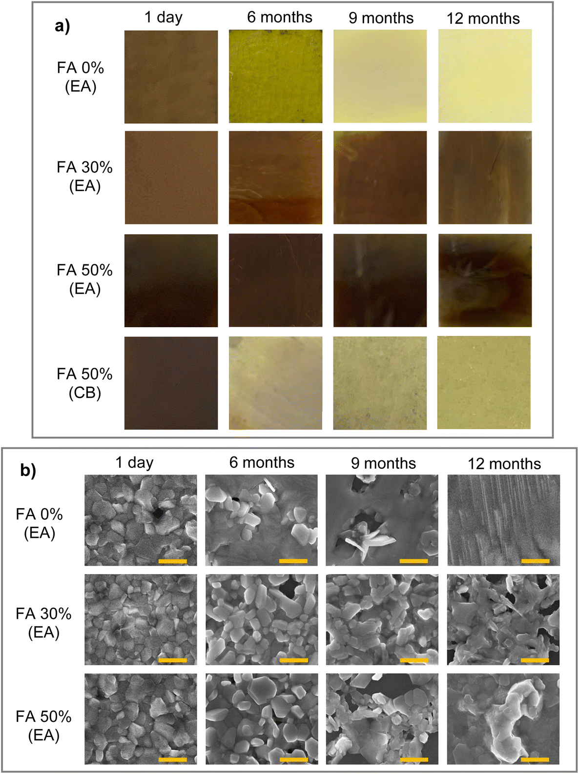 | ||
| Fig. 1 (a) Photographs of perovskite films prepared on a 24 × 24 mm microscope cover glass at different stages of aging from 1 day to 12 months. The perovskite compositions and antisolvent used are indicated in the figure (EA: ethyl acetate and CB: chlorobenzene). (b) SEM images of the perovskite films of different compositions prepared using EA antisolvent at the same stages of aging as in (a). The images are taken from the centers of the films, scale bars are 500 nm. | ||
To check the corresponding changes in the film morphology, we carried out SEM imaging near the center of the films for the FA 0% (EA), FA 30% (EA) and FA 50% (EA) samples, as presented in Fig. 1b. All fresh films show good crystal quality with very few pinholes, which is largely retained for the FA 30% (EA) and FA 50% (EA) samples after 6 months. In the FA 0% (EA) sample, the crystal morphology starts progressively disappearing even after 6 months, and the 12-month sample does not show any signs of the original film structure. Compared to that, for the FA 30% (EA) and FA 50% (EA) samples individual crystal grains appear to coalesce into larger ones, but the crystal morphology is still visible even after 12 months, especially in the FA 30% (EA) sample. In addition, UV-Vis absorption spectra of all the samples shown in Fig. S2† confirm the presence of perovskite absorption bands in all films during the aging process.
To study the effect of aging on the nanoscale compositional stability of the perovskite films, we carried out microscopic in situ PL spectroscopy of the samples. The PL is excited with a 442 nm laser and spectra are recorded from diffraction-limited size locations across the films. The results for the 12 month EA samples are shown in Fig. 2. Here, we measured and analyzed separately the center areas of the films (5 × 5 mm) and the areas close to the edges. The two types of locations are schematically indicated in the photographs of the films in Fig. 2a–c. For the FA 30% (EA) and FA 50% (EA) samples, the center areas show exclusively spectra corresponding to the mixed cation perovskite phase. Examples of such spectra at different locations in the film spanning more than 25 μm are plotted as 2D spectral plots (position vs. wavelength) in Fig. 2g and j. These plots show distributions of the PL peaks within the spectral range of the corresponding perovskite composition. Typical PL spectra exhibiting a single peak are shown in Fig. 2h and k. We further analyzed the spectral peak positions (by Gaussian fitting) for a statistical sample of locations and plotted their distributions as histograms in Fig. 2i and l, together with bulk PL spectra of the corresponding freshly prepared films. Both the FA 30% (EA) and FA 50% (EA) samples show broad distributions of the local PL spectral peaks, with the distribution maxima corresponding to the bulk PL spectral peaks. The distribution is broader for the FA 50% (EA) sample where it spans a range from 790 nm to 825 nm. This range covers the whole spectral range of all compositions from FA 0% to FA 100%, as reported before.15 This result is evidence of the local compositional heterogeneity of the films and means that the FA 50% (EA) samples contain purely MA domains (FA 0%-like spectra), purely FA domains (FA 100%-like spectra) and domains composed of mixed MA/FA cations of varying ratios. The wavelengths corresponding to the FA 0% and FA100% compositions are marked in the histograms by red lines. Compositional heterogeneity is found in the FA 30% (EA) films as well, but in this case the longest-wavelength components (corresponding to FA100%) are missing in the histogram. We have reported such compositional heterogeneity for freshly prepared samples before,15 and it is interesting to observe how the heterogeneity evolves with aging of the samples. Histograms of the PL peak positions for all three samples (FA 0% (EA), FA 30% (EA) and FA 50% (EA)) in the film center areas are shown in Fig. S3† at different stages of aging, i.e., from fresh to 6 months, 9 months and 12 months. Most interestingly, the wavelength ranges of the distributions for the FA 30% (EA) and FA 50% (EA) samples have not changed over the period of one year, and the shapes of the histograms at different times are also similar. This means that the samples (in their center areas) are compositionally stable for at least one year, and that there is no observable cation migration over this period that would change the shape of the histograms, shift their positions, or cause the appearance of the FA 100% components in the FA 30% (EA) samples.
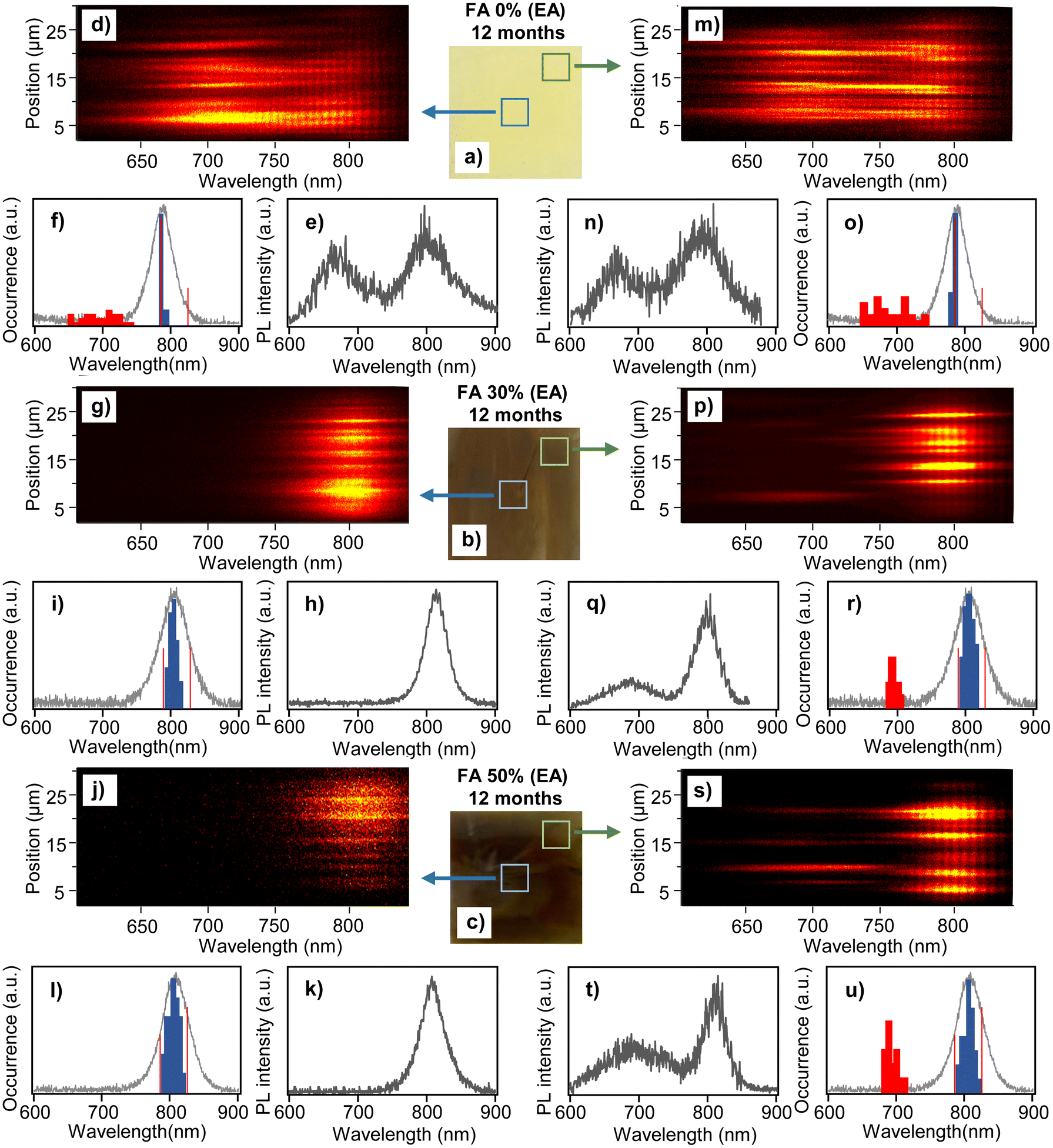 | ||
| Fig. 2 Spectroscopic characterization of the degradation process. (a)–(c) Photographs of perovskite films of different compositions as indicated in the figure taken 12 months after the fabrication of films. The squares and arrows indicate symbolically the areas used for spectral measurements. (d), (g) and (j) Representative 2D PL spectral plots (position vs. wavelength) for central locations in the respective films. (m), (p) and (s) The same plots for locations close to film edges. (e), (h) and (k) Examples of typical PL spectra taken in central locations of the respective films. (n), (q) and (t) The same PL spectra taken in locations close to film edges. (f), (i) and (l) Histograms of local PL spectral maxima (blue and red bars) measured in central locations of the respective films. The vertical red lines indicate the positions of the distribution peaks for the FA 0% and FA 100% samples. Bulk PL spectra of freshly prepared films of the respective composition are shown by solid grey lines. (o), (r) and (u) The same histograms obtained from spectra measured in locations close to film edges. | ||
PL spectral data for the center area of the 12-month-old FA 0% (EA) sample (which is apparently degraded in Fig. 1) are shown in Fig. 2d–f. The 2D spectral plots and the typical PL spectrum show peaks at around 785 nm corresponding to the pure MAPbI3 perovskite phase from all measured locations. This is a surprising result because in the film appearance and SEM images the sample looks completely degraded, but the UV-Vis absorption spectra (Fig. S2†) show weak perovskite absorption together with a band corresponding to PbI2. In addition, there are broader PL peaks with higher intensity, which are shifted to the blue region from the perovskite peaks. The histogram of the PL spectral peaks shown in Fig. 2f confirms a narrow distribution of the perovskite peaks at 785 nm and a broad distribution of the blue-shifted band which spans a range from 641 to 759 nm. We assume that the blue shifted PL originates from the products of the degradation process.
Similar features are observed in the PL spectra of all samples taken from the edges of the films. For the FA 30% (EA) and FA 50% (EA) samples (Fig. 2p–u), the main fraction in the PL spectra corresponds to the mixed cation perovskite phase. Distributions of these spectra are similar to those obtained from the center areas, and for the FA 50% (EA) sample they cover the whole spectral range of all mixed cation compositions. The blue-shifted spectra are distributed between 680 and 711 nm and their fraction is larger for the FA 50% (EA) sample. This result indicates that on microscopic scales there are domains which are compositionally stable and domains which are degrading. Since occasionally both types of spectra are observed from the same diffraction limited spot, the size of the domains can be smaller than that, i.e., less than ∼200 nm. The spectral data for the FA 0% (EA) sample (Fig. 2m–o) closely resemble those of the center area, i.e., show a similar narrow distribution of the pure MAPbI3 phase at 785 nm and a broad distribution of the blue-shifted peaks between 639 and 758 nm.
Evolution of the PL spectral distributions taken from the film edges during the aging process is shown in Fig. S4.† Similar to the center areas, for the FA 30% (EA) and FA 50% (EA) samples the wavelength ranges of the distributions and the peaks of the histograms are mostly stable over the observation period. For the FA 30% (EA) sample, we observed slight widening of the histogram without a change in the wavelength range, caused by the increased fraction of spectra in the wings of distributions from fresh to 12 month samples. This points to some degree of cation migration, which leads to an increase of the pure MA phase and the corresponding increase of the FA-rich phase. In contrast to that, the blue-shifted PL increases with aging, in agreement with the assumption that this PL is due to the degradation product. The fraction of the blue-shifted emission spectra relative to the perovskite spectra is shown as percentage points in Fig. S4.† In both the FA 30% (EA) and FA 50% (EA) samples it increases from ∼20% (in the FA 30% (EA) sample) to close to 50% (in the FA 50% (EA) sample). The evolution of the PL spectra of the FA 0% (EA) sample is similar both at the film center and at its edges. Compared to the mixed cation samples, the fraction of the blue shifted PL is constant with aging after 6 months, i.e., every location examined shows the degradation product spectra.
In the following, we look for plausible interpretation of the blue-shifted spectra that could appear in the perovskite films or their degradation products. Studies on the degradation mechanism of perovskite films and solar cells20–27 commonly conclude that the final product of the degradation process is PbI2, which is formed via several intermediates. PbI2 as the degradation product has also been identified by low-temperature PL spectroscopy.28 We attempted to detect the PL from PbI2 in the spectral range of its peak emission at around 520 nm but failed to detect any spectral band that could be identifiable with PbI2 even with single-molecule level detection sensitivity. The only degradation products we detect in all samples are spectrally located between 632 and 760 nm. Blue-shifted PL spectra in a similar spectral range as that observed here have been reported before. The appearance of PL in a broad range between 600 and 760 nm during the formation of MAPbI3 films29,30 was explained by the initial growth of small nanocrystals which continue to form films by Ostwald ripening.29 Quantum confinement in MAPbI3 nanocrystals has been shown to produce PL with emission peaks between 650 and 760 nm.31 However, in our films we have not observed any nanocrystal formation with aging in the SEM images – in contrast, the crystal grains tend to coalesce and form larger structures. The origin of the blue-shifted emission due to quantum confinement in the nanocrystals is thus unlikely. Alternatively, the blue-shifted PL has been ascribed to the emission of trap sites at the interface between PbI2 and MAPbI3.32 Such PL has been shown to disappear with increasing excitation intensity, but in our case we do not observe any intensity dependence of the ratio of the blue-shifted and perovskite PL, and thus we exclude the trap origin of the blue-shifted PL.
The most likely candidates for degradation intermediates that give rise to the blue-shifted PL are 2D-layered perovskite sheets.33,34 It has been known that the 2D perovskites work as quantum wells with quantum confinement effective in 1 dimension. Furthermore, it has been shown that MAPbI3-based 2D perovskites have PL spectral peaks between 525 and 713 nm,35–37 depending on the 2D sheet thickness (number of layers). The possible mechanism of formation of the 2D perovskite phases could involve, as a first step, air oxygen-induced decomposition of the MA cation and creation of an MA vacancy. This could be followed by slow MA cation migration into the vacancies and further decomposition, and finally the formation of 2D perovskite layers of varying thicknesses. The proposed mechanism is shown schematically in Fig. 3a. A similar mechanism was proposed as an explanation of the spectral blue shift in MAPbI3 nanocrystals.38 We note that the longer-wavelength part of the distribution (up to 760 nm) cannot be explained by known 2D perovskite emission but could originate from sheet edges.39
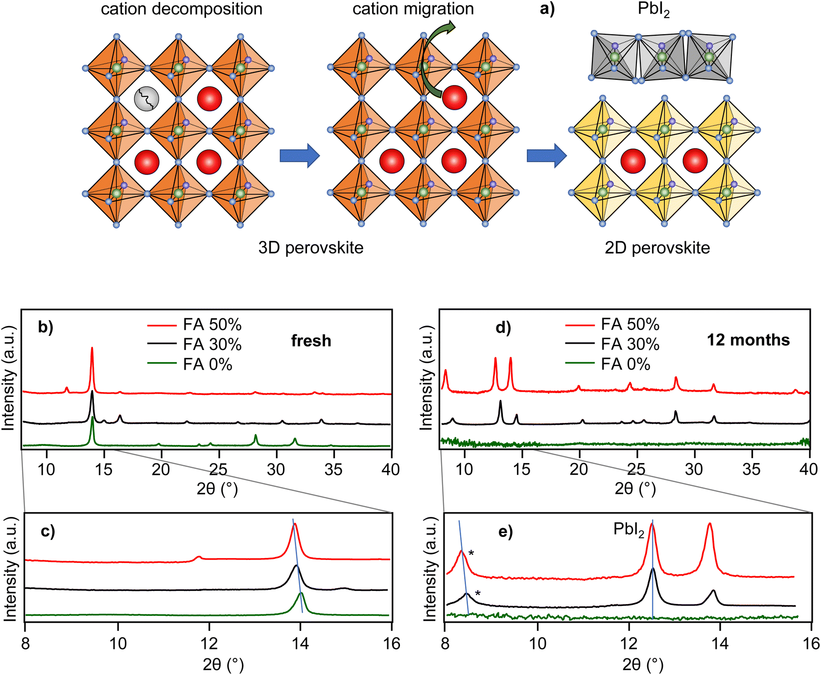 | ||
| Fig. 3 (a) Scheme of the proposed degradation process. X-ray diffraction pattern of freshly prepared (b) and (c), and 12-month-old (d) and (e) perovskite films with compositions as indicated in the legend. The starred peaks in (e) are proposed to correspond to the signal of 2D perovskites. | ||
Further support for the existence of 2D perovskites in the partially degraded films comes from the results of XRD experiments shown in Fig. 3b–e. Freshly prepared films of all three compositions (Fig. 3b and c) show a typical 2θ diffraction peak, which shifts from 14.0° to 13.9° with increasing FA content, as expected for this type of perovskite film.40 After 12 months the diffraction peaks in the FA 0% sample essentially disappear due to progressive degradation. For the FA 30% and FA 50% samples, on the other hand, the perovskite peak at around 14.0° is accompanied by additional peaks at lower angles. The 2θ peaks at 12.7° represent the (001) reflection of PbI2.12 We note that we have not detected any PL signal from PbI2, probably due to its very low PLQY at room temperature. The 2θ peaks at 8.3° (FA 50%) and 8.4° (FA 30%) show a similar shift with the change of composition as the main perovskite peak at around 14.0°, indicating the perovskite origin of these peaks. We note that multiple diffraction peaks at various 2θ angles below the 3D perovskite peak are observed in 2D perovskites with varying number of layers.34 Here, we propose that the observation of the low angle diffraction peaks at 8.3° and 8.4° may support the presence of the 2D perovskite fractions in the partially degraded films.
Degradation of perovskite films in an environment with high humidity has been shown to proceed via hydration intermediates, including monohydrate CH3NH3PbI3·H2O and dihydrate (CH3NH3)4PbI6·2H2O.41,42 Structurally, the monohydrate is a 1D perovskite and we looked into the possibility if this phase could be the origin of the blue-shifted PL. PL spectra of a closely related 1D perovskite crystal have been reported recently.43 The PL bands are indeed blue-shifted from the 3D perovskites but their maxima appear at around 600 nm at room temperature, at far shorter wavelength than the degradation products observed here. Perovskite hydrates are thus unlikely the origin of the blue-shifted emission in the aged perovskite films.
Apart from the above nanoscale spectral characterization, we also analyzed the phenomenon of fluctuations of PL intensity from individual locations in the perovskite films (PL blinking). PL blinking in mixed cation perovskite films has been reported before,15 and it is interesting to verify how film aging affects such nanoscale photophysical properties. An example of PL blinking in the form of PL intensity time trace is shown in Fig. 4a. PL blinking presumably originates from the presence of a very efficient photoactive charge trap in the film which can switch between active and inactive states.19 In the active state, photocarriers which are excited nearby the trap are captured and recombine nonradiatively, leading to a decrease in PL intensity and the appearance of low-intensity bands in the PL blinking trace. If the trap is in its non-active state, such photocarriers recombine radiatively, resulting in high intensities in the PL blinking process. For the blinking analysis we use the concept of potential PL intensity loss, which reflects dynamic PL quenching in the film. This concept is explained in Fig. 4a, which shows an example of widely fluctuating PL intensity over the measurement interval. For further analysis, the intensity is normalized on a scale from 0 to 1. Here, 1 corresponds to the maximum intensity that was recorded from this particular location within the observation interval. This means that this location in the sample is potentially capable of emitting PL with such an intensity (potentially maximum PL) and that PL intensities lower than that indicate PL quenching (PL intensity loss). To quantitatively evaluate this PL quenching, we integrated the blue-shaded area in Fig. 4a. This area corresponds to the total PL intensity loss during the measurement interval. This was further normalized by the total integrated potential intensity (corresponding to the constant potential PL intensity of 1 during the interval) and expressed in percentage points. This value, which we call potential PL intensity loss, reflects the dynamic quenching of PL, that is, the process of activating–deactivating the photoactive charge trap, and it is monitored over a limited time interval of tens of seconds. As such, it does not account for permanent PL quenching or quenching dynamics occurring with much longer time spans. The analysis was carried out for a statistical sample of locations both for the fresh and 12-month-old films.
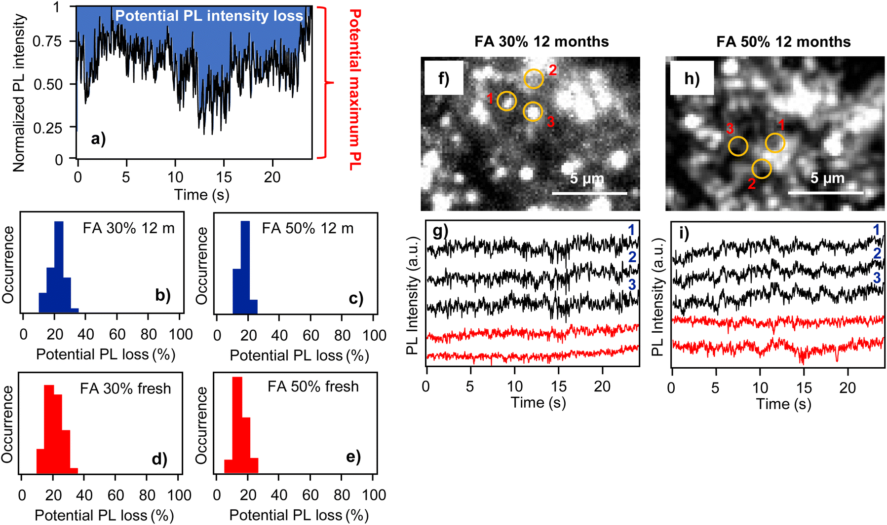 | ||
| Fig. 4 (a) An example of a PL blinking trace indicating schematically the definition of potential PL intensity loss. (b) and (c) Histograms of potential PL intensity loss obtained from PL blinking traces measured 12 months after film preparation, for sample compositions as indicated in the figure. (d) and (e) The same for freshly prepared films. (f) and (h) Microscopic PL images of 12-month-old films. The numbered circles indicate positions where the blinking was analyzed. (g) and (i) PL intensity time traces (blinking) obtained at different locations in the two films, including the positions indicated in (f) and (h). The black traces show highly correlated blinking, the red traces are taken from locations that do not show correlated behavior. | ||
The potential PL intensity loss is presented in the form of a histogram for 12-month-old films of the FA 30% (EA) and FA 50% (EA) samples in Fig. 4b and c. In both samples the peak of distribution has around 20% intensity loss value, with the distribution of the FA 50% (EA) sample being narrower. For comparison, Fig. 4d and e show PL intensity loss distributions for freshly prepared films of the same samples. The peaks of these distributions have around the same 20% loss values, and the distribution of the FA 50% sample is also narrower compared to that of the FA 30% sample. We can thus conclude that film aging does not lead to an increase in the dynamic PL quenching.
Another interesting result comes from the comparison of the blinking traces from different locations in the films. Generally, due to the multi-crystalline nature of the films and the presence of grain boundaries, individual locations in the films are expected to emit PL independently in an uncorrelated manner. Here, comparisons of the PL blinking traces from different locations in the films together with the locations indicated in the PL images are shown in Fig. 4f and g for the FA 30% (EA) sample and in Fig. 4h and i for the FA 50% (EA) sample. In both the samples there are locations (denoted by numbers 1–3) which are separated by several μm, but which show highly correlated PL blinking behavior. In concrete terms, for the FA 30% (EA) film the distances between spots 1 and 2, and those between 1 and 3 are 2.4 μm and 1.8 μm, respectively, and the corresponding Pearson's coefficients calculated for the blinking traces are 0.73 and 0.75. The distances for the 1-to-2 and 1-to-3 locations in the FA 50% (EA) film are 2.1 μm and 2.5 μm, and the Pearson's coefficients are 0.77 and 0.76, respectively. As in the case of the results previously reported on freshly prepared films,15 these values indicate very efficient charge migration over micrometer scales. As mentioned above, the PL blinking originates from the presence of a very efficient photoactive charge trap, which can switch between active and inactive states.19 The fact that we observed well-correlated blinking from locations in the film that are 2–3 μm apart means that these locations share the same charge trap and that the charges are transported to the trap very efficiently over distances of up to ∼3 μm. We note that long-range carrier diffusion in perovskites has been discussed before mainly in terms of delayed PL,44,45 and charge diffusion lengths exceeding 1 μm have been estimated from the lifetime values of trihalide perovskite films.46 In single perovskite microcrystals such charge diffusion estimates are even higher, reaching 4.3 μm in rods and 8.2 μm in platelets.19 Compared to these studies, the spatially correlated blinking in the film observed here provides a direct visualization of efficient charge diffusion.
3. Conclusions
In conclusion, we report long-term ambient air-stable mixed MA/FA cation perovskite films prepared using ethyl acetate as an antisolvent. The films containing 30% and 50% of the FA cation are largely compositionally stable for more than a year as observed from nanoscale PL spectra. In terms of the morphology, the films retain their grain structure but show coalescence into larger crystal grains during the aging process. The morphology change and aging do not affect the long charge diffusion lengths observed for the freshly prepared samples. Slow cation decomposition and migration causes local degradation of the 3D perovskites, presumably into fragments of 2D layered perovskites and PbI2. This process starts from the film edges where the quality of the spin coated film might be lower than in the center. The center area of 5 × 5 mm does not show any signs of compositional degradation in the PL spectra.In contrast, the reference mixed cation samples prepared by an identical process using chlorobenzene as the antisolvent degrade fast within 6 months. Currently, we have not identified any single factor that would solely be responsible for the long term stability of the FA 30% (EA) and FA 50% (EA) films. It is likely a combination of several factors including the optimum tolerance factor in the crystal structure of the two compositions. The main difference between chlorobenzene and ethyl acetate that could affect the long-term stability appears to be the water-absorbing capability of the latter. The use of EA antisolvent ensures that minimum solvent-absorbed water remains in the films even during the fabrication process under ambient conditions with 50% humidity. The lack of residual water in the films then slows down the decomposition of the film from within and assist long-term stability.
4. Experimental section
Synthesis of mixed MA/FA perovskite films
MA1−xFAxPbI3 films with x = 0, 0.3 and 0.5 were synthesized as reported before.15 Prior to the perovskite synthesis, a freshly cleaned microscope cover glass was spin-coated (at 4000 rpm for 40 s) with a 40 nm thick layer of PEDOT:PSS (Clevios P AI4083, H. C. Starck) and annealed at 150 °C for 15 min. To prepare a perovskite film on top of PEDOT:PSS, 1 M perovskite precursor solutions were prepared by mixing PbI2, MAI (methylammonium iodide) and FAI (formamidinium iodide) with molar ratios of 1![[thin space (1/6-em)]](https://www.rsc.org/images/entities/char_2009.gif) :1:0, 1:0.7:0.3 and 1:0.5:0.5, respectively, in a mixed solvent of DMSO (20%) and DMF (80%) by stirring at 60 °C. The precursor solutions were spin-coated on the substrates at 1000 rpm for 10 s followed by 5000 rpm for 30 s. Antisolvents were used in the last 10 s of 5000 rpm spinning by dropping either 100 μL of ethyl acetate (EA) or 100 μL of chlorobenzene (CB). The deposition time of the antisolvent was optimized by choosing different pipette tips and adjusting their diameters. The time range between 0.6 s and ≪0.1 s was tested, and the optimal deposition time of 0.1 s was used in the film preparation process. The films were then annealed at 100 °C for 40 min. The film thickness was around 450 nm, as measured by SEM.
:1:0, 1:0.7:0.3 and 1:0.5:0.5, respectively, in a mixed solvent of DMSO (20%) and DMF (80%) by stirring at 60 °C. The precursor solutions were spin-coated on the substrates at 1000 rpm for 10 s followed by 5000 rpm for 30 s. Antisolvents were used in the last 10 s of 5000 rpm spinning by dropping either 100 μL of ethyl acetate (EA) or 100 μL of chlorobenzene (CB). The deposition time of the antisolvent was optimized by choosing different pipette tips and adjusting their diameters. The time range between 0.6 s and ≪0.1 s was tested, and the optimal deposition time of 0.1 s was used in the film preparation process. The films were then annealed at 100 °C for 40 min. The film thickness was around 450 nm, as measured by SEM.
PL microscopy and spectroscopy
The setup for PL characterization was described previously.15 Briefly, PL from the perovskite films was measured using an inverted microscope (IX 71, Olympus) with 442 nm cw laser excitation. The signal was collected by an oil immersion objective lens (UplanFLN 100×, N.A. 1.3, Olympus) and detected with an electron-multiplying (EM) CCD camera (iXon, Andor Technology) with an exposure time of 30 ms for blinking and of 50 ms for spectral measurements. For spectral measurements the signal was dispersed using an imaging spectrograph (CLP-50LD, Bunkou Keiki) placed between the microscope and the CCD camera.Characterization
Scanning electron microscopy (SEM) was performed using a JSM-7500F (JEOL Ltd). UV–Vis absorption spectra were recorded using a V760 (Jasco) absorption spectrometer. XRD analysis was carried out using a benchtop powder X-ray diffraction instrument (Rigaku MiniFlex 600).Conflicts of interest
There are no conflicts to declare.Acknowledgements
The research was financially supported by the JSPS KAKENHI grants number 19H02684 and number 21K18927, and by the JSPS KAKENHI grant number 23H04875 in a Grant-in-Aid for Transformative Research Areas “Meso-Hierarchical Materials”. AA was financially supported by the Tokyo-Tech pioneering doctoral research program ‘Cross the border!’ scholarship (JST SPRING, Grant Number JPMJSP2106). AA is thankful to Ryotaro Nakamura of Tokyo Institute of Technology for his extensive help with instructions on the use of fluorescence microscopy, data analysis and for stimulating discussions. Akhil Gupta from Deakin university, Australia, Jegadesan Subbiah from Melbourne University, Australia, and Ashish Kulkarni from Forschungszentrum Jülich, Germany, are acknowledged for their helpful discussions and suggestions.References
- H. Min, D. Y. Lee, J. Kim, G. Kim, K. S. Lee, J. Kim, M. J. Paik, Y. K. Kim, K. S. Kim, M. G. Kim, T. J. Shin and I. S. Sang, Nature, 2021, 598, 444–450 CrossRef CAS PubMed
.
- Z. Li, B. Li, X. Wu, S. A. Sheppard, S. Zhang, D. Gao, N. J. Long and Z. Zhu, Science, 2022, 376, 416–420 CrossRef CAS PubMed
- N. J. Jeon, J. H. Noh, Y. C. Kim, W. S. Yang, S. Ryu and S. I. Seok, Nat. Mater., 2014, 13, 897–903 CrossRef CAS PubMed
- A. D. Taylor, Q. Sun, K. P. Goetz, Q. An, T. Schramm, Y. Hofstetter, M. Litterst, F. Paulus and Y. Vaynzof, Nat. Commun., 2021, 12, 1878 CrossRef CAS PubMed
- S. Miao, T. Liu, Y. Du, X. Zhou, J. Gao, Y. Xie, F. Shen, Y. Liu and Y. Cho, Nanomaterials, 2022, 12, 2100 CrossRef CAS PubMed
- J. Troughton, K. Hooper and T. M. Watson, Nano Energy, 2017, 39, 60–68 CrossRef CAS
- Z. Zhang, X. Luo, J. Ding and J. Zhang, J. Solid State Chem., 2019, 274, 199–206 CrossRef CAS
- K. Jung, K. Oh, D. H. Kim, J. W. Choi, K. C. Kim and M. J. Lee, Nano Energy, 2021, 89, 106387 CrossRef CAS
- F. Yang, G. Kapil, P. Zhang, Z. Hu, M. A. Kamarudin, T. Ma and S. Hayase, ACS Appl. Mater. Interfaces, 2018, 10, 16482–16489 CrossRef CAS PubMed
- S. Mazumdar, Y. Zhao and X. Zhang, Stability of Perovskite Solar Cells, Front. Electron., 2021, 2, 712785 CrossRef
- T. Leijtens, K. Bush, R. Cheacharoen, R. Beal, A. Bowring and M. D. McGehee, J. Mater. Chem. A, 2017, 5, 11483–11500 RSC
- B. Charles, J. Dillon, O. J. Weber, M. Saiful Islam and M. T. Weller, J. Mater. Chem. A, 2017, 5, 22495–22499 RSC
- T. Bu, L. Wu, X. Liu, X. Yang, P. Zhou, X. Yu, T. Qin, J. Shi, S. Wang, S. Li, Z. Ku, Y. Peng, F. Huang, Q. Meng, Y. B. Cheng and J. Zhong, Adv. Energy Mater., 2017, 7, 1700576 CrossRef
- K. P. Goetz, A. D. Taylor, F. Paulus and J. Vaynzof, Adv. Funct. Mater., 2020, 30, 1910004 CrossRef CAS
- A. Agarwal, S. Omagari and M. Vacha, ACS Energy Lett., 2022, 7, 2443–2449 CrossRef CAS
- C. Li, Y. Zhong, C. A. Luna, T. Unger, K. Deichsel, A. Gräser, J. Köhler, A. Köhler, R. Hildner and S. Huettner, Molecules, 2016, 21, 1081 CrossRef PubMed
- S. Draguta, S. Thakur, Y. V. Morozov, Y. Wang, J. S. Manser, P. V. Kamat and M. Kuno, J. Phys.
Chem. Lett., 2016, 7, 715–721 CrossRef CAS PubMed
- M. Chauhan, Y. Zhong, K. Schötz, B. Tripathi, A. Köhler, S. Huettnerc and F. Panzer, J. Mater. Chem. A, 2020, 8, 5086–5094 RSC
- H. Yuan, E. Debroye, E. Bladt, G. Lu, M. Keshavarz, K. P. Janssen, M. B. Roeffaers, S. Bals, E. H. Sargent and J. Hofkens, Adv. Mater., 2018, 30, 1705494 CrossRef PubMed
- A. Merdasa, M. Bag, Y. Tian, E. Källman, A. Dobrovolsky and I. G. Scheblykin, J. Phys. Chem. C, 2016, 120, 10711–10719 CrossRef CAS
- S. Kundu and T. L. Kelly, EcoMat, 2020, 2, e12025 CrossRef CAS
- E. Smecca, V. Valenzano, I. Deretzis, S. Valastro, S. Carallo, S. Colella, G. Mannino, A. Rizzo, A. La Magna and A. Alberti, J. Phys. Chem. C, 2022, 126, 16825–16833 CrossRef CAS
- E. J. Juarez-Perez, L. K. Ono, M. Maeda, Y. Jiang, Z. Hawash and Y. Qi, J. Mater. Chem. A, 2018, 6, 9604–9612 RSC
- G. Abdelmageed, L. Jewell, K. Hellier, L. Seymour, B. Luo, F. Bridges, J. Z. Zhang and S. Carter, Appl. Phys. Lett., 2016, 109, 233905 CrossRef
- S. Chen, X. Zhang, J. Zhao, Y. Zhang, G. Kong, Q. Li, N. Li, Y. Yu, N. Xu, J. Zhang, K. Liu, Q. Zhao, J. Cao, J. Feng, X. Li, J. Qi, D. Yu, J. Li and P. Gao, Nat. Commun., 2018, 9, 4807 CrossRef PubMed
- Z. Song, A. Abate, S. C. Watthage, G. K. Liyanage, A. B. Phillips, U. Steiner, M. Graetzel and M. J. Heben, Adv. Energy Mater., 2016, 6, 1600846 CrossRef
- J. Yang, B. D. Siempelkamp, D. Liu and T. L. Kelly, ACS Nano, 2015, 9, 1955–1963 CrossRef CAS PubMed
- K. Jemli, H. Diab, F. Lédée, G. Trippé-Allard, D. Garrot, B. Geffroy, J.-B. Lauret, P. Audebert and E. Deleporte, Molecules, 2016, 21, 885 CrossRef PubMed
- J. Li, A. Dobrovolsky, A. Merdasa, E. L. Unger and I. G. Scheblykin, ACS Omega, 2018, 3, 14494–14502 CrossRef CAS PubMed
- M. Chauhan, Y. Zhong, K. Schötz, B. Tripathi, A. Köhler, S. Huettnerc and F. Panzer, J. Mater. Chem. A, 2020, 8, 5086–5094 RSC
- F. Zhang, S. Huang, P. Wang, X. Chen, S. Zhao, Y. Dong and H. Zhong, Chem. Mater., 2017, 29, 3793–3799 CrossRef CAS
- A. Merdasa, A. Kiligaridis, C. Rehermann, M. Abdi-Jalebi, J. Stöber, B. Louis, M. Gerhard, S. D. Stranks, E. L. Unger and I. G. Scheblykin, ACS Energy Lett., 2019, 4, 1370–1378 CrossRef CAS
- X. Li, J. M. Hoffman and M. C. Kanatzidis, Chem. Rev., 2021, 121, 2230–2291 CrossRef CAS PubMed
- S. Ghimire and C. Klinke, Nanoscale, 2021, 13, 12394 RSC
- C. M. M. Soe, G. P. Nagabhushana, R. Shivaramaiah, H. Tsai, W. Nie, J.-C. Blancon, F. Melkonyan, D. H. Cao, B. Traoré, L. Pedesseau, M. Kepenekian, C. Katan, J. Even, T. J. Marks, A. Navrotsky, A. D. Mohite, C. C. Stoumpos and M. G. Kanatzidis, Proc. Natl. Acad. Sci. U. S. A., 2019, 116, 58–66 CrossRef PubMed
- J. Liu, J. Leng, K. Wu, J. Zhang and S. Jin, J. Am. Chem. Soc., 2017, 139, 1432–1435 CrossRef CAS PubMed
- W. Wang, M. Cai, Y. Wu, K. Ji, B. Cheng, X. Liu, H. Lv and S. Dai, Symmetry, 2022, 14, 1099 CrossRef CAS
- A. Merdasa, M. Bag, Y. Tian, E. Källman, A. Dobrovolsky and I. G. Scheblykin, J. Phys. Chem. C, 2016, 120, 10711–10719 CrossRef CAS
- J.-C. Blancon, H. Tsai, W. Nie, C. C. Stoumpos, L. Pedesseau, C. Katan, M. Kepenekian, C. M. M. Soe, K. Appavoo, M. Y. Sfeir, S. Tretiak, P. M. Ajayan, M. G. Kanatzidis, J. Even, J. J. Crochet and A. D. Mohite, Science, 2017, 355, 1288–1292 CrossRef CAS PubMed
- Y. Zhang, G. Grancini, Y. Feng, A. M. Asiri and M. K. Nazeeruddin, ACS Energy Lett., 2017, 2, 802–806 CrossRef CAS
- A. M. A. Leguy, Y. Hu, M. Campoy-Quiles, M. I. Alonso, O. J. Weber, P. Azarhoosh, M. van Schilfgaarde, M. T. Weller, T. Bein, J. Nelson, P. Docampo and P. R. F. Barnes, Chem. Mater., 2015, 27, 3397–3407 CrossRef CAS
- J. Yang, B. D. Siempelkamp, D. Liu and T. L. Kelly, ACS Nano, 2015, 9, 1955–1963 CrossRef CAS PubMed
- X. Cheng, J. Ma, X. Zhou, C. Fang, J. Wang, J. Li, X. Wen and D. Li, JPhys Photonics, 2020, 2, 014008 CrossRef CAS
- S. Ghimire, L. Chouhan, Y. Takano, K. Takahashi, T. Nakamura, K. Yuyama and V. Biju, ACS Energy Lett., 2019, 4, 133–141 CrossRef CAS
- Z. Zhang, S. Ghimire, T. Okamoto, B. M. Sachith, J. Sobhanan, C. Subrahmanyam and V. Biju, ACS Nano, 2022, 16, 160–168 CrossRef CAS PubMed
- S. D. Stranks, G. E. Eperon, G. Grancini, C. Menelaou, M. J. P. Alcocer, T. Leijtens, L. M. Herz, A. Petrozza and H. J. Snaith, Science, 2013, 342, 341–344 CrossRef CAS PubMed
Footnote |
| † Electronic supplementary information (ESI) available. See DOI: https://doi.org/10.1039/d3nr02003g |
| This journal is © The Royal Society of Chemistry 2023 |