
 Open Access Article
 This Open Access Article is licensed under a
 Creative Commons Attribution 3.0 Unported Licence
Self-limiting stoichiometry in SnSe thin films†
Jonathan R. Chin a,
Marshall B. Fryea,
Derrick Shao-Heng Liub,
Maria Hilsec,
Ian C. Grahama,
Jeffrey Shallenbergerc,
Ke Wangc,
Roman Engel-Herbertd,
Mengyi Wangb,
Yun Kyung Shine,
Nadire Nayiref,
Adri C. T. van Duine and
Lauren M. Garten
*a
a,
Marshall B. Fryea,
Derrick Shao-Heng Liub,
Maria Hilsec,
Ian C. Grahama,
Jeffrey Shallenbergerc,
Ke Wangc,
Roman Engel-Herbertd,
Mengyi Wangb,
Yun Kyung Shine,
Nadire Nayiref,
Adri C. T. van Duine and
Lauren M. Garten
*a
aThe School of Materials Science and Engineering, Georgia Institute of Technology, Atlanta, Georgia 30332-0245, USA. E-mail: lauren.garten@mse.gatech.edu
bDepartment of Materials Science and Engineering, The Pennsylvania State University, University Park, Pennsylvania 16802, USA
cMaterials Research Institute, The Pennsylvania State University, University Park, Pennsylvania 16802, USA
dPaul-Drude Institut für Festkörperelektronik Berlin, Leibniz-Institut im Forschungsverbund Berlin eV., Berlin 10117, Germany
eDepartment of Mechanical Engineering, The Pennsylvania State University, University Park, Pennsylvania 16802, USA
fPhysics Department, Karamanoglu Mehmetbey University, Karaman, 70000, Turkey
First published on 5th June 2023
Abstract
Unique functionalities can arise when 2D materials are scaled down near the monolayer limit. However, in 2D materials with strong van der Waals bonds between layers, such as SnSe, maintaining stoichiometry while limiting vertical growth is difficult. Here, we describe how self-limiting stoichiometry can promote the growth of SnSe thin films deposited by molecular beam epitaxy. The Pnma phase of SnSe was stabilized over a broad range of Sn![[thin space (1/6-em)]](https://www.rsc.org/images/entities/char_2009.gif) :Se flux ratios from 1:1 to 1:5. Changing the flux ratio does not affect the film stoichiometry, but influences the predominant crystallographic orientation. ReaxFF molecular dynamics (MD) simulation demonstrates that, while a mixture of Sn/Se stoichiometries forms initially, SnSe stabilizes as the cluster size evolves. The MD results further show that the excess selenium coalesces into Se clusters that weakly interact with the surface of the SnSe particles, leading to the limited stoichiometric change. Raman spectroscopy corroborates this model showing the initial formation of SnSe2 transitioning into SnSe as experimental film growth progresses. Transmission electron microscopy measurements taken on films deposited with growth rates above 0.25 Å s−1 show a thin layer of SnSe2 that disrupts the crystallographic orientation of the SnSe films. Therefore, using the conditions for self-limiting SnSe growth while avoiding the formation of SnSe2 was found to increase the lateral scale of the SnSe layers. Overall, self-limiting stoichiometry provides a promising avenue for maintaining growth of large lateral-scale SnSe for device fabrication.
:Se flux ratios from 1:1 to 1:5. Changing the flux ratio does not affect the film stoichiometry, but influences the predominant crystallographic orientation. ReaxFF molecular dynamics (MD) simulation demonstrates that, while a mixture of Sn/Se stoichiometries forms initially, SnSe stabilizes as the cluster size evolves. The MD results further show that the excess selenium coalesces into Se clusters that weakly interact with the surface of the SnSe particles, leading to the limited stoichiometric change. Raman spectroscopy corroborates this model showing the initial formation of SnSe2 transitioning into SnSe as experimental film growth progresses. Transmission electron microscopy measurements taken on films deposited with growth rates above 0.25 Å s−1 show a thin layer of SnSe2 that disrupts the crystallographic orientation of the SnSe films. Therefore, using the conditions for self-limiting SnSe growth while avoiding the formation of SnSe2 was found to increase the lateral scale of the SnSe layers. Overall, self-limiting stoichiometry provides a promising avenue for maintaining growth of large lateral-scale SnSe for device fabrication.
 Lauren M. Garten | Lauren Garten is an assistant professor in the School of Materials Science and Engineering at the Georgia Institute of Technology. Her research is on the development of multiferroic materials for energy and electronic applications. Her particular focus lies at the nexus between ferroelectricity, magnetism, and photovoltaics. Prior to coming to Georgia Tech, Dr Garten was a scientist at the U.S. Naval Research Lab, and a post-doc at the National Renewable Energy Laboratory. She has won the ONR Young Investigator Award, AFOSR Young Investigator Award, the Intel Rising Star Award, the DOE-BES Postdoctoral Research Award, and the CalTech Young Investigator Lectureship. |
Introduction
Controlling layered growth in 2D materials is critical for the emergence of unique properties.1 However, creating a stoichiometric monolayer thick film with lateral dimensions sufficient for device fabrication is challenging even in materials with van der Waals (vdW) bonding between layers. Mechanical exfoliation of layers from a single crystal is effective for materials such as MoS2 and graphene which have weak inter-layer (vdW) bonds along the out-of-plane direction.2–4 But as the interlayer bond strength increases, mechanical exfoliation becomes increasingly difficult, necessitating a different monolayer isolation approach. For example, tin selenide (SnSe) is a vdW material that will exhibit unique functionalities if it can be scaled down near the monolayer limit. When reduced to a single layer, SnSe transitions from the centrosymmetric space group Pnma to the non-centrosymmetric Pmn21.5,6 The reduced symmetry manifests several unique properties, including piezoelectricity, pyroelectricity, and second harmonic generation.5,7–10 Monolayer SnSe is predicted to possess a d11 piezoelectric coefficient of 74.73 pm V−1; an order of magnitude greater than currently established two dimensional (2D) materials like MoS2 (d11 = 3.7 pm V−1).11 Piezoelectric measurements on 35 nm thick SnSe films have shown a d11 coefficient of 19.9 pm V−1 despite not having a compatible symmetry for piezoelectricity.12 Achieving the full piezoelectric response will require scaling down to an odd number of layers near the monolayer limit.In addition to the emergence of new properties, dimensional scaling can also be used for property tuning in vdW materials. Decreasing the number of layers has been shown to change the band gap from 0.9 eV in bulk13 to 1.4 eV at the monolayer limit, making SnSe an interesting platform to study the impact of thickness scaling on the photovoltaic response.14 Additionally, SnSe is most well-known for its ideal thermoelectric properties, which increases responsivity as the thickness scales down.15 Therefore, developing layer control will be a critical factor in maximising the application of SnSe.
However, unlike common 2D piezoelectric films like MoS2 and graphene, SnSe possesses relatively strong interlayer forces, rendering it difficult to isolate a monolayer.5,7,9,16 Density functional theory (DFT) calculations indicate interlayer binding energies reach 146 meV per atom in SnSe compared to only 24 meV per atom for graphite.17 The lone pair electrons on Sn are thought to contribute to the enhanced interlayer bonding.18 Additionally the mixed Sn and Se layer termination (unlike materials such as SnSe2 in which there is only Se in the surface layer) likely further contributes to the increase in interlayer bond strength. Therefore, in SnSe and other materials with Rydberg ions or complex layer termination, mechanical exfoliation will be less effective for the isolation of independent layers, necessitating a different approach for the controlled selection of layers.
Rather than extracting a single layer (6.8 Å) from a bulk crystal, direct deposition methods such as a chemical vapor deposition (CVD), physical vapor deposition (PVD), and molecular beam epitaxy (MBE) present viable alternatives for creating monolayer SnSe.7,19–23 CVD has been used to synthesize monolayer SnSe with lateral dimensions up to 50 μm by post etching after CVD growth,24 but etching can induce damage in the material and affect device properties. MBE has also stabilized SnSe thin films down to a single atomic monolayer, but with limited lateral scaling below 200 nm.6,25
Maintaining stoichiometry within a single layer is a difficult prospect for MBE growth. One solution is varying the shutter timing of individual effusion cells. This approach has been used to stabilize metastable materials such as Ruddlesden–Poppers ((SrTiO3)50SrO),26 and hexagonal ferrites (ScFeO3),27 where each layer is compositionally discrete. However, shutter variation cannot be applied to SnSe because the layer termination has mixed composition.
Beyond changing the timing, the adatom mobility is also critical in order to provide sufficient mobility for the incoming atoms to make it to the edge of a preexisting nanoplate.28,29 But balancing layer growth while maintaining a fixed stoichiometry is further complicated in SnSe because of the narrow temperature window for the formation of the desired Pnma phase. The phase formation temperature is significantly higher than the temperature of the selenium effusion cell. There is a high volatility of selenium and a low sticking coefficient, leading to constant reentrant growth.30
Supplying an excess of a volatile component has been shown to be useful in maintaining stoichiometry in some lead and bismuth containing compounds, but this method works best when there is a mechanism of self-limiting stoichiometry. For example, it has been shown in Bi4Ti3O12 and Bi2Sr2CuO6 thin films deposited by MBE that a surplus of bismuth doesn't affect composition due to the low sticking coefficient of bismuth and the evaporation of the different phases at deposition temperatures.31 Therefore, a deeper understanding of the tin and selenium interactions and kinetics is needed in order to find the balance needed to control layer scaling while still maintaining stoichiometry.
This work investigates the stabilization of SnSe during MBE growth. The impact of flux ratio and temperature on the formation of SnSe are studied using the combination of experimental measurements and ReaxFF MD simulations. SnSe films are grown by molecular beam epitaxy over a broad range of flux ratios from 1:1 to 1:5. A series of ReaxFF molecular dynamics simulations are performed using a newly developed ReaxFF Sn/Se parameter set to characterize the initial stages of phase formation and study the effects of these flux ratios on initial Sn/Se cluster formation. The progressive phase formation leading to stabilization of 1:1 SnSe over time is further corroborated by the experimental characterization of the structure and composition of SnSe films captured at different stages of growth. These results provide a deeper understanding of the tin and selenium interactions and kinetics that lead to self-limiting stoichiometries in SnSe.
Experimental methods
Film growth
Thin films of SnSe were deposited by MBE. The films were deposited onto either as purchased, furnace annealed, or cleaved (100) MgO, and (0001) Al2O3 from MTI Corp. All substrates were cleaned by subsequent ultrasonication in acetone, isopropyl alcohol, and DI water before loading them into the ultra-high vacuum (UHV) environment. Furnace annealed MgO substrates were subject to a thermal treatment to at 1000 °C for 40 to 80 min in a tube furnace flowing 80 sccm of oxygen per minute and a subsequent secondary solvent cleaning procedure before their use in MBE. Upon loading substrates into the UHV environment, the remaining water film on all substrates resulting from their preparation in air was removed by a heating cycle to 120 °C for 1 h in UHV. MgO substrates were then transferred into the growth chamber and annealed a second time in UHV at 900 °C for 10 minutes prior to growth, unless otherwise specified.MgO was selected because of the potential to promote the out of plane orientation of SnSe due to the comparable lattice matching between the cubic MgO substrate with the lattice constant a = 4.29 Å and the b–c plane of the orthorhombic SnSe (a = 11.490 Å, b = 4.440 Å, c = 4.135 Å).32,33 The background pressure of the MBE was maintained at or below 2.5 × 10⁻⁹ Torr throughout the UHV annealing setup and during thin film deposition.
A quartz crystal monitor independently measured the flux rate for each effusion cell prior to deposition. The tin to selenium flux ratios ranged from 1:1 to 1:5 (Sn:Se). The substrate temperature was kept constant for each run. Substrate temperatures over a range from 200–350 °C were tested. In situ reflection high energy electron diffraction (RHEED) measurements were taken using a 15 kV Staib Instruments electron gun with the kSA 400 RHEED software. Individual trials lasted for time periods ranging from 22 s to 5 h, after which each sample was allowed to cool prior to removal from vacuum.
Film characterization
The structure of the films, including phase and crystallographic orientation, was characterized using a Panalytical X'Pert3 4-circle X-ray diffraction (XRD) system in high resolution with a PIXcel 3D detector and Cu Kα1 source. Thin film crystal structure was also characterized by a 200 kV FEI dual aberration corrected scanning/transmission electron microscope (S/TEM) in high-angle annular dark field (HAADF) imaging and with plane-view Raman spectroscopy on a Horiba LabRam system using 532 nm laser excitation and a neutral power density filter of 1% while the laser was focused through a 100× objective in backscattering geometry, and the spectral resolution set by the grating of 1800 g mm−1. Atomic force microscopy (AFM) measurements of the thin film morphology were performed with a Dimension Icon Bruker AFM operated in Peak-Force Tapping mode. The probe tips used were the SCANASYST-AIR silicon on nitride and the RTESPA-150 antimony doped silicon.The composition of the films was assessed by X-ray photoelectron spectroscopy (XPS) using a Physical Electronics VersaProbe II and a Thermo K-Alpha XPS, both with Al Kα sources (1486.6 eV). An IONTOF time-of-flight secondary ion mass spectrometer (ToF-SIMS) with a Bi nanoprobe ion source corroborated the relative quantities of Sn and Se.
Theoretical calculations
ReaxFF method
The ReaxFF reactive force field34 has been developed to model chemically dynamical systems, offering accuracy approaching that of quantum mechanics (QM) based methods at a significantly low computational cost. ReaxFF employs a bond-order formalism with polarizable charge description, where the bond order is empirically calculated based on interatomic distances. The total potential energy of a system is summed over the following contributions:
 | (1) |
Force field parameterization
The Sn/Se quantum mechanics (QM) data set for the force field parameterization includes the heats of formation and equations of state of bulk alpha-Sn, orthorhombic (Pnma) SnSe, cubic (Fm![[3 with combining macron]](https://www.rsc.org/images/entities/char_0033_0304.gif) m) SnSe and trigonal (Pm1) SnSe2, as well as the binding energies of various SnxSey clusters with different Sn:Se ratios. The following ReaxFF parameters were optimized against the QM data: the Sn atom parameters, Sn–Sn and Sn–Se-related bond, off-diagonal, and angle parameters. During parameterization, a single-parameter search algorithm was used to minimize the error between ReaxFF and reference values.36 The condensed and gas phases feature a reasonable agreement between the trained force field and DFT, as seen in Fig. S1,† a free energy plot as a function of composition. This shows the heats of formation and equations of state for SnSen crystals where n = 0, 1, 2.
m) SnSe and trigonal (Pm1) SnSe2, as well as the binding energies of various SnxSey clusters with different Sn:Se ratios. The following ReaxFF parameters were optimized against the QM data: the Sn atom parameters, Sn–Sn and Sn–Se-related bond, off-diagonal, and angle parameters. During parameterization, a single-parameter search algorithm was used to minimize the error between ReaxFF and reference values.36 The condensed and gas phases feature a reasonable agreement between the trained force field and DFT, as seen in Fig. S1,† a free energy plot as a function of composition. This shows the heats of formation and equations of state for SnSen crystals where n = 0, 1, 2.
Molecular dynamics simulations
To resemble experimental flux ratios in the presence of excess Se, the ReaxFF calculations used a Sn:Se ratio of 1:4. To understand what is occurring during the initial stages of growth, the system was constructed by randomly placing 25 Sn4 and 200 Se2 molecules in an 80 Å × 80 Å × 80 Å simulation box with periodic boundary conditions. After energy minimization, molecular dynamics (MD) equilibration was performed with a 0.25 fs time step for 1.25 ns at 500 K in the canonical (NVT) ensemble. The temperature was controlled by the Berendsen thermostat with a damping constant of 100 fs.
To examine further the dependence of Se diffusivity on the local chemical environment, we determined the diffusion coefficients of Se in a liquid Se92 cluster and in a Se cluster (Se92 and Se292) bound on Sn100Se70-cluster surface; all configurations were taken from the trajectories of Sn/Se growth simulation. The liquid cluster was inserted into the center of a simulation box of 79.85 Å × 79.73 Å × 79.25 Å. The systems were equilibrated at 500 K for up to 200 ps in an NVT ensemble with a temperature damping constant of 100 fs. To collect trajectories for the calculation of the diffusion coefficient, the NVT MD simulations were performed for 1.5–2 ns, using a weak thermostat coupling of 1000 fs.
Results & discussion
The first step toward SnSe film growth is identifying the processing window for 1:1 SnSe in the bulk Pnma phase. Given the volatility of selenium,30 the initial focus is on determining the ratio of Sn:Se flux that creates stoichiometric films. Nominal flux ratios of Sn:Se from 1:1 to 1:5 were used to determine the range over which SnSe could be achieved at a fixed growth temperature of 280 ± 5 °C. Fig. 1 shows the X-ray diffraction results for films grown on cleaved MgO under different flux ratios. Observed diffraction peaks at 15°, 31°, 47°, and 65° were attributed to the (200), (400), (600), and (800) planes of the desired Pnma phase of SnSe37,38 labeled by ◆ in Fig. 1.39 The MgO peak is denoted by * at 43°.40 SnSe forms over the entire range of investigated nominal flux ratios. Although bulk SnSe is known to be a line compound,41 such behavior is well known for self-assembled, self-limited growth methods at non-equilibrium conditions like MBE, where over-supplied atoms or molecules simply desorb from the growth front once a certain energetically favorable configuration in the film or nucleus is reached. However, at low Se supply, i.e., nominal flux ratios of 1:3 and lower, additional diffraction peaks emerge systematically attributed to the elemental Sn42 formation in the tetragonal beta phase. Thus, at these flux ratios, the supplied Se flux was not able to saturate all supplied Sn atoms to form the SnSe phase and excess Sn formed in these samples. On the other hand, at too large of Se oversupply, i.e., flux ratio of 1:5, out-of-plane orientations of SnSe emerge in the XRD data in Fig. 1 as diffraction peaks at 25.4° and 37.9° corresponding to the {201} and {311} plane family of SnSe, respectively. There are also three low-intensity peaks on either side of the (200) peak at 13.8°, 16.6°, and 18.2°, which could potentially be thickness fringes from the SnSe thin film. Their spacing indicates a thickness of 6 nm. However, the SnSe film thickness was nominally estimated to be 49.8 nm, which correlates with the thickness value of 55 nm extracted from the XRD data shown in Fig. 1 using the Scherrer43 equation but is in discrepancy with the 6 nm found for the thickness fringes. It is thus more likely that the thickness fringes arise from a parasitic SnSe2 layer in the film. Indeed, literature attributes the {001} hexagonal SnSe2 orientations to both the peaks at 13.8°44 and 16.6°,45 labeled with the symbols  and ✦, respectively. The appearance of parasitic SnSe2 fingerprints in the XRD data point toward a relatively uncontrolled formation process that does not depend on the supplied Sn:Se flux ratio. SnSe2 might form under conditions that are not well controlled like a certain local substrate termination or defect. This secondary phase might also form during cool-down of the sample after SnSe growth while still in the Se atmosphere remaining in the chamber even after the shutter was closed due to its high volatility and the required oversupply. Assuming all three peaks at 13.8°, 16.6°, and 18.2° relate to SnSe2, the thickness values found from the thickness fringes (6 nm) match much better with the Scherrer equation value for either one of the SnSe2 attributed peaks (11 nm and 13 nm, respectively). Besides revealing a trace amount of SnSe2 present in some of the samples, this study determined the optimal flux ratio for solely SnSe phase formation to be nominally 1:4, which translated to a 1:1 Sn:Se stoichiometry in the film as confirmed by XPS measurements (Fig. 2a).
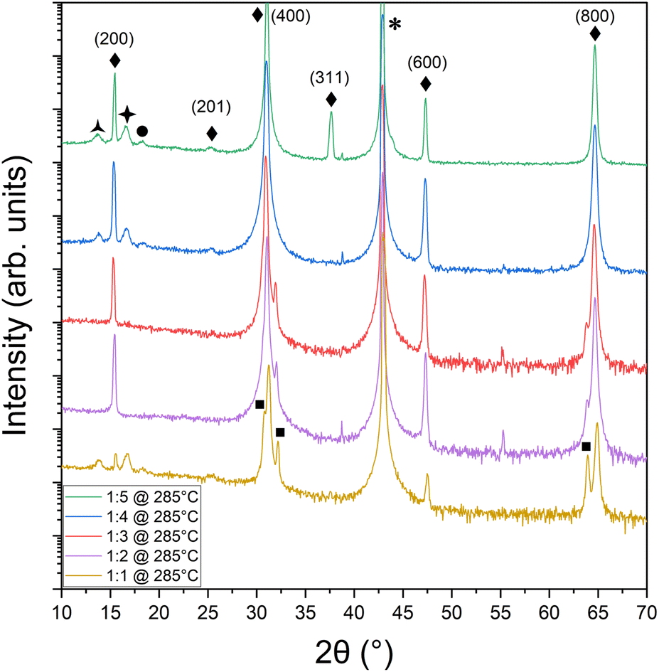 | ||
Fig. 1 XRD of SnSe thin films grown on MgO for 83 minutes at 280 ± 5 °C for five Sn:Se flux ratios ranging from 1:1 to 1:5 showing the formation of SnSe for all flux ratios. The ◆ is Pnma SnSe (PDF 04-009-2257/01-088-2862), the  is Pm1 SnSe2 (PDF 01-089-2939); the ✦ could be attributed to a thickness fringe or Pm1 SnSe2 (PDF 01-086-8651), the ● would correspond to the next order thickness fringe from ✦; * is MgO (PDF 00-004-0829), and the ■ is I41/amd Sn (PDF 04-004-7747). is Pm1 SnSe2 (PDF 01-089-2939); the ✦ could be attributed to a thickness fringe or Pm1 SnSe2 (PDF 01-086-8651), the ● would correspond to the next order thickness fringe from ✦; * is MgO (PDF 00-004-0829), and the ■ is I41/amd Sn (PDF 04-004-7747). | ||
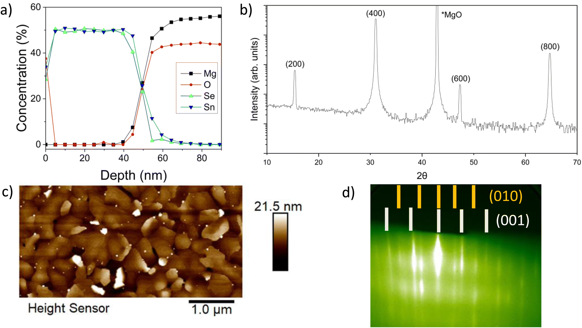 | ||
| Fig. 2 (a) XPS depth profile of a SnSe thin film deposited on MgO with 1:4 Sn:Se flux ratio at 280 ± 5 °C for 83 minutes. (b) XRD of the film in 2a indicating (200) orientation out-of-plane, (c) AFM on the same film showing mixed orientation distribution in-plane, and (d) RHEED measurements of a SnSe film with multiple in-plane orientations taken post growth. | ||
Fig. S2† shows SnSe samples grown on Al2O3 that show a similar trend, but with the (210) and (420) orientations appearing first with the substrate peak at the 1:1 flux ratio. Then as the flux ratio increases the {200} family of planes emerges, becoming more prevalent over the {210} family of planes at the 1:4 flux ratio.
Previous reports have also shown that SnSe could be stabilized over a range of fluxes (1:0.8–1:7), but that a 1:1 flux ratio results in highest crystalline quality Pnma SnSe on (100) MgO.32 Other reports show that a flux ratio of 1:1 stabilizes SnSe but in the metastable rock-salt phase (a = 4.23 Å) on Bi2Se3.46 Still other reports show that flux ratio of Sn:Se of 1:3 and above (up to 40) yield SnSe2 films on GaAs (111) substrates.47 But we find that over a temperature range of 250–285 °C there is no temperature dependent change in the SnSe concentration by XRD, shown in Fig. S3† for a single flux ratio of 1:4. Increasing temperature up to 275–285 °C led to a predominant orientation along the basal plane of SnSe. Above 300 °C no films were observed by XRD, indicating the volatilization of SnSe from the substrate. Given that increasing the lateral scaling of SnSe monolayers requires promoting a single crystal orientation along the basal plane, 280 ± 5 °C was chosen for subsequent growths.
To understand how the stoichiometry evolves during growth, XPS depth profiles were taken over the thickness of SnSe films. Fig. 2a shows the results of an XPS depth profile for a film grown with a flux rate of 1:4 at 280 ± 5 °C. Under these conditions, a deposition time of 83 minutes resulted in an approximately 0 nm thick film – indicating a growth rate of 0.6 nm min−1. The equivalent quantities of Sn and Se throughout the thickness of the films indicate that the films are stoichiometrically SnSe. From the surface to a depth of approximately 5 nm there is a decrease in the oxygen concentration, indicating that a surface oxide, such as SnO2, is present but limited to the near surface region of the film. There is also potential diffusion at the film-substrate interface. There are no other indications of secondary phases with differing tin to selenium stoichiometries in the thick films.
A 1:4 ratio produces the best out-of-plane orientation, as deduced from our earlier XRD study in Fig. 1 and confirmed reproducibly by the XRD analysis in Fig. 2b for another sample. Key SnSe XRD peaks are attributed to (2h00)-oriented single phase Pnma SnSe.37,38 Besides the MgO substrate peak, no other orientations or phases are observed. These results demonstrate that the out-of-plane orientation is along the basal plane of SnSe, which is in agreement with the 2D layered structure of SnSe.
While the XRD data suggests that the films are well aligned, the AFM results provide a more detailed picture. From the AFM data in Fig. 2c (taken on the same sample as Fig. 2a and b), there is a clear surface roughness and morphology texture apparent in the film. Between regions with smooth surfaces of layered terrace growth are some additional misaligned, i.e., taller out-of-plane oriented domains with irregularly shaped morphologies interspersed throughout. The AFM results are further corroborated by in situ RHEED shown in Fig. 2d, depicting clear streaks consistent with Pnma SnSe with a pronounced high-angle rotational domain formation resulting in an isotropic RHEED pattern displaying both orientations [(010) and (001)] simultaneously. This clearly delineated patterning indicates a relatively smooth film growth, despite the presence of high-angle rotational domains.48 The formation of high-angle rotational domains will limit the lateral scales of in-plane growth. Therefore, the next step is to further investigate how stoichiometry and structure develop during the initial stages of growth to understand the mechanisms at play as the film is crystallizing.
To understand what is occurring during the initial stages of growth, a ReaxFF model was developed to track the interactions between tin and selenium during evaporation and deposition. The formation of SnxSey clusters is tracked as a function of time under conditions that emulate those in the deposition chamber. Fig. 3a illustrates the evolution of the heaviest SnSe cluster. In the first 1.8 ps of simulation, two Se dimers approached and bonded to an Sn4 molecule, creating an Sn4Se4 cluster. The small clusters gradually join each other as the formation of Sn–Se bonds is energetically more favorable. As shown in Fig. 3b, the Sn:Se ratios of the 10 heaviest clusters indicate the formation of both SnxSex and SnxSe2x clusters at the beginning of the simulation until around 600 ps. As cluster size evolves, we observe that although the surface becomes Sn-rich, the core of the cluster features the Sn:Se ratio of 1:1 (Fig. S4†). This indicates that as we approach bulk structure and – by consequence – the ratio of surface/core shrinks, our stoichiometric ratio will be transitioning to a 1:1 ratio. These results are further corroborated by experimental ToF-SIMS analysis that indicates a decrease in the Sn:Se ratio from 1.78 at the surface to 0.85 for a film deposited with a 1:2 flux ratio at 280 ± 5 °C on an MgO substrate. As seen in Fig. S5,† the reduced ratio of Sn:Se normalizes after a certain depth, which supports the self-limiting nature of SnSe. Our computed powder diffraction analysis in Fig. S6† provides additional support to the observed 1:1 ratio, showing that the majority of the primary peaks from our SnSe cluster match with a face-centered structure (indexed with Fmm) while the rest of the peaks match with an orthorhombic structure (indexed with Pnma). Starting from t = 492.5 ps to the end of the simulation, the excessive Se content coalesces, forms aggregated Se clusters, and is bound to the surface of the SnSe cluster. Another result drawn from our simulations is that the structure of the SnSe cluster is relatively insensitive to the molecule sizes of Sn and Se precursors (Fig. S4†). Additionally, in accordance with experimental observations under flux ratios from 1:1 to 1:4, the presence of excessive Se does not alter the stoichiometry of the SnSe cluster. These simulation results confirm the stability of SnSe stoichiometry under a broad window of flux ratio.
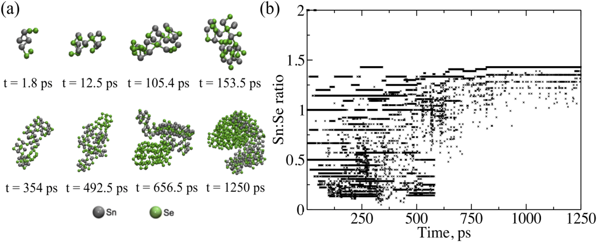 | ||
| Fig. 3 (a) Snapshots of the heaviest SnxSey cluster during growth. (b) Stoichiometric ratios of the 10 heaviest SnxSey clusters in the system at each time interval. | ||
To further understand the growth mechanism of SnSe, the atomic diffusion of Se in a liquid Se292 cluster on Sn100Se70-cluster (Fig. 4) was evaluated by performing MD simulations at 500 K. This temperature was selected to match the experimental conditions. Fig. 4a displays the time-dependent mean-square displacement (MSD) of Se atoms in the Se cluster. The diffusion coefficient, determined from a least-square fit to the MSD by the Einstein formula,49 is 0.42 × 10⁻¹⁰ m2 s−1, which is quantitatively close to that of a free Se liquid cluster obtained from the MD simulation Fig. 4b at 500 K, 0.43 × 10⁻¹⁰ m2 s−1. These diffusion coefficients are in reasonable agreement with the neutron scattering results on liquid Se,50,51 indicating that the interaction between the Se-cluster and the SnSe-surface is weak enough not to alter the liquid behavior of the Se cluster on the surface. Clearly, when the size of the Se cluster decreases (Se92), the diffusion coefficient of the Se cluster on the SnSe-surface substantially increases (0.92 × 10⁻¹⁰ m2 s−1). In Fig. 4e–g, the Se cluster continues to translate across the surface and visits various locations. The Se cluster can also be bound to the edge sites of the SnSe-layer (Fig. 4d). Both the Se cluster and the SnSe-layer were rearranged to form edge contact, where Se of the Se cluster forms a bond with Sn of the SnSe layer. Based on the ReaxFF MD simulations, it can be concluded that a small Se-cluster can move fast across the SnSe-surface to approach the edges or in-plane low Se locations, growing an even stoichiometric SnSe layer. These results point towards a mechanism of limiting the stoichiometry of SnSe. Additionally, understanding the diffusion towards the edges is critical to promote the lateral growth of a monolayer film.
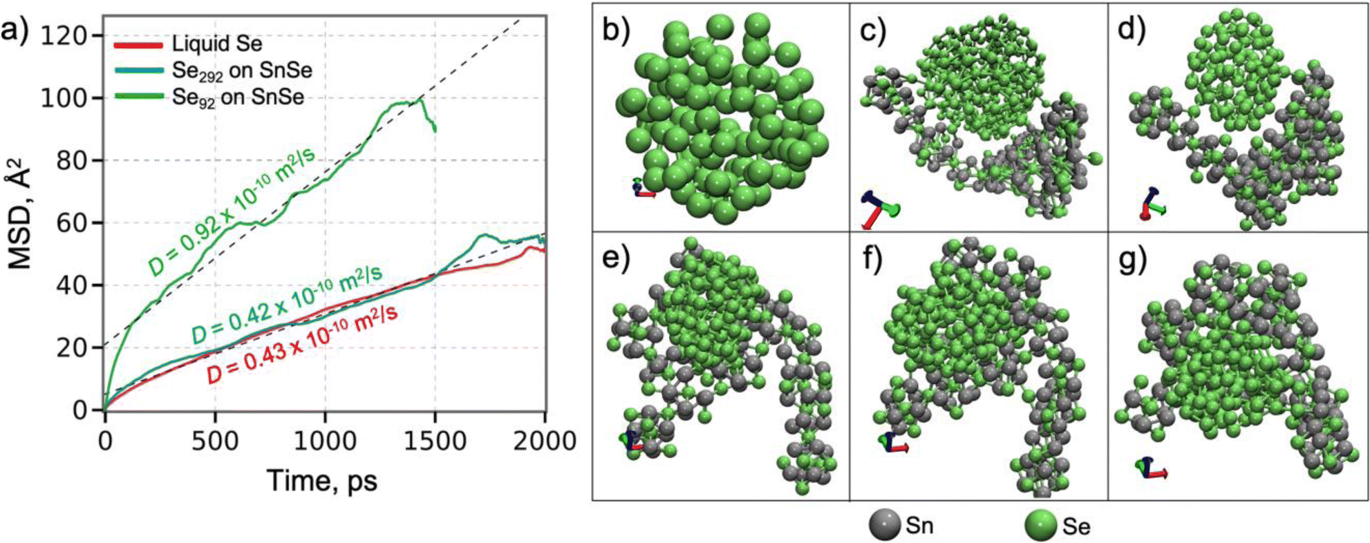 | ||
| Fig. 4 Diffusion of Se atoms in the Se cluster at 500 K. (a) The mean-square displacement as a function of time of Se atoms. Dashed lines are a linear regression of the MSD curves. (b) A free liquid Se cluster. (c) A Se292 cluster on the SnSe surface. (d) An edge-bound Se cluster. (e–g) A Se92 cluster on the SnSe surface at 96.5 ps, 289.6 ps and 407.5 ps, respectively. | ||
Overall, the ReaxFF simulations provide critical insight into the initial stages of phase formation and growth of SnSe at time scales and size scales that are not readily accessible by experiment. The ReaxFF results indicate that during the initial stages of growth there are multiple compositions and polymorphs of tin selenide forming simultaneously in the presence of dynamic selenium clusters eventually stabilizing into SnSe. The nucleation of SnSe from one of these other phases or polymorphs could lead to changes in the preferred orientation, disrupting lateral growth. To further corroborate these theory results, Raman spectroscopy was taken on films grown at 280 ± 5 °C with a 1:4 Sn:Se flux ratio captured at different growth times as shown in Fig. 5. The Raman spectra for the SnSe samples grown for longer than 5400 seconds show a clear response that matches SnSe with all the known modes present: A1g = 30 cm−1A2g = 70 cm−1; B3g = 107 cm−1, A3g = 130 cm−1; A4g = 153 cm−1. These Raman modes were confirmed by scanning a fresh 5 N SnSe single crystal (Fig. S7†). The A2g and A4g modes correspond to out-of-plane atomic vibrations while the B3g and A3g.52,53 The outlier is the peak at 185 cm−1, which has previously been attributed to the trigonal Pm1 SnSe2.54 This peak decreases in relative and total intensity to the Pmna modes as the growth continues. This SnSe2 peak is the first to form and is observed in almost every trial duration, meaning that it is likely growing prior to (or at the same time as) the Pnma phase. Taken together, the theory, Raman, and XPS results suggest that SnSe2 formation is either transient, forming first and then transitioning into SnSe over time or limited to the initial stages of growth after which the material becomes dominated by the 1:1 stoichiometry as shown in the ReaxFF model.
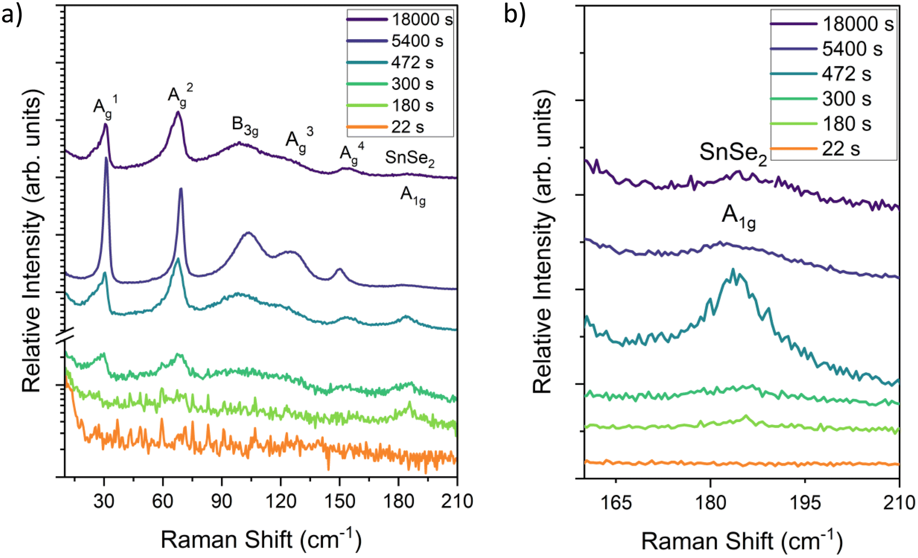 | ||
| Fig. 5 Raman spectra of Pnma SnSe thin films taken for different deposition times across (a) the full range of vibrational modes and (b) focused on the region indicating the SnSe2 A1g mode. | ||
The crystal structure and orientation of SnSe and the presence of SnSe2 are further substantiated by HAADF STEM investigation as shown in Fig. 6 on a film deposited at 270 °C using a 1:4 flux ratio at a growth rate of approximately 0.25 Å s−1 on MgO in the [100] zone axis of the substrate. For this sample, the in situ substrate anneal was forgone to promote increased surface roughness as a means to exaggerate and capture the formation of SnSe2. Throughout the film there are regions with smooth film growth of SnSe, indicated in Fig. 6a. The high-resolution image of one of these regions in Fig. 6b confirms (100)-oriented, 2D layered SnSe growth on top of the highly crystalline MgO substrate. The dashed rectangle in Fig. 6b highlights the atomic arrangement in the MgO with enhanced contrast for ease of visibility. The measured spacing in the film is consistent with the atomic spacing along the out-of-plane direction in SnSe. With a lattice constant of 1.135 nm and 4 atomic layers per unit cell, then the individual layer spacing is 0.284 nm, consistent to the spacing measured from the STEM images.40 These results are also supported by EDS measurements showing a 1:1 ratio SnSe in this region. Within the SnSe film in Fig. 6b, furthermore, two different atomic in-plane arrangements are present. The 14 layers of SnSe closest to the substrate were identified as (100)-oriented SnSe in the [012] zone axis on which a thicker region of (100)-oriented SnSe in the [011] zone axis can be seen. The respective zone axes in the SnSe are indicated in Fig. 6b and their boundary is highlighted by a black dashed line. This direct observation of misoriented in-plane domains in the SnSe film is in agreement with the conclusions derived from RHEED in Fig. 2. These results correspond with the XRD data showing predominantly the basal plane oriented out-of-plane (a-axis) in thicker films. Additionally, there is an amorphous region at the interface between the film and substrate. This amorphous region likely stems from the polycrystalline defects, misfit dislocations, and surface hydroxyl layers that are well known to form on the surface of MgO.55,56 These issues are mitigated with in situ vacuum annealing, which is discussed in the methods section. Given that (100)-oriented SnSe thin films can form atop these amorphous structures suggests that substrate templating is not required for the stabilization of the out-of-plane (100) Pnma orientation. However, although the substrate is believed to play only a marginal role in 2D van der Waals epitaxy, it might still crucially influence the orientation of the film. Interspersed throughout this same film in Fig. 6a are also regions with layer spacing that does not fit with the structure of SnSe. Fig. 6c provides an example of one of these regions. The average interatomic spacing measured in the indicated region in Fig. 6c is 0.33 nm, which is consistent with previous reports of the layer spacing in SnSe2.44 These regions predominately occur near the interface with the substrate and at specific out-of-plane orientations. The fast Fourier transform (fft) electron diffraction pattern from the indicated region in Fig. 6c is shown in Fig. 6d and fits indeed with the diffraction pattern of (![[1 with combining macron]](https://www.rsc.org/images/entities/char_0031_0304.gif) 2)-oriented SnSe2in the [432] zone axis.57 This further supports the hypothesis that alongside SnSe a certain percentage of SnSe2 forms in the film. SnSe2 might form before SnSe and the small SnSe2 regions observed in Fig. 6 might be remnants due to the increased surface roughness in this particular sample. Previous literature has shown the stabilization of SnSe/SnSe2/SnO2 heterostructures when annealing SnSe in the presence of oxygen.58 In this structure, SnSe2 and SnSe maintained an epitaxial relationship through a shared layer of slightly distorted selenium, while the surface oxide was randomly oriented. Since the films in this work are deposited onto oxide surfaces, this relationship is likely inverted (oxide–SnOx–SnSe2–SnSe).
2)-oriented SnSe2in the [432] zone axis.57 This further supports the hypothesis that alongside SnSe a certain percentage of SnSe2 forms in the film. SnSe2 might form before SnSe and the small SnSe2 regions observed in Fig. 6 might be remnants due to the increased surface roughness in this particular sample. Previous literature has shown the stabilization of SnSe/SnSe2/SnO2 heterostructures when annealing SnSe in the presence of oxygen.58 In this structure, SnSe2 and SnSe maintained an epitaxial relationship through a shared layer of slightly distorted selenium, while the surface oxide was randomly oriented. Since the films in this work are deposited onto oxide surfaces, this relationship is likely inverted (oxide–SnOx–SnSe2–SnSe).
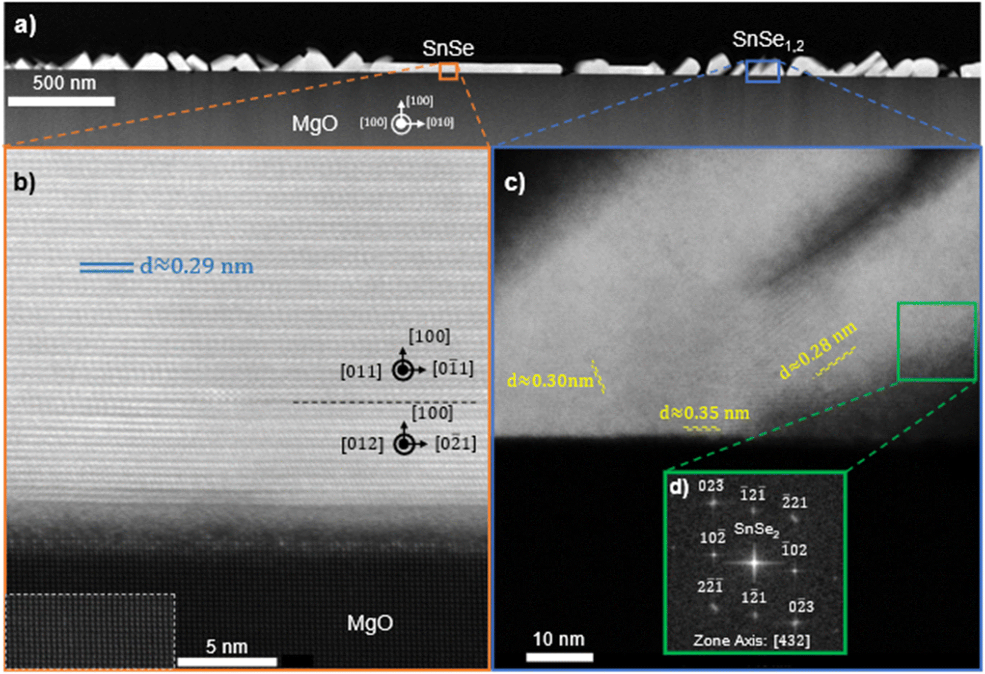 | ||
| Fig. 6 HAADF STEM images of SnSe film on MgO at a 1:4 Sn:Se flux ratio at 270 °C for 6 hours at (a) the interface between MgO and SnSe highlighting both flat in-plane growths and angled out-of-plane structures; a magnified image of (b) a region with (200) out-of-plane orientation and (c) a region with a (210) out-of-plane orientation (a); (d) an SAED pattern of a region of SnSe2. The region in the dashed white box is a high contrast section of (a) to better illustrate the cubic MgO. | ||
The impact of the presence of a tin oxide depends on the application of interest. For a through thickness piezoelectric device, it could serve as a top contact, but it would likely have a detrimental effect on the measurements of the piezoelectricity of lateral piezoelectric devices made from {200} oriented thin films of monolayer SnSe. Tin oxide layers could also function as electrodes toward a potential photovoltaic devices.59
STEM and AFM results provide insight into how to promote the lateral growth and layer control of stoichiometric SnSe. Decreasing the growth rate to 0.16 nm min−1 at 280 ± 5 °C over a 30-minute span gave rise to large lateral regions with a 0.6 nm step height, matching the lattice spacing for monolayer SnSe. These results are shown in the AFM plot in Fig. 7. There is a broad base layer of SnSe that extends micrometers laterally, although not continuously. Small gaps in the SnSe film expose the MgO substrate.
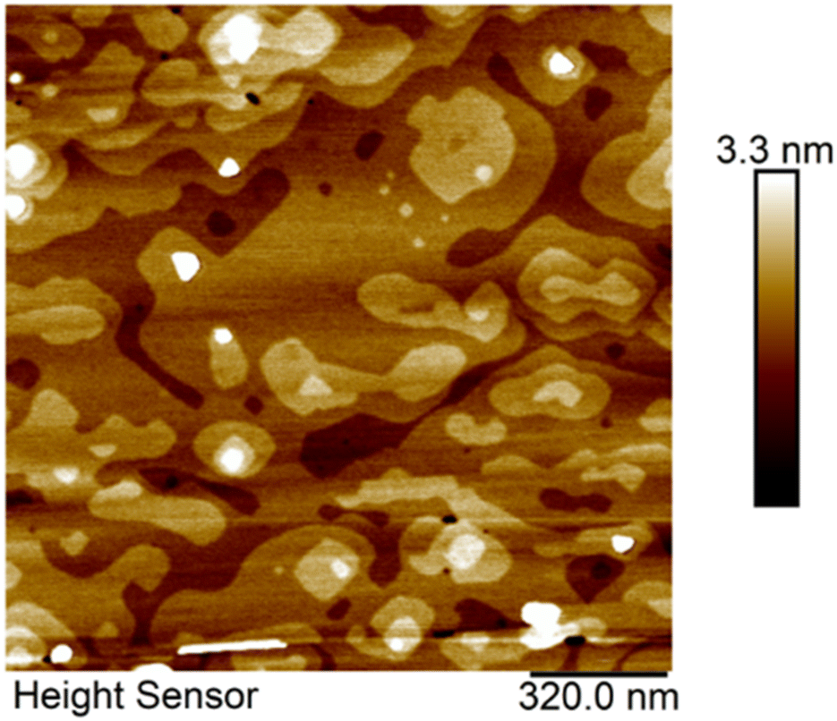 | ||
| Fig. 7 SnSe thin film grown on MBE at 285 °C for 30 min. There are large lateral regions. The step height between islands is approximately 0.6 nm which matches the monolayer of SnSe. | ||
The increased lateral growth stems from the slower growth rate used in the deposition. The slower growth rate used in the deposition allowed for additional time for the Se atoms to move across the surface and bond with the in-plane sites, leading to more lateral growth. Another point of contrast is that the MgO in Fig. 7 was cleaved and vacuum-annealed, as opposed to prior samples that were only vacuum-annealed. Cleaving the substrates shortly before growth (ideally in the UHV environment) decreases the surface contamination, thereby lowering the number of heterogeneous nucleation sites and the amount of misoriented grains. There are several islands with step heights measuring 0.6 nm grow on top of the base monolayer-thin film. Further decreases in growth rate could expand the lateral scale of the base plane by reducing the formation of other tin selenide compositions and allowing for further time for the diffusion of material to the layer edge.
Collectively, the molecular dynamics models and XPS show that the stoichiometry of SnSe is self-limiting due to the weak interactions between the selenium liquid clusters and the SnSe clusters. The self-limiting stoichiometry of SnSe is a result of several mechanisms operating in tandem. The sticking coefficient of selenium at the growth temperatures is effectively zero.30 The theory results indicate that the excess selenium forms clusters that translate across the surface. These selenium clusters are weakly interacting with the SnSe film, leading to the stabilization of a 1:1 SnSe stoichiometry as film growth progresses. The excess Se therefore does not extensively contribute to the development of SnSe2. This phenomenon of self-limiting growth occurs in other systems comprised of volatile components in the presence of an excess of one constituent element, such as Bi4Ti3O12 and GaSe thin films,31,60 setting a precedent for the application of these mechanisms. Self-limiting growth provides an opportunity to enact layer control while still maintaining a 1:1 stoichiometry. The self-limiting nature of tin selenide also benefits from the low sticking coefficient of selenium at the deposition temperatures and the limited interaction between SnSe and Se clusters. Similar selenides such as GeSe and PbSe may also exhibit a similar mechanism of self-limiting stoichiometry. The vaporization temperatures of Ge and Pb are significantly higher than that of Se, which is believed to be one aspect of the self-limiting mechanism in SnSe. Also, both SnSe and GeSe are predicted to form in the Pnma space group in their ground state with similar vdW bonding as SnSe, furthering the idea that they could behave similarly under excess anion flux.61,62 Like SnSe, PbSe can form in the Pnma structure with vdW bonds between layers.62 Although this material is predicted to be slightly unstable (Ehull = 0.053 eV per atom), the similarity between SnSe and PbSe, such as vdW bonds between layers and relatively high vaporization temperature of lead compared to selenium could make this material system an interesting prospect for this self-limiting mechanism.
Tracking the impact of SnxSey phase formation on the crystallographic orientation through XRD and STEM provides useful insight for accessing other metastable polymorphs and compounds of tin selenide as well as how to promote the lateral growth of SnSe. Increasing the lateral size of the (200) oriented SnSe regions beyond 1 μm will allow for the use of standard nanofabrication processes necessary for the development of electronic or optoelectronic devices.
Conclusions
In conclusion, the Pnma phase of SnSe could be grown via molecular beam epitaxy (MBE) over a broad range of flux ratios from 1:1 to 1:5. Changing the flux ratio did not change the film stoichiometry but did change the predominant crystallographic orientation of the film from (210) to (200). ReaxFF-based molecular dynamics (MD) simulations show that both SnxSex and SnxSe2x clusters form at the beginning of growth. These results are corroborated by Raman measurements showing the formation of SnSe2 during the initial stages of growth, that later self-stabilizes into a 1:1 SnSe. SnSe2 is also observed by HAADF STEM for films growth under rapid deposition on rough substrates, leading to changes in the crystallographic orientation of the SnSe films. As cluster size evolves, the MD results show that the core of the cluster stabilizes to a Sn:Se ratio of 1:1. The MD models show that the excess selenium coalesces into Se clusters that weakly interact with the surface of the SnSe particles, leading to the limited stoichiometric change. Additionally, the structure of the SnSe cluster is quite insensitive to the initial molecular sizes of the Sn and Se precursors. These results provide a deeper understanding of the tin and selenium interactions and kinetics that lead to self-limiting stoichiometries in SnSe. Building upon the model and experimental results, the conditions for expanding lateral growth were determined to be a growth rate to 0.16 nm min−1 at 280 ± 5 °C with a 1:4 Sn:Se flux ratio on cleaved and vacuum annealed (100) MgO. Overall, we have identified a promising avenue for the growth of large lateral-scale SnSe for future device fabrication.
Author contributions
Thin film growth was conducted by J. R. C., M. B. F., D. S.-H. L., M. H. and L. M. G.; XPS analysis was conducted by J. S., J. R. C., M. B. F., and I. C. G. TEM characterization was conducted by K. W.; Raman, ToF-SIMs, RHEED, and AFM were taken by M. B. F., J. R. C., and L. M. G.; M. W., Y. K. S., N. N., and A. v. D. formulated the theory and ran the calculations; R. E.-H., M. H., and L. M. G. coordinated the work. The paper was written by L. M. G., J. R. C., I. C. G. and M. B. F., with contributions from all authors. All authors approve of this work.Conflicts of interest
There are no conflicts to declare.Acknowledgements
The work presented has been facilitated by the Materials Innovation Platform of The Pennsylvania State University, i.e., the Two-Dimensional Crystal Consortium (2DCC-MIP) supported by NSF through cooperative agreements no. DMR-1539916 and DMR-2039351. DSHL acknowledges the support of the center for 3D Ferroelectric Microelectronics (3DFeM), an Energy Frontier Research Center funded by the U.S. Department of Energy, Office of Science, Office of Basic Energy Sciences Energy Frontier Research Centers program under Award Number DE-SC0021118. JC acknowledges the support of the National Science Foundation (NSF) Graduate Research Fellowship Program under Grant No. DGE-2039655. JC, MF, and LMG acknowledge the Air Force Office of Scientific Research (AFOSR) Young Investigator Award under Grant No. AWD-003701.References
- Y. Wu, W. Yuan, M. Xu, S. Bai, Y. Chen, Z. Tang, C. Wang, Y. Yang, X. Zhang, Y. Yuan, M. Chen, X. Zhang, B. Liu and L. Jiang, Chem. Eng. J., 2021, 412, 128744 CrossRef CAS.
- M. Chhowalla, H. S. Shin, G. Eda, L.-J. Li, K. P. Loh and H. Zhang, Nat. Chem., 2013, 5, 263–275 CrossRef PubMed.
- T. Akamatsu, T. Ideue, L. Zhou, Y. Dong, S. Kitamura, M. Yoshii, D. Yang, M. Onga, Y. Nakagawa, K. Watanabe, T. Taniguchi, J. Laurienzo, J. Huang, Z. Ye, T. Morimoto, H. Yuan and Y. Iwasa, Science, 2021, 372, 68–72 CrossRef CAS PubMed.
- G. Z. Magda, J. Pető, G. Dobrik, C. Hwang, L. P. Biró and L. Tapasztó, Sci. Rep., 2015, 5, 14714 CrossRef CAS PubMed.
- L. C. Gomes, A. Carvalho and A. H. Castro Neto, Phys. Rev. B: Condens. Matter Mater. Phys., 2015, 92, 214103 CrossRef.
- K. Chang, F. Küster, B. J. Miller, J.-R. Ji, J.-L. Zhang, P. Sessi, S. Barraza-Lopez and S. S. P. Parkin, Nano Lett., 2020, 20, 6590–6597 CrossRef CAS PubMed.
- Z. Hu, Y. Ding, X. Hu, W. Zhou, X. Yu and S. Zhang, Nanotechnology, 2019, 30, 252001 CrossRef CAS PubMed.
- C. Cui, F. Xue, W.-J. Hu and L.-J. Li, npj 2D Mater. Appl., 2018, 2, 1–14 CrossRef.
- L. V. Titova, B. M. Fregoso and R. L. Grimm, in Chalcogenide, Elsevier, 2020, pp. 119–151 Search PubMed.
- M. Zhu, M. Zhong, X. Guo, Y. Wang, Z. Chen, H. Huang, J. He, C. Su and K. P. Loh, Adv. Opt. Mater., 2021, 9, 2101200 CrossRef CAS.
- T. Hu and J. Dong, Phys. Chem. Chem. Phys., 2016, 18, 32514–32520 RSC.
- N. R. Alluri, N. P. M. J. Raj, G. Khandelwal and S.-J. Kim, Nano Energy, 2021, 88, 106231 CrossRef CAS.
- R. Carter, M. Suyetin, S. Lister, M. A. Dyson, H. Trewhitt, S. Goel, Z. Liu, K. Suenaga, C. Giusca, R. J. Kashtiban, J. L. Hutchison, J. C. Dore, G. R. Bell, E. Bichoutskaia and J. Sloan, Dalton Trans., 2014, 43, 7391–7399 RSC.
- M. Kumar, S. Rani, Y. Singh, K. Singh Gour and V. Nand Singh, RSC Adv., 2021, 11, 6477–6503 RSC.
- Y. Zhong, L. Zhang, V. Linseis, B. Qin, W. Chen, L.-D. Zhao and H. Zhu, Nano Energy, 2020, 72, 104742 CrossRef CAS.
- W.-Z. Fang, Z. Lichuan, G. Qin, Q.-B. Yan, Q. Zheng and G. Su, arXiv, 2016, 1603.01791.
- H.-Y. Song and J.-T. Lü, Chem. Phys. Lett., 2018, 695, 200–204 CrossRef CAS.
- N. Higashitarumizu, H. Kawamoto, M. Nakamura, K. Shimamura, N. Ohashi, K. Ueno and K. Nagashio, Nanoscale, 2018, 10, 22474–22483 RSC.
- W. Shi, M. Gao, J. Wei, J. Gao, C. Fan, E. Ashalley, H. Li and Z. Wang, Adv. Sci., 2018, 5, 1700602 CrossRef PubMed.
- Z. Wang and F. Pang, Chem. Phys. Lett., 2018, 702, 90–95 CrossRef CAS.
- J. Z. Jian Zhang, H. Zhu, X. Wu, H. Cui, D. Li, J. Jiang, C. Gao, Q. Wang and Q. Cui, Nanoscale, 2015, 7, 10807–10816 RSC.
- Y. Zhang, Y. Shi, M. Wu, K. Zhang, B. Man and M. Liu, Nanomaterials, 2018, 8, 515 CrossRef PubMed.
- V. Q. Nguyen, J. Kim and S. Cho, J. Korean Phys. Soc., 2018, 72, 841–857 CrossRef CAS.
- J. Jiang, C. P. Y. Wong, J. Zou, S. Li, Q. Wang, J. Chen, D. Qi, H. Wang, G. Eda, D. H. C. Chua, Y. Shi, W. Zhang and A. T. S. Wee, 2D Mater., 2017, 4, 021026 CrossRef.
- K. Chang and S. S. P. Parkin, J. Appl. Phys., 2020, 127, 220902 CrossRef CAS.
- M. R. Barone, M. Jeong, N. Parker, J. Sun, D. A. Tenne, K. Lee and D. G. Schlom, APL Mater., 2022, 10, 091106 CrossRef CAS.
- L. M. Garten, Z. Jiang, H. Paik, J. D. Perkins, A. Kakekhani, R. Fei, D. J. Werder, M. E. Holtz, D. S. Ginley, A. M. Rappe, D. G. Schlom and M. L. Staruch, Chem. Mater., 2021, 33, 7423–7431 CrossRef CAS.
- M. A. Franzman, C. W. Schlenker, M. E. Thompson and R. L. Brutchey, J. Am. Chem. Soc., 2010, 132, 4060–4061 CrossRef CAS PubMed.
- X.-H. Ma, K.-H. Cho and Y.-M. Sung, CrystEngComm, 2014, 16, 5080–5086 RSC.
- D. S. H. Liu, M. Hilse and R. Engel-Herbert, J. Vac. Sci. Technol., A, 2022, 40, 053407 CrossRef CAS.
- S. Migita, H. Ota, H. Fujino, Y. Kasai and S. Sakai, J. Cryst. Growth, 1999, 200, 161–168 CrossRef CAS.
- V. Q. Nguyen, V. T. Duong, T. H. Nguyen, R. Kang, A. T. Pham, V. T. Tran, C. K. Nguyen, A. T. Duong, T. B. Phan, J. Kim and S. Cho, J. Alloys Compd., 2020, 840, 155680 CrossRef CAS.
- T. Katase, Y. Takahashi, X. He, T. Tadano, K. Ide, H. Yoshida, S. Kawachi, J. Yamaura, M. Sasase, H. Hiramatsu, H. Hosono and T. Kamiya, Sci. Adv., 2021, 7, eabf2725 CrossRef CAS PubMed.
- A. C. T. van Duin, S. Dasgupta, F. Lorant and W. A. Goddard, J. Phys. Chem. A, 2001, 105, 9396–9409 CrossRef CAS.
- T. P. Senftle, S. Hong, M. M. Islam, S. B. Kylasa, Y. Zheng, Y. K. Shin, C. Junkermeier, R. Engel-Herbert, M. J. Janik, H. M. Aktulga, T. Verstraelen, A. Grama and A. C. T. van Duin, npj Comput. Mater., 2016, 2, 1–14 CrossRef.
- A. C. T. van Duin, J. M. A. Baas and B. van de Graaf, J. Chem. Soc., Faraday Trans., 1994, 90, 2881–2895 RSC.
- J. Gainza, F. Serrano-Sánchez, J. E. F. S. Rodrigues, Y. Huttel, O. J. Dura, M. M. Koza, M. T. Fernández-Díaz, J. J. Meléndez, B. G. Márkus, F. Simon, J. L. Martínez, J. A. Alonso and N. M. Nemes, Cell Rep. Phys. Sci., 2020, 1, 100263 CrossRef CAS.
- H. Soon Im, Y. Myung, Y. Cho, C. Kim, H. Kim, S. Back, C. Jung, D. M. Jang, Y. Lim, J. Park and J.-P. Ahn, RSC Adv., 2013, 3, 10349 RSC.
- D. Grier, G. McCarthy, D. Seidler and P. Boudjouk, Grant–Aid.
- H. Swanson, R. Fuyat and G. Ugrinic, Natl. Bur. Stand., 1953, 1(24), 539 Search PubMed.
- Y. Li, B. He, J. P. Heremans and J.-C. Zhao, J. Alloys Compd., 2016, 669, 224–231 CrossRef CAS.
- M. Wołcyrz, R. Kubiak and S. Maciejewski, Phys. Status Solidi B, 1981, 107, 245–253 CrossRef.
- A. Monshi, M. R. Foroughi and M. R. Monshi, World J. Nano Sci. Eng., 2012, 2, 154–160 CrossRef.
- G. Busch, C. Fröhlich and F. Hulliger, Helv. Phys. Acta, 1961, 34, 359–368 CAS.
- Z. V. Borges, C. M. Poffo, J. C. de Lima, S. M. Souza, D. M. Trichês and R. S. de Biasi, J. Appl. Phys., 2018, 124, 215901 CrossRef.
- Z. Wang, J. Wang, Y. Zang, Q. Zhang, J.-A. Shi, T. Jiang, Y. Gong, C.-L. Song, S.-H. Ji, L.-L. Wang, L. Gu, K. He, W. Duan, X. Ma, X. Chen and Q.-K. Xue, Adv. Mater., 2015, 27, 4150–4154 CrossRef CAS PubMed.
- B. D. Tracy, X. Li, X. Liu, J. Furdyna, M. Dobrowolska and D. J. Smith, J. Cryst. Growth, 2016, 453, 58–64 CrossRef CAS.
- W. Jin, S. Vishwanath, J. Liu, L. Kong, R. Lou, Z. Dai, J. T. Sadowski, X. Liu, H.-H. Lien, A. Chaney, Y. Han, M. Cao, J. Ma, T. Qian, J. I. Dadap, S. Wang, M. Dobrowolska, J. Furdyna, D. A. Muller, K. Pohl, H. Ding, H. G. Xing and J. Osgood, Phys. Rev. X, 2017, 7, 041020 Search PubMed.
- C. C. Miller and J. Walker, Proc. R. Soc. London, Ser. A, 1924, 106, 724–749 CAS.
- W. A. Phillips, U. Buchenau, N. Nücker, A.-J. Dianoux and W. Petry, Phys. Rev. Lett., 1989, 63, 2381–2384 CrossRef CAS PubMed.
- A. Axmann, W. Gissler, A. Kollmar and T. Springer, Discuss. Faraday Soc., 1970, 50, 74–81 RSC.
- L. Hao, Y. Du, Z. Wang, Y. Wu, H. Xu, S. Dong, H. Liu, Y. Liu, Q. Xue, Z. Han, K. Yan and M. Dong, Nanoscale, 2020, 12, 7358–7365 RSC.
- P. Li, Z. Zhang, W. Shen, C. Hu, W. Shen and D. Zhang, J. Mater. Chem. A, 2021, 9, 4716–4723 RSC.
- X. Gong, Y. Wang, Q. Hong, J. Liu, C. Yang, H. Zou, Y. Zhou, D. Huang, H. Wu, Z. Zhou, B. Zhang and X. Zhou, Spectrochim. Acta, Part A, 2022, 265, 120375 CrossRef CAS PubMed.
- T. Wagner and M. Rühle, MRS Online Proc. Libr., 1994, 357, 41–46 CrossRef.
- H. Zhou, H.-Q. Wang, Y. Li, K. Li, J. Kang, J.-C. Zheng, Z. Jiang, Y. Huang, L. Wu, L. Zhang, K. Kisslinger and Y. Zhu, ACS Appl. Mater. Interfaces, 2014, 6, 13823–13832 CrossRef CAS PubMed.
- X. Zhou, L. Gan, W. Tian, Q. Zhang, S. Jin, H. Li, Y. Bando, D. Golberg and T. Zhai, Adv. Mater., 2015, 27, 8035–8041 CrossRef CAS PubMed.
- B. Zhang, A. Li, G. Han, Z. Zhang, K. Peng, X. Gong, X. Zhou and X. Han, ACS Appl. Mater. Interfaces, 2020, 12(24), 27700–27707 CAS.
- A. Zatirostami, Mater. Sci. Semicond. Process., 2021, 135, 106044 CrossRef CAS.
- C. H. Lee, S. Krishnamoorthy, D. J. O'Hara, M. R. Brenner, J. M. Johnson, J. S. Jamison, R. C. Myers, R. K. Kawakami, J. Hwang and S. Rajan, J. Appl. Phys., 2017, 121, 094302 CrossRef.
- Z. Muhammad, Y. Li, G. Abbas, M. Usman, Z. Sun, Y. Zhang, Z. Lv, Y. Wang and W. Zhao, Adv. Electron. Mater., 2022, 8, 2101112 CrossRef CAS.
- V. L. Deringer, R. P. Stoffel and R. Dronskowski, Phys. Rev. B: Condens. Matter Mater. Phys., 2014, 89, 094303 CrossRef.
Footnote |
| † Electronic supplementary information (ESI) available. See DOI: https://doi.org/10.1039/d3nr00645j |
| This journal is © The Royal Society of Chemistry 2023 |