
 Open Access Article
 This Open Access Article is licensed under a Creative Commons Attribution-Non Commercial 3.0 Unported Licence
Large area inkjet-printed metal halide perovskite LEDs enabled by gas flow assisted drying and crystallization†
Vincent R. F.
Schröder
 a,
Nicolas
Fratzscher
b,
Florian
Mathies
c,
Edgar R.
Nandayapa
a,
Felix
Hermerschmidt
*b,
Eva L.
Unger
cde and
Emil J. W.
List-Kratochvil
*ab
a,
Nicolas
Fratzscher
b,
Florian
Mathies
c,
Edgar R.
Nandayapa
a,
Felix
Hermerschmidt
*b,
Eva L.
Unger
cde and
Emil J. W.
List-Kratochvil
*ab
aHelmholtz-Zentrum Berlin für Materialien und Energie, Hahn-Meitner-Platz 1, 14109 Berlin, Germany. E-mail: emil.list-kratochvil@hu-berlin.de
bInstitut für Physik, Institut für Chemie, IRIS Adlershof, Humboldt-Universität zu Berlin, Zum Großen Windkanal 2, 12489 Berlin, Germany. E-mail: felix.hermerschmidt@hu-berlin.de
cDepartment Solution Processing of Hybrid Materials & Devices, Helmholtz-Zentrum Berlin für Materialien und Energie, Kekuléstraße 5, 12489 Berlin, Germany
dHybrid Materials: Formation and Scaling, IRIS Adlershof, Humboldt-Universität zu Berlin, Am Großen Windkanal 2, 12489 Berlin, Germany
eChemical Physics and NanoLund, Lund University, PO Box 124, 22100 Lund, Sweden
First published on 23rd February 2023
Abstract
We demonstrate the upscaling of inkjet-printed metal halide perovskite light-emitting diodes. To achieve this, the drying process, critical for controlling the crystallization of the perovskite layer, was optimized with an airblade-like slit nozzle in a gas flow assisted vacuum drying step. This yields large, continuous perovskite layers in light-emitting diodes with an active area up to 1600 mm2.
Introduction
Metal halide perovskites (MHPs) have attracted much attention from researchers in academia and industry alike for their promising performance in optoelectronic devices, such as solar cells,1,2 photodetectors,3,4 X-ray detectors,5,6 and light-emitting diodes (LEDs).7–9 MHPs are a solution-processable class of crystalline semiconductors and as such a promising candidate for high-performance printed (opto)electronics.The soluble nature of MHPs allows for cheap and fast fabrication by spin coating, slot-die coating or inkjet printing. Inkjet printing in particular is a high-throughput, large area, and selective deposition technique with industrial maturity.10 Inkjet-printed perovskite layers have been demonstrated in high-performance solar cells11–13 and in 2020 we presented the first inkjet-printed perovskite LED.14 As perovskite devices move towards commercialization, operational stability, scalable deposition techniques and processing methods become the focus of applied research. MHP solar cells currently suffer from a strong performance roll-off with increasing size of the active area.15,16 Large area metal halide perovskite LEDs (PeLEDs) have been fabricated by blade coating,17 thermal evaporation18 and spin coating,19 but not yet by inkjet printing. The fabrication of large area PeLEDs for display and solid state lighting applications is currently limited by the homogeneity of the emitter layer.20
Here, we present a successful upscaling process for inkjet-printed PeLEDs, building on previous work.14 The technical side of the inkjet printing process, meaning the specific deposition of ink on a substrate, is easily scalable and only limited by the printable dimensions of the inkjet printer being used. However, after deposition of the perovskite ink and the formation of a closed wet film, the drying and crystallization process sets in. This is a critical step in the inkjet printing process of MHPs as it determines the homogeneity of the layer thickness, its roughness and potential number of pinholes; with the target being a homogeneous and smooth perovskite layer.
The crystallization process can be controlled by temperature,21,22 vacuum treatment,23,24 or drying in a gas flow.25–27 We have previously presented a gas flow assisted vacuum drying chamber to achieve precise control over the sample environment after printing and increase the performance of inkjet-printed perovskite solar cells.28 After initial evacuation of an aluminium chamber, a controlled nitrogen-flow was released in the chamber, which initiated the gas flow assisted drying (GAVD) process of the as-deposited wet film. For this work, we have now scaled and optimized the gas flow in this chamber with a 3D printed, airblade-like slit nozzle to enable fast and homogeneous drying of a 50 × 50 mm2 substrate. The size of the active area of the inkjet-printed PeLEDs was thereby increased from the previously published 4 mm2 to 1600 mm2.
Results
The overall printing process consists of two steps. In the first step (Fig. 1a), the ink is deposited with an industrial scale R&D inkjet printer. The size of the deposited area is determined by the digital image fed into the printer software. In the second step (Fig. 2b), the as-deposited wet film is dried using a closed aluminium chamber, which provides a nitrogen gas flow under reduced pressure to dry the wet film and facilitate the crystallization of the perovskite layer (Fig. 1b).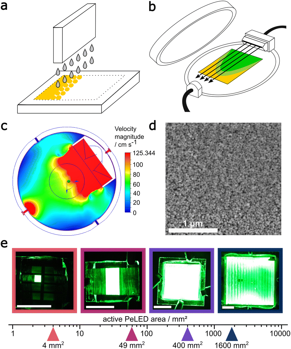 | ||
| Fig. 1 (a) Inkjet printing in combination with (b) an airblade-like gas flow, shown by (c) flow simulations, yields (d) a homogeneous perovskite morphology visible in SEM and produces (e) bright PeLEDs with an active area between 4 mm2 and 1600 mm2. The white scale bar in (e) equals 10 mm. | ||
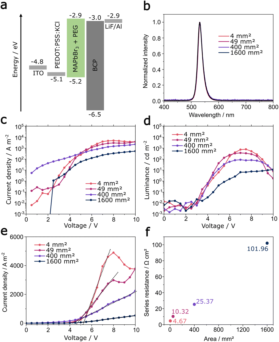 | ||
| Fig. 2 (a) Device architecture and energy levels as used previously in ref. 14, (b) electroluminescence spectra, (c) current densities, (d) luminance–voltage characteristics for all devices, (e) extraction of series resistance and (f) active area dependent series resistance. | ||
In the original design,28 an unguided gas flow hit the substrate in the centre of the GAVD-chamber (Fig. S1a†). This approch works well enough up to a substrate size of 25 × 25 mm2, but larger device areas do not show emission on the full active area due to uneven drying of the layer. For drying of larger substrates, the chamber was improved by adding a 3D printed, airblade-like slit nozzle. This nozzle, while maintaining the diameter of the nitrogen inlet cross-section, has a 70 mm wide and ∼0.5 mm high slit opening. Through this slit nozzle, the nitrogen flow retains a constant velocity over its full width, which we modelled by gas flow simulations of the process (Fig. 1c). By comparing the simulated gas flow for the original chamber design and the chamber with the slit-nozzle (Fig. S1†), we find that using the slit nozzle results in an overall reduced speed of the nitrogen flow, which in turn hits the centre of the chamber (indicated by a 50 mm ring) as a broad front. This airblade-like stream over the substrate results in a homogeneous perovskite layer with a crystal size smaller than 100 nm (Fig. 1d). Scanning electron microscope (SEM) images were additionally taken over a 1 cm2 area to show homogeneous morphology over a large area (Fig. S2†).
Using this process, we fabricated PeLEDs with a MAPbBr3:PEG emitting layer and an active area of 4mm2, 49 mm2, 400 mm2 and 1600 mm2, increasing the active area size by three orders of magnitude and allowing us to fabricate PeLEDs up to a substrate size of 50 × 50 mm2. Photos of representative devices under operation are shown in Fig. 1e. The inkjet printing process proved to be reliable independent of the substrate size, even though an inhomogeneous emission of the 1600 mm2 device at 9 V can be seen in Fig. 1e. This is not the result of a suboptimal drying process but of the high series resistance of the ITO electrode, as will be discussed later.
The architecture (Fig. 2a) of the PeLED devices is commonly applied in literature and is the same as in our previous publication.14 We continue to utilize potassium chloride as an additive of the PEDOT:PSS hole transport layer to control the crystallization at the PEDOT:PSS/perovskite interface. The perovskite composition (MAPbBr3) is unchanged, including the addition of poly ethylene glycol (PEG) to increase the homogeneity of the printed layer. MAPbBr3 is often used as emitter material in PeLEDs due to its bright green emission wavelength. It is highly soluble in the used solvent system and thus provides a large processing window to influence drying and crystallization after deposition. X-ray diffraction measurements (Fig. S3†) confirm the cubic perovskite phase of MAPbBr3 and the electroluminescence spectrum shows the narrow, characteristic emission at 530 nm (Fig. 2b) being identical for all devices.
The current density–voltage (J–V) characteristics of the PeLEDs reveal a decreasing current density with increasing active area size (Fig. 2c). The reduction in current density is accompanied by a decrease of the maximum luminance with increasing area size. The luminance–voltage (L–V) characteristics are displayed in Fig. 2d. PeLEDs with an active area of 4 mm2, 49 mm2 and 400 mm2 show a very similar trend, with a turn-on voltage (defined as the voltage at 0.1 cd m−2) of 3.4 V, a maximum luminance of 789 cd m−2, 369 cd m−2 and 88 cd m−2 at ∼7 V, respectively. Subsequently, a steep roll-off with further increase in voltage occurs, due to degradation of the emitter material. The 1600 mm2 devices show instead a less steep luminance progression after turn-on and a maximum luminance of 14 cd m−2 at 10 V.
In order to investigate this difference, we extracted the series resistance from the slope of the current density between 4 V and 8 V, as shown in Fig. 2e. We observe a linear correlation with area size (Fig. 2f), increasing from 4.76 Ω cm2 for the 4 mm2 device to 101.96 Ω cm2 for the 1600 mm2 device. The increasing series resistance is here caused by the high sheet resistance of indium-tin-oxide (ITO). This issue is well known for organic and perovskite thin film devices with a transparent conducting electrode (TCO) component. Meredith et al. modelled the power loss in organic solar cells due to large area ITO electrodes (sheet resistance of ca. 10–20 Ω □−1) and a critical electrode length of 10 mm was identified for efficient charge collection.29 In our large area devices, the current path from the two contact points to the centre of the device is 20 mm and significant power loss cannot be avoided. As a result, the brightness of the PeLED decreases in a gradient from the contacted edge towards the centre, which corresponds to the drop of voltage and current density, that was modelled before for large area organic LEDs (OLEDs).30 In our case a maximum luminance of 150 cd m−2 was observed at the sample edge compared to 14 cd m−2 in the centre (see Fig. S4†).
The high series resistance of ITO can be avoided by employing a printed Ag-grid/highly conducting PEDOT or a transparent metal electrode, as we have done previously.31,32 However, our attempts to implement these solutions have been unsuccessful due to the fast degradation of the perovskite layer caused by a reaction with the fabricated silver electrodes.33,34 To address this, we are currently developing a Au-based electrode, yet this component is not yet available for this study.
Despite these current limitations, we have found means to significantly improve the inhomogenous light emission and improve the performance of the devices by replacing the electron-transport layer (ETL) bathocuproin (BCP) by 2,2′,2′′-(1,3,5-benzinetriyl)-tris(1-phenyl-1-H-benzimidazole) (TPBi) (Fig. 3a). TPBi is a commonly used ETL for organic and perovskite light-emitting diodes and has similar energy levels to BCP but a higher electron mobility.35–37 The complete series of PeLEDs with 4 mm2, 49 mm2, 400 mm2 and 1600 mm2 active area were fabricated with TPBi as ETL. Using 20 nm TPBi enabled the fabrication of a bright, 1600 mm2 large PeLED (Fig. 3b) with homogeneous green emission at 7 V. The J–V characteristics of the respective champion devices (Fig. 3c) confirm the trend of decreasing current density with increasing active area size. As described above for the BCP devices, the decreasing current density is caused by an increasing series resistance (Fig. 2c and d). The leakage current (current density at 0–2 V) is lower than 1 A m−2 and does not increase with larger active area, demonstrating the low pinhole density of the inkjet-printed perovskite layer.
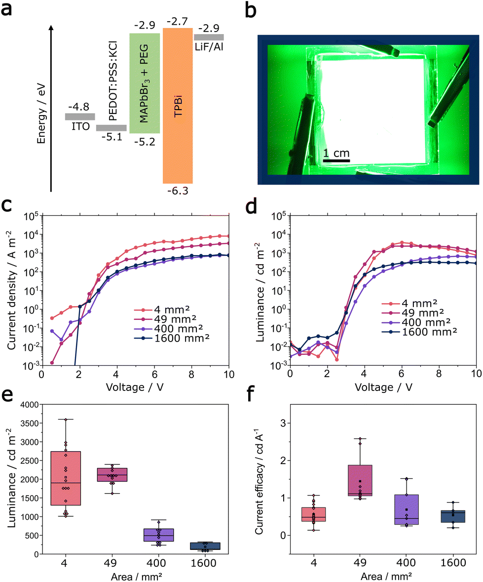 | ||
| Fig. 3 (a) Usage of a TPBi electron transport layer improves devices performance and enables (b) homogeneous emission from a 1600 mm2 PeLED. Current density–voltage (c) and luminance–voltage (d) characteristics show greatly improved performance of champion devices. The luminance distribution (e) and current efficacy distribution (f) for all fabricated devices. | ||
The change of the ETL to TPBi also significantly increased the absolute luminance of the PeLEDs, independent of area size (Fig. 3d). All devices exhibit an earlier turn-on voltage at ca. 2.8 V, compared to devices with BCP. Champion devices with an active area of 4 mm2, 49 mm2, 400 mm2 and 1600 mm2 exhibited a maximum luminance of 3598 cd m−2, 2338 cd m−2, 673 cd m−2 and 324 cd m−2, respectively. We note the reduction of the steep roll-off compared to that observed in the BCP devices. In Fig. 3e the maximum luminance of all fabricated TPBi devices is shown. PeLEDs that use TPBi as ETL outperform devices containing BCP at every active area size, i.e. 4 mm2, 49 mm2, 400 mm2 and 1600 mm2, achieving average maximum luminance values of 2046 cd m−2, 2098 cd m−2, 504 cd m−2 and 187 cd m−2 with TPBi compared to 1137 cd m−2, 660 cd m−2, 291 cd m−2 and 6 cd m−2 with BCP (shown in Fig. S5†). The higher luminance in TPBi-containing devices is due to a decreased injection barrier, which also reduces the turn-on voltage and increases the current efficacy.
Even though the nominal luminance values are reduced as the active area size increases, the proportional reduction in current density of the TPBi-containing PeLEDs is reflected in the consistent current efficacy (cd A−1) of the devices. Fig. 3f shows an average current efficacy of ca. 0.5 cd A−1 for devices with an area of 4 mm2, 400 mm2 and 1600 mm2 and 1.5 cd A−1 for 49 mm2. Specifically for the champion devices, TPBi-containing PeLEDs show a current efficacy of 0.8 to 1.0 cd A−1 at ∼2 V lower bias than BCP-containing champion devices with an area of 4 mm2, 400 mm2 and 1600 mm2, while even producing a notably high current efficacy of 2.6 cd A−1 for the 49 mm2 champion device (see Fig. S6†). Conversely, the current efficacy of BCP-containing devices reaches maximum values of 0.2 cd A−1 for 4 mm2 PeLEDs and decreases with increasing active area size to 0.03 cd A−1 for 1600 mm2.
It must be noted that replacing the ETL does not influence the series resistance or the resulting voltage drop since all devices are using ITO electrodes. The reduction of series resistance can only be addressed at a later stage. As a result, the 1600 mm2 devices with TPBi still show inhomogeneous emission at lower voltages (Fig. S7†). However, at 7 V the luminance gradient becomes imperceptable and the emission of 1600 mm2 PeLEDs using TPBi seems homogeneous over the full area.
Conclusions
We have demonstrated an upscaling process for inkjet-printed metal halide perovskite light-emitting diodes. Using a laboratory scale inkjet printer and a custom-made drying chamber with an airblade-like slit nozzle, the airflow and the drying behaviour of the inkjet-printed wet film were optimized. We successfully upscaled the existing process, achieved a large and homogeneous perovskite layer and fabricated PeLEDs with an active area size of up to 1600 mm2, with J–V characteristics showing no increase in leakage current.Upscaling the PeLEDs from 4 mm2 to 1600 mm2 was met by two challenges: (1) inhomogeneous emission of large area (1600 mm2) devices and (2) reduced device performance with larger active area size. Both phenomena are a result of increasing series resistance, due to the sheet resistance of ITO. First, the resulting voltage gradient causes a luminance gradient from the point of contact on the ITO to the centre. Second, the decreasing current density with increasing active area size is the reason for the decrease in luminance of the devices.
While the reduction of series resistance cannot be addressed at the moment, we were able to overcome the inhomogeneous emission and improve the overall device performance by replacing the ETL BCP with TPBi. In the 1600 mm2 devices we can show homogeneous emission and a luminance of over 300 cd m−2. Furthermore, the resulting current efficacy of PeLEDs with TPBi remains largely constant independent of the active area size. With this work, we have continued the development of inkjet-printed metal halide perovskite materials and provide access to large area light-emitting diodes.
Experimental
Perovskite ink preparation
The perovskite ink was prepared in a nitrogen-filled glovebox by dissolving lead bromide (>98%, TCI) and methyl ammonium bromide (99.99% trace elements basis, dyenamo) in a 3![[thin space (1/6-em)]](https://www.rsc.org/images/entities/char_2009.gif) :7:10 mixture of DMF (anhydrous, 99.9%, Sigma-Aldrich), DMSO (anhydrous, >99.9%, Sigma-Aldrich) and GBL (>99.0%, TCI) to yield a 59.87 mg mL−1 (0.125 mol L−1) solution with an excess of 5 wt% of MABr. 8 mg mL−1 of PEG was added to this solution.
:7:10 mixture of DMF (anhydrous, 99.9%, Sigma-Aldrich), DMSO (anhydrous, >99.9%, Sigma-Aldrich) and GBL (>99.0%, TCI) to yield a 59.87 mg mL−1 (0.125 mol L−1) solution with an excess of 5 wt% of MABr. 8 mg mL−1 of PEG was added to this solution.
Device fabrication
Patterned (10 × 15 mm2 and 25.4 × 25.4 mm2) and unpatterned (50 × 50 mm2) ITO substrates were purchased from Psiotec Limited. The 50 × 50 mm2 ITO substrates were patterned with a pulsed laser (1064 nm, 30 W) integrated in a PixDRO inkjet printer system. The substrates were cleaned with 1% Hellmanex III solution, acetone and isopropanol in an ultrasonic bath for 10 minutes. The substrates were subsequently treated with oxygen plasma in a Femto plasma system (Diener). PEDOT:PSS (Al4083, Heraeus) was mixed with 5 mg L−1 KCl (Sigma Aldrich) and spin-coated at 1500 rpm for 12 s and 2500 rpm at 30 s. The PEDOT:PSS layers were annealed at 220 °C for 10 min before transfer into a nitrogen filled glovebox. In the glovebox, the perovskite ink was deposited with a PixDRO LP50 (Meyer-Burger/Suess) inkjet printer fitted with Spectra SE print heads (30 pL nominal drop volume) and Dimatix cartridges (10 pL). The films were dried in a specifically designed aluminium chamber by evacuating the chamber for 10 s, reaching a base pressure of ∼1 mbar. After evacuation, a valve was opened to allow nitrogen to flow over the substrate. The nitrogen rate was defined by a valve. The crystallization of the perovskite film was observed through a window in the chamber. After full crystallization, the substrate was transferred to a hotplate and annealed at 100 °C for 10 min. Afterwards, the substrates were transferred to another nitrogen filled glovebox fitted with a thermal evaporator. 20 nm BCP or 20 nm TPBi, 1 nm LiF and 150 nm aluminium were thermally evaporated, with the overlap of ITO and aluminium electrode defining the active area of the devices. All devices were encapsulated using a commercially available epoxy (Blufixx) and hardened with a blue LED. The devices were characterized afterwards in ambient air. Overall, a hundred devices were fabricated and characterized. We report a yield of over 90% for all device sizes. For the different area sizes 85 (4 mm2), 36 (49 mm2), 15 (400 mm2) and 8 (1600 mm2) were fabricated. The luminance values for alle device can be found in Fig. 7S.†Thin film and device characterization
The PeLED devices were characterized by current density–luminance–voltage measurements using a Keithley source measurement unit 2612B, an LS160 luminance meter (Konica Minolta), a substrate holder and multiplexer (Ossila). Source measurement unit, multiplexer and candelameter were addressed with self-written software. The electroluminescence spectra were collected through an optical fibre with an HR 2000+ Ocean Optics spectrometer.Scanning electron microscope images were collected with a Zeiss GeminiSEM 500. XRD experiments were performed on a Bruker Advanced D8 in Bragg–Brentano geometry under ambient conditions with a Cu Kα X-ray source (λ = 1.5406 Å).
Conflicts of interest
There are no conflicts of interest to declare.Acknowledgements
This work was carried out in the framework of the Joint Lab GEN_FAB and with the support of the Helmholtz Innovation Lab HySPRINT. The authors would like to thank Christoph T. Koch for granting instrument access. E. L. U. acknowledges funding from the German Ministry of Education and Research (BMBF) for the Young Investigator Group Hybrid Materials Formation and Scaling (HyPerFORME) within the program “NanoMatFutur” (Grant No. 03XP0091), as well as the Helmholtz Energy Materials Foundry (HEMF).References
- A. Al-Ashouri, E. Köhnen, B. Li, A. Magomedov, H. Hempel, P. Caprioglio, J. A. Márquez, A. B. M. Vilches, E. Kasparavicius, J. A. Smith, N. Phung, D. Menzel, M. Grischek, L. Kegelmann, D. Skroblin, C. Gollwitzer, T. Malinauskas, M. Jošt, G. Matič, B. Rech, R. Schlatmann, M. Topič, L. Korte, A. Abate, B. Stannowski, D. Neher, M. Stolterfoht, T. Unold, V. Getautis and S. Albrecht, Science, 2020, 370, 1300–1309 CrossRef CAS PubMed.
- M. Saliba, J. P. Correa-Baena, C. M. Wolff, M. Stolterfoht, N. Phung, S. Albrecht, D. Neher and A. Abate, Chem. Mater., 2018, 30, 4193–4201 CrossRef CAS.
- V. R. F. Schröder, F. Hermerschmidt, S. Helper, C. Rehermann, G. Ligorio, H. Näsström, E. L. Unger and E. J. W. List-Kratochvil, Adv. Eng. Mater., 2021, 2101111, 1–7 Search PubMed.
- Y. Li, Z. F. Shi, S. Li, L. Z. Lei, H. F. Ji, D. Wu, T. T. Xu, Y. T. Tian and X. J. Li, J. Mater. Chem. C, 2017, 5, 8355–8360 RSC.
- H. Wei, Y. Fang, P. Mulligan, W. Chuirazzi, H. H. Fang, C. Wang, B. R. Ecker, Y. Gao, M. A. Loi, L. Cao and J. Huang, Nat. Photonics, 2016, 10, 333–339 CrossRef CAS.
- J. Liu, B. Shabbir, C. Wang, T. Wan, Q. Ou, P. Yu, A. Tadich, X. Jiao, D. Chu, D. Qi, D. Li, R. Kan, Y. Huang, Y. Dong, J. Jasieniak, Y. Zhang and Q. Bao, Adv. Mater., 2019, 31, 1–8 Search PubMed.
- K. Lin, J. Xing, L. N. Quan, F. P. G. de Arquer, X. Gong, J. Lu, L. Xie, W. Zhao, D. Zhang, C. Yan, W. Li, X. Liu, Y. Lu, J. Kirman, E. H. Sargent, Q. Xiong and Z. Wei, Nature, 2018, 562, 245–248 CrossRef CAS PubMed.
- N. F. Jamaludin, N. Yantara, Y. F. Ng, A. Bruno, B. K. Chandran, X. Y. Chin, K. Thirumal, N. Mathews, C. Soci and S. Mhaisalkar, J. Mater. Chem. C, 2018, 6, 2295–2302 RSC.
- C. Sun, Y. Jiang, M. Cui, L. Qiao, J. Wei, Y. Huang, L. Zhang, T. He, S. Li, H. Y. Hsu, C. Qin, R. Long and M. Yuan, Nat. Commun., 2021, 12, 1–11 CrossRef PubMed.
- Z. Zhan, J. An, Y. Wei, V. T. Tran and H. Du, Nanoscale, 2017, 9, 965–993 RSC.
- F. Mathies, E. J. W. List-Kratochvil and E. L. Unger, Energy Technol., 2020, 8, 1900991 CrossRef CAS.
- F. Mathies, H. Eggers, B. S. Richards, G. Hernandez-Sosa, U. Lemmer and U. W. Paetzold, ACS Appl. Energy Mater., 2018, 1, 1834–1839 CrossRef CAS.
- A. J. Huckaba, Y. Lee, R. Xia, S. Paek, V. C. Bassetto, E. Oveisi, A. Lesch, S. Kinge, P. J. Dyson, H. Girault and M. K. Nazeeruddin, Energy Technol., 2019, 7, 317–324 CrossRef CAS.
- F. Hermerschmidt, F. Mathies, V. R. F. Schröder, C. Rehermann, N. Z. Morales, E. L. Unger and E. J. W. List-Kratochvil, Mater. Horiz., 2020, 7, 1773–1781 RSC.
- J. Yan, T. J. Savenije, L. Mazzarella and O. Isabella, Sustainable Energy Fuels, 2022, 6, 243–266 RSC.
- T. J. Jacobsson, A. Hultqvist, A. García-Fernández, A. Anand, A. Al-Ashouri, A. Hagfeldt, A. Crovetto, A. Abate, A. G. Ricciardulli, A. Vijayan, A. Kulkarni, A. Y. Anderson, B. P. Darwich, B. Yang, B. L. Coles, C. A. R. Perini, C. Rehermann, D. Ramirez, D. Fairen-Jimenez, D. Di Girolamo, D. Jia, E. Avila, E. J. Juarez-Perez, F. Baumann, F. Mathies, G. S. A. González, G. Boschloo, G. Nasti, G. Paramasivam, G. Martínez-Denegri, H. Näsström, H. Michaels, H. Köbler, H. Wu, I. Benesperi, M. I. Dar, I. Bayrak Pehlivan, I. E. Gould, J. N. Vagott, J. Dagar, J. Kettle, J. Yang, J. Li, J. A. Smith, J. Pascual, J. J. Jerónimo-Rendón, J. F. Montoya, J. P. Correa-Baena, J. Qiu, J. Wang, K. Sveinbjörnsson, K. Hirselandt, K. Dey, K. Frohna, L. Mathies, L. A. Castriotta, M. H. Aldamasy, M. Vasquez-Montoya, M. A. Ruiz-Preciado, M. A. Flatken, M. V. Khenkin, M. Grischek, M. Kedia, M. Saliba, M. Anaya, M. Veldhoen, N. Arora, O. Shargaieva, O. Maus, O. S. Game, O. Yudilevich, P. Fassl, Q. Zhou, R. Betancur, R. Munir, R. Patidar, S. D. Stranks, S. Alam, S. Kar, T. Unold, T. Abzieher, T. Edvinsson, T. W. David, U. W. Paetzold, W. Zia, W. Fu, W. Zuo, V. R. F. Schröder, W. Tress, X. Zhang, Y. H. Chiang, Z. Iqbal, Z. Xie and E. Unger, Nat. Energy, 2022, 7, 107–115 CrossRef CAS.
- S. Chu, Y. Zhang, P. Xiao, W. Chen, R. Tang, Y. Shao, T. Chen, X. Zhang, F. Liu and Z. Xiao, Adv. Mater., 2022, 34, 1–9 Search PubMed.
- P. Du, J. Li, L. Wang, L. Sun, X. Wang, X. Xu, L. Yang, J. Pang, W. Liang, J. Luo, Y. Ma and J. Tang, Nat. Commun., 2021, 12, 1–10 CrossRef PubMed.
- X. Zhao and Z. K. Tan, Nat. Photonics, 2020, 14, 215–218 CrossRef CAS.
- Z. Ding, H. Kim, D. Lee, S. Stickel, M. Boroson, J. Hamer and N. C. Giebink, J. Appl. Phys., 2019, 125, 125 Search PubMed.
- Q. Zhou, Z. Jin, H. Li and J. Wang, Sci. Rep., 2016, 6, 1–8 CrossRef PubMed.
- P. Cui, P. Fu, D. Wei, M. Li, D. Song, X. Yue, Y. Li, Z. Zhang, Y. Li and J. M. Mbengue, RSC Adv., 2015, 5, 75622–75629 RSC.
- J. Wang, S. Gong, Z. Chen and S. Yang, ACS Appl. Mater. Interfaces, 2021, 13, 22684–22693 CrossRef CAS PubMed.
- Y. Yin, M. U. Ali, M. Liu, J. Miao, W. Peng, D. Li, S. Chen, C. Lee and H. Meng, Small, 2019, 15, 1901954 CrossRef PubMed.
- A. Babayigit, J. D'Haen, H. G. Boyen and B. Conings, Joule, 2018, 2, 1205–1209 CrossRef.
- J. Li, J. Dagar, O. Shargaieva, M. A. Flatken, H. Köbler, M. Fenske, C. Schultz, B. Stegemann, J. Just, D. M. Többens, A. Abate, R. Munir and E. Unger, Adv. Energy Mater., 2021, 11, 2003460 CrossRef CAS.
- B. Wilk, S. Sahayaraj, M. Ziółek, V. Babu, R. Kudrawiec and K. Wojciechowski, Adv. Mater. Technol., 2022, 7, 2200606 CrossRef CAS.
- F. Mathies, E. R. Nandayapa, G. Paramasivam, M. F. Al Rayes, V. R. F. Schröder, C. Rehermann, E. J. W. List-Kratochvil and E. L. Unger, Mater. Adv., 2021, 2, 5365–5370 RSC.
- P. Meredith and A. Armin, Nat. Commun., 2018, 9, 8–11 CrossRef PubMed.
- G. Burwell, N. Burridge, O. J. Sandberg, E. Bond, W. Li, P. Meredith and A. Armin, Adv. Electron. Mater., 2020, 6, 2000732 CrossRef CAS.
- L. Kinner, S. Nau, K. Popovic, S. Sax, I. Burgués-Ceballos, F. Hermerschmidt, A. Lange, C. Boeffel, S. A. Choulis and E. J. W. List-Kratochvil, Appl. Phys. Lett., 2017, 110, 110 CrossRef.
- M. Hengge, K. Livanov, N. Zamoshchik, F. Hermerschmidt and E. J. W. List-Kratochvil, Flexible Printed Electron., 2021, 6, 015009 CrossRef CAS.
- E. M. Sanehira, B. J. Tremolet De Villers, P. Schulz, M. O. Reese, S. Ferrere, K. Zhu, L. Y. Lin, J. J. Berry and J. M. Luther, ACS Energy Lett., 2016, 1, 38–45 CrossRef CAS.
- L. Zhao, R. A. Kerner, Z. Xiao, Y. L. Lin, K. M. Lee, J. Schwartz and B. P. Rand, ACS Energy Lett., 2016, 1, 595–602 CrossRef CAS.
- D. W. S. Shih-Chun Lo, N. A. H. Male, J. P. J. Markham, S. W. Magennis, P. L. Burn and O. V. Salata, Adv. Mater., 2002, 14, 975–979 CrossRef.
- E. Y. Choi, J. H. Seo, H. M. Kim, K. H. Lee, H. J. Kang, S. S. Yoon and Y. K. Kim, Jpn. J. Appl. Phys., 2011, 50, 5–8 Search PubMed.
- Y. Q. Li, M. K. Fung, Z. Xie, S. T. Lee, L. S. Hung and J. Shi, Adv. Mater., 2002, 14, 1317–1321 CrossRef CAS.
Footnote |
| † Electronic supplementary information (ESI) available. See DOI: https://doi.org/10.1039/d3nr00565h |
| This journal is © The Royal Society of Chemistry 2023 |