
Highly flexible organo-metal halide perovskite solar cells based on silver nanowire–polymer hybrid electrodes†
Han-Wen
Zhang
a,
Yan-Gang
Bi
*a,
Dong-Ming
Shan
a,
Zhi-Yu
Chen
a,
Yi-Fan
Wang
a,
Hong-Bo
Sun
 *ab and
Jing
Feng
*a
*ab and
Jing
Feng
*a
aState Key Laboratory of Integrated Optoelectronics, College of Electronic Science and Engineering, Jilin University, 2699 Qianjin Street, Changchun 130012, China. E-mail: yangang_bi@jlu.edu.cn; jingfeng@jlu.edu.cn
bState Key Laboratory of Precision Measurement Technology and Instruments, Department of Precision Instrument, Tsinghua University, Haidian, Beijing 100084, China. E-mail: hbsun@tsinghua.edu.cn
First published on 31st January 2023
Abstract
Flexible perovskite solar cells (FPSCs) have attracted considerable attention due to their broad application possibilities in next generation electronics. However, the commonly used transparent conductive electrodes (TCEs), such as indium tin oxide (ITO), suffer from poor flexible performance, impeding the development of FPSCs. Here, we propose a hybrid electrode (PUA/AgNWs/PH1000) comprising a thin percolation network of silver nanowires (AgNWs) inlaid on the surface of a flexible substrate (PUA) modified with a conductive layer (PH1000), which exhibits high optical transmittance and electrical conductivity, as well as robust mechanical flexibility. By applying the proposed PUA/AgNWs/PH1000 hybrid electrode in FPSCs, the resulting ITO-free devices exhibit the desired flexibility and mechanical stability; it can survive repeated continuous bending cycles and retain 77.4% of its initial power conversion efficiency after 10![[thin space (1/6-em)]](https://www.rsc.org/images/entities/char_2009.gif) 000 bending cycles with the bending radius of 5 mm.
000 bending cycles with the bending radius of 5 mm.
1. Introduction
Over the past decade, organic–inorganic halide perovskite solar cells have undergone rapid development, with an increased power conversion efficiency (PCE) from the initial 3.8%1 to the currently certified 25.7%,54 which is comparable to the level of commercial silicon-based solar cells.54 With the requirement of cutting-edge electronic technologies, the transition of rigid devices to flexible devices is essential, for which great efforts have been devoted to solar cells,2–5 light-emitting diodes,6–9 sensors,10,11 and photo-detectors.12–15 Particularly, flexible perovskite solar cells (FPSCs) have received considerable attention as powerful energy supply devices with broad application possibilities. However, the efficiency of FPSCs still lags behind that of rigid counterparts,16–18 which is attributed to the varying morphology and limited electrical and optical properties of the flexible substrates and electrodes.19,20As the most fundamental component, flexible transparent electrodes, with high optical transmittance and electrical conductivity, a smooth and uniform surface morphology, an appropriate work function, a simple preparation method, and good mechanical stability, play an important part in the successful development of flexible electronic devices. Transparent conductive oxides (TCOs), such as indium-doped tin oxide (ITO) and fluorine-doped tin oxide (FTO), are the most commonly used transparent electrodes, which suffer from several disadvantages including the complicated deposition technique, high deposition temperatures, the scarcity of indium, inflexibility, and high raw material costs.21–24 On the other hand, the traditional flexible substrates such as poly(ethylene terephthalate) (PET) or polyethylene naphthalate (PEN) cannot withstand the high temperature for preparing TCOs, resulting in inevitable performance decay.25,26 To this end, researchers have proposed a variety of alternatives to replace TCOs, including nanocarbons (carbon nanotubes,27,28 CVD graphene29,30 and reduced graphene oxide31), conductive polymers (coordination polymers,32 organic polymers,33 and (poly(3,4-ethylenedioxythiophene)-poly(styrene sulfonate) (PEDOT:PSS)19), and metallic nanostructures (metal grids,34,35 metal nanowires,36–39 and metal nanorings40). Silver nanowires (AgNWs) stand out among them due to their low temperature preparation based on a solution method, good flexibility, high transmittance, and plasmonic effects.26,41,42 In recent years, the use of AgNWs as bottom and/or top transparent conductive electrodes (TCEs) has been demonstrated in organic/perovskite solar2,37,43 and organic/perovskite light-emitting diodes.44,45 However, their rough surface, poor adherence to substrates, insufficient connection between nanowires, and sensitivity to water and oxygen erosion contribute to the difficulty in their application in flexible optoelectronic devices.46,47 To solve the aforementioned issues, several attempts have been conducted.39,48,49 For example, Chueh et al. demonstrated OLEDs by PMMA-mediated pressure welding; the AgNWs were transferred to flexible PEN and polyimide (PI) substrates with a significantly reduced surface roughness from 76.1 to 12.6 nm.39 Tang and co-workers reported FPSCs by modifying AgNWs with a sol–gel-derived ZnO protective layer and an atomic-layer-deposited TiO2 passivation layer, realizing a PCE of 17.11%.50 Zou and co-workers transferred AgNWs from glass to silk fibroin and obtained silk-derived electrodes; the fabricated FPSCs showed excellent stretchability and deformability, maintaining 92% of the initial efficiency after 1000 bends at a bending radius of 2.5 mm.37 However, most of the current methods require complex preparation processes, and how to prepare AgNW-based FPSCs with a simple process and low energy consumption is still a challenge.
Here, we propose a highly flexible hybrid conductive film by a simple and energy-saving method and apply the film as a flexible transparent electrode in an FPSC for the first time. Flexible poly(urethane acrylate) (PUA) is used as the flexible substrate. The hybrid film consists of a conductive PH1000 layer and a thin percolation network of silver nanowires (AgNWs), which are inlaid on the surface of PUA. The embedded AgNWs on the surface of PUA exhibit an exceptionally smooth morphology and overcome the challenge of poor adhesion between AgNWs and traditional substrates; at the same time, the PH1000 layer can prevent halogen ions in the perovskite from migrating to AgNWs. The PUA/AgNWs/PH1000 hybrid conductive film exhibits a high optical transmittance of 74.0% at 550 nm and excellent electrical conductivity with a resistance of 8.2 Ω sq−1. The FPSCs, with the proposed PUA/AgNWs/PH1000 as the flexible substrate and transparent electrode, demonstrate comparable performances to devices with traditional PEN/ITO flexible electrodes. Moreover, FPSCs based on the PUA/AgNWs/PH1000 hybrid electrode exhibit high mechanical robustness after over 10000 bending cycles.
2. Results and discussion
Fig. 1a–f show the schematic of the fabrication process of the PUA/AgNWs/PH1000 hybrid conductive film. The suspension solution of AgNWs was bar coated with a Mayer rod (No. 8) onto the pre-treated glass substrates, and the coating process was repeated to balance the optical transmittance and electrical conductivity (Fig. 1a). Annealing process was applied to improve the connection between nanowires and the sheet resistance of the AgNW film was further reduced (Fig. 1b). Scotch® Magic™ Tapes were used to selectively etch out the desired electrode pattern (Fig. 1c and d). Subsequently, PUA solution was spin-coated onto the substrate and cured under UV light (Fig. 1e). PUA is a copolymer of dimethacrylate (EBA) and a siliconized urethane acrylate (UA) oligomer with a photoinitiator 2-hydroxy-2-methylpropiophenone. EBA provides strong binding ability with AgNWs due to its high content of polar functional groups and UA guarantees the high flexibility and stretchability.51 PUA was able to penetrate into the grids of the AgNWs and fill them up. Due to the poor adhesion between the AgNW film and glass substrate, PUA/AgNWs could be easily peeled off from the glass substrate (Fig. 1f). Considering the anti-corrosion requirement, a conductive polymer PH1000 mixed with 5 wt% DMSO was further spin-coated on PUA/AgNWs to obtain the PUA/AgNWs/PH1000 hybrid conductive film.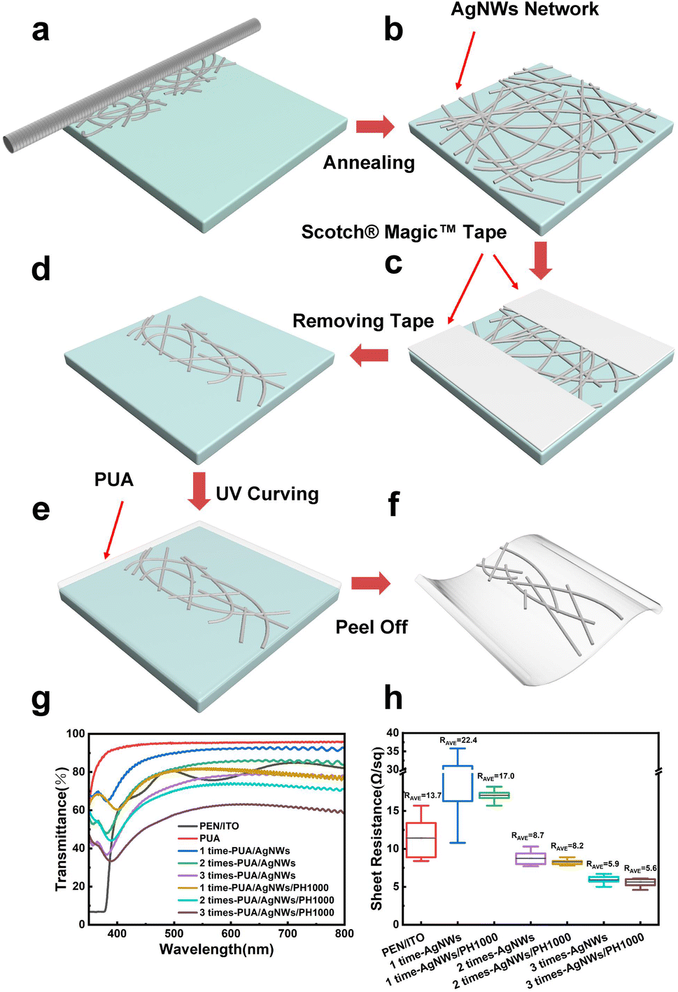 | ||
| Fig. 1 Fabrication and optoelectrical properties of PUA/AgNWs/PH1000 hybrid conductive film. (a–f) Schematic of the fabrication process of PUA/AgNWs/PH1000 hybrid conductive film, (g) the optical transmittance of PUA/AgNWs/PH1000 hybrid conductive film with different bar-coating times, (h) the sheet resistance of PUA/AgNWs/PH1000 hybrid conductive film and the average sheet resistance (RAVE) of different samples are marked. 1 time-AgNWs, 2 times-AgNWs, and 3 times-AgNWs refer to the 1, 2, and 3 bar-coating times of AgNWs, respectively. | ||
The optical transmittance of the hybrid conductive film is shown in Fig. 1g. It's noteworthy that the PUA substrate exhibits a high transmittance over the whole visible wavelength range. At the same time, with the increase of the bar-coating times of AgNWs, the transmittance of PUA/AgNWs decreases obviously, which is attributed to the increased density of AgNWs. After spin-coating PH1000, the transmittance of PUA/AgNWs/PH1000 at 550 nm is 81.4%, 74.0% and 62.4%, respectively, with the bar-coating times extending from one to three. The wave-like characteristics of the transmission spectra are characteristic of the PUA polymer.52
The electrical conductivities of the proposed PUA/AgNWs/PH1000 hybrid conductive film are also compared in Fig. 1h. The resistance and its variation range of the 1 time-AgNW film without PUA and PH1000 are quite large because of the uneven distribution of nanowire conductive channels. When the bar-coating times are increased, the resistance is significantly lowered and the variation range is greatly decreased. After spin-coating PH1000, the resistance variation is further minimized, and the electrode's conductivity exceeds that of the commercial PEN/ITO electrode (13.7 Ω sq−1).
The Figure of Merit (FoM) is a critical parameter for determining the quality of the transparent conductive electrodes, which is defined as the ratio of the electrode's direct current conductivity (σdc) to its optical conductivity (σop):
 | (1) |
As shown in Fig. 2a, the surface morphology of the PUA/AgNWs/PH1000 hybrid conductive film was detected by atomic force microscopy (AFM). The surface roughness of bare AgNWs on the glass substrate is 24.4 nm, and the rough surface will induce a large leakage current, resulting in a dramatically reduced efficiency. After applying PUA to transfer the AgNWs from the glass substrate, the AgNW networks are inlaid onto the surface of PUA, and the morphology is obviously improved. The roughness of PUA/AgNWs is only 1.72 nm (Fig. 2c). After spin-coating PH1000, the surface roughness slightly increases to 1.81 nm (Fig. 2d), which is similar to that of the commercial PEN/ITO flexible conductive film (1.66 nm) (Fig. 2b). Significantly reduced surface roughness will play a positive role in promoting the subsequent device fabrication process by reducing the occurrence of short circuits and improving the quality of active layers. In addition, the AgNWs are thoroughly inlaid in the PUA flexible substrate, resolving the problem of poor adhesion between the nanowires and the traditional substrates.
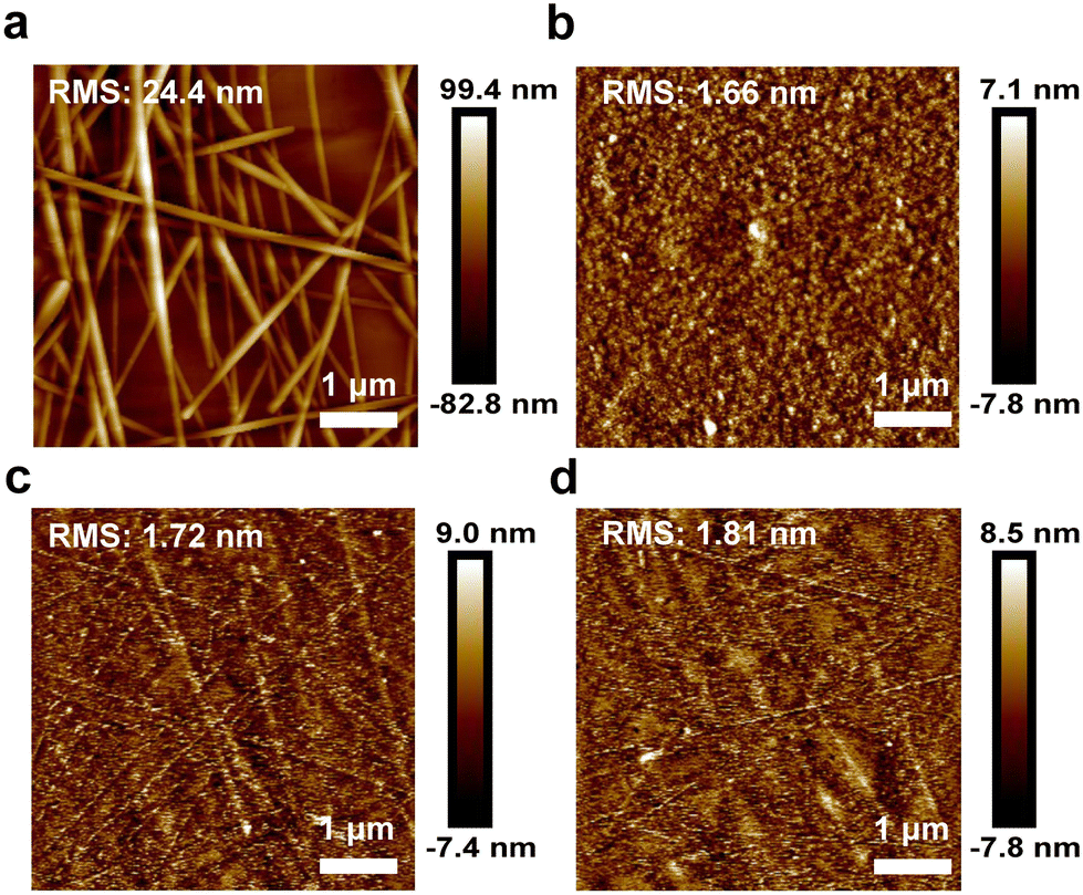 | ||
| Fig. 2 AFM images of (a) glass/AgNWs, (b) PEN/ITO, (c) PUA/AgNWs, and (d) PUA/AgNWs/PH1000. The root-mean-square (RMS) roughness values of the samples are listed. | ||
To explore the potential application of the proposed conductive transparent films in flexible devices, we investigate their mechanical stability by bending test. We measured the resistance under different bending radii (r = ∞, 9, 7, 5 and 3 mm) using a four-probe resistivity tester. The changes of resistances (R/R0, R0 refers to the original resistance without bending, R refers to measured resistance after bending) after 100 bending cycles are shown in Fig. 3a, the PEN/ITO substrates are also used as references. The resistance of PEN/ITO increases dramatically when decreasing the bending radius, which can be attributed to the inherent brittleness of ITO. However, the PUA/AgNW samples demonstrate excellent mechanical stability with the almost unchanged electrical performance, even at a small bending radius of 3 mm.
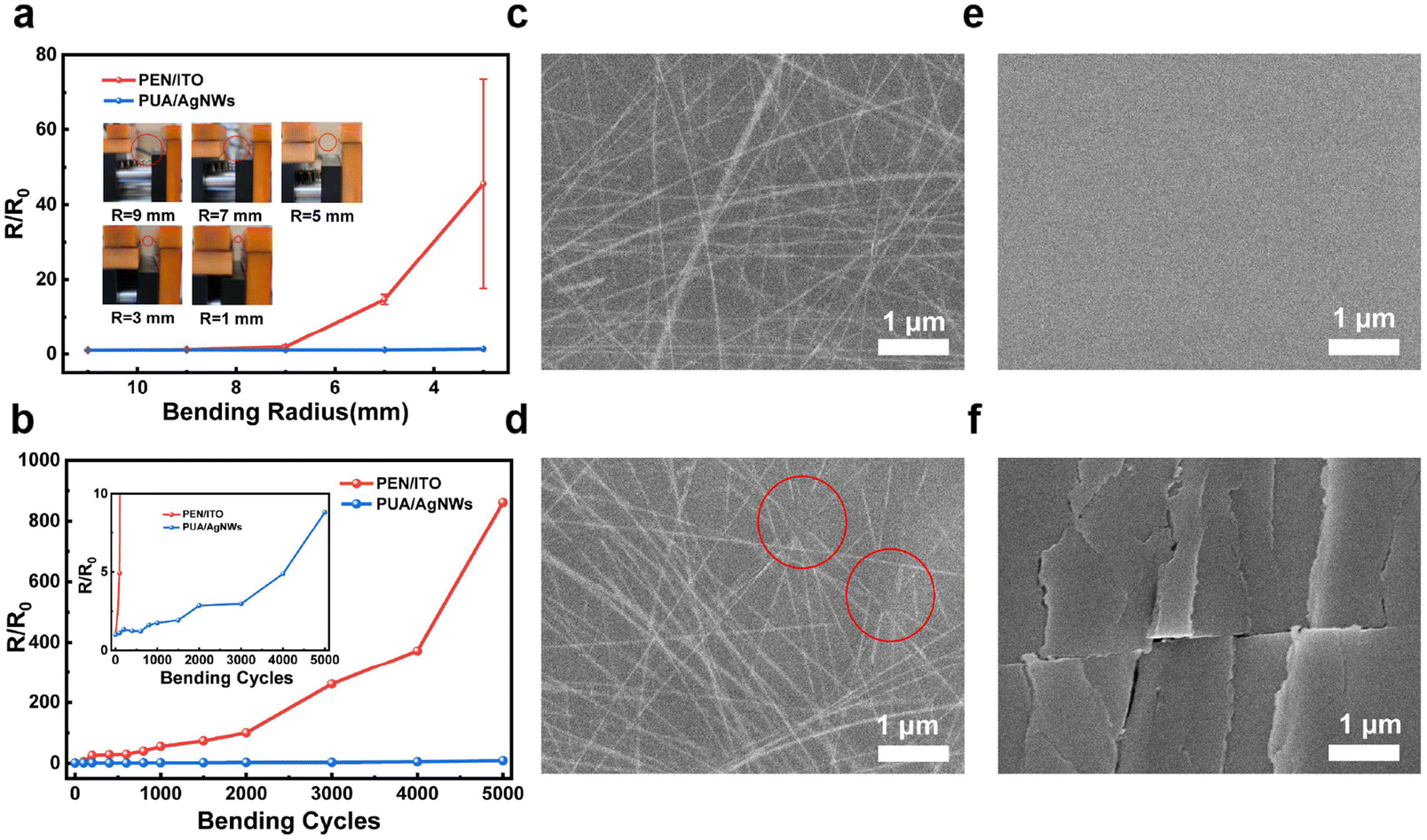 | ||
| Fig. 3 (a) Normalized resistance changes (R/R0) of PEN/ITO and PUA/AgNWs at various bending radius, after 100 bending cycles. The digital images (inset) show the electrodes under bending at different radii (r = ∞, 9 mm, 7 mm, 5 mm and 3 mm). (b) Normalized R/R0 of PEN/ITO and PUA/AgNWs in the function of the bending cycles, at a bending radius of 5 mm. The inset presents zoomed-in values for PEN/ITO and PUA/AgNWs. (c and d) SEM images of PUA/AgNWs before/after bending, at a bending radius of 5 mm. (e and f) SEM images of PEN/ITO before/after bending, at a bending radius of 5 mm. The red cycles mark the broken AgNWs after bending. | ||
We further performed multiple-cycle bending tests with a fixed bending radius of 5 mm. As shown in Fig. 3b, only after 1000 bending cycles, the resistance of PEN/ITO has reached more than 50 times compared with the original level, and further reached more than 850 times of the original resistance after 5000 bending cycles. On the other hand, PUA/AgNWs still maintain high conductivity after 5000 bending cycles, which demonstrates the superior mechanical stability of PUA/AgNWs compared to that of commercial PEN/ITO. In addition, the surface morphologies of different flexible electrodes, before and after repeated bending cycles, have been characterized by scanning electron microscopy (SEM). In Fig. 3c and d, there is no significant change in the surface morphology of PUA/AgNWs before and after bending; only the parts of the AgNWs are broken, which is consistent with a relatively small change in resistance. However, after 3000 bending cycles, PEN/ITO shows significant cracks (Fig. 3e and f) resulting in dramatic decay in conductivity.
For PSCs, electrode morphology has a non-negligible effect on device performances. The crystalline quality of the perovskite polycrystalline film prepared on a smooth and homogeneous substrate can be improved with large perovskite grains, and few grain boundaries and defects, resulting in a high PCE. Fig. 4a and b show the SEM images of the perovskite polycrystalline films prepared on PEN/ITO and PUA/AgNWs/PH1000. The MAPbI3 films show uniform and pinhole-free morphology with the grain sizes ranging from 200 to 400 nm, implying a high crystalline quality on both flexible films. From the X-ray diffraction (XRD) characteristics shown in Fig. 4c, the perovskite films fabricated on PUA/AgNWs/PH1000 further demonstrate similar crystallinity compared to that of the film on PEN/ITO. Both films exhibit two major diffraction peaks with similar intensities at 14.1° and 28.4°, corresponding to the characteristic (110) and (220) diffraction planes of MAPbI3. Fig. 4d shows ultraviolet-visible (UV-vis) absorption spectroscopy of MAPbI3 perovskite films on PUA/AgNWs/PH1000 and PEN/ITO, and the perovskite films on different substrates exhibit an identical absorption profile, implying the similar light absorption capacity.
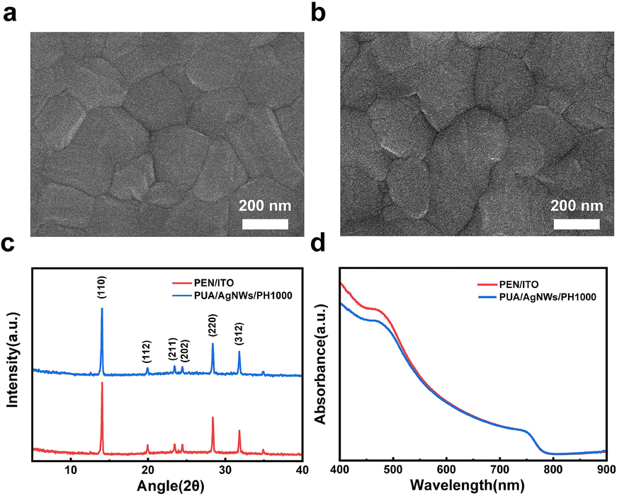 | ||
| Fig. 4 Surface morphology and structure characterization of perovskite films based on PEN/ITO and PUA/AgNWs/PH1000. Top-view SEM images of MAPbI3 films deposited on (a) PEN/ITO and (b) PUA/AgNWs/PH1000. (c) XRD of MAPbI3 films and (d) UV-vis absorption spectrum of the MAPbI3 films on different substrates. | ||
Based on the high transparency, flexibility, and conductivity of the proposed PUA/AgNWs/PH1000 hybrid conductive film, we applied it as a flexible substrate as well as the flexible transparent electrode to fabricate FPSCs with the inverted architecture of PUA/AgNWs/PH1000/PEDOT:PSS/MAPbI3/C60/BCP/Cu (Fig. 5a). The photovoltaic performances are summarized in Fig. 5b and Table S2 in the ESI.† The corresponding forward and reverse current density–voltage (J–V) characteristics are shown in Fig. S1.† The optimal PUA/AgNWs/PH1000 based flexible device realizes an open-circuit voltage (Voc) of 0.867 V, a short-circuit current (Jsc) of 17.05 mA cm−2, and a fill factor (FF) of 74.24%, yielding the best PCE of 10.98% in the reverse scan direction, and realizes a Voc of 0.865 V, Jsc of 16.96 mA cm−2, FF of 72.67%, and PCE of 10.66% in the forward scan direction. For reference, the flexible devices based on PEN/ITO have also been fabricated; the best device achieves a PCE of 12.82%, with Voc of 0.904 V, Jsc of 18.19 mA cm−2, and FF of 77.99%. The PUA/AgNWs/PH1000 based FPSCs exhibit negligible hysteresis, demonstrating the practicality of the PUA/AgNWs/PH1000 hybrid electrode (Table S3 in the ESI†). The differences in Voc and FF between the FPSCs prepared on PUA/AgNWs/PH1000 and PEN/ITO are induced by the different surface properties of electrodes which may lead to the increase of local defects. In addition, comparing to the PEN/ITO-based device, the slightly lowered Jsc should be attributed to the gap in the transmittance between PUA/AgNWs/PH1000 and PEN/ITO as shown in Fig. 1g.
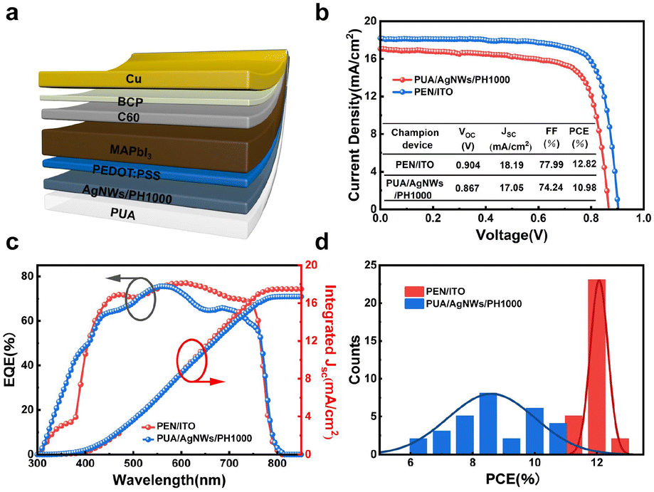 | ||
| Fig. 5 Photovoltaic performance of FPSCs based on PEN/ITO and PUA/AgNWs/PH1000. (a) Schematic illustration of the device architecture. (b) J–V curves of the best devices measured under AM1.5G irradiation with an intensity of 100 mW cm−2. (c) EQE and the corresponding integrated photocurrent curves of FPSCs. (d) Efficiency histogram of FPSCs. | ||
The external quantum efficiency (EQE) of FPSCs based on PUA/AgNWs/PH1000 and PEN/ITO is also provided in Fig. 5c. The integrated currents are 17.50 mA cm−2 and 16.69 mA cm−2, respectively, which perfectly match the current obtained from the J–V curves. To investigate the reproducibility of the devices, the statistical distribution of the PCE based on 30 devices with the PUA/AgNWs/PH1000 and PEN/ITO electrodes is shown in Fig. 5d; the average PCE of the PUA/AgNWs/PH1000-FPSCs is 8.51% ± 2.47%, indicating that the FPSCs based on the PUA/AgNWs/PH1000 hybrid electrodes exhibit relatively good reproducibility. The statistics of the FF, Jsc, Voc, and PCE of PUA/AgNWs/PH1000-FPSCs and PEN/ITO-FPSCs are compared in Fig. S2.† The average efficiency of the PUA/AgNWs/PH1000 based flexible devices is lower than that of the PEN/ITO based flexible devices, because the thick PH1000 inset layer impairs the transmittance of electrodes. On the other hand, to guarantee that the device can operate properly, balanced optical and electrical characteristics are necessary, which further sacrifices the transmittance, resulting in the reduced Jsc and PCE.
The measurement of mechanical stability was applied on FPSCs with a bending radius of 5 mm as shown in Fig. 6a. Due to the inherent brittleness of ITO, it is easily broken during the bending process and the resistance rises sharply; as a result, the efficiency of the device based on PEN/ITO decreases significantly with the increase of bending cycles. The PCE of PEN/ITO-FPSCs has dropped to 14.6% of the initial level after bending 3000 cycles. In contrast, the device based on the PUA/AgNWs/PH1000 maintains 77.4% of the initial efficiency after 10000 bending cycles, which demonstrates the excellent bending stability of PUA/AgNWs/PH1000 and PUA/AgNWs/PH1000-FPSCs and it was among the best bending stability of the reported FPSCs as shown in Table S4 in the ESI.† Furthermore, we performed long-term stability tests of the proposed PUA/AgNWs/PH1000-FPSCs by placing the devices in a N2-filled glove box. As shown in Fig. 6b, after aging for up to 20 days, PUA/AgNWs/PH1000-FPSCs can still retain 69.4% of the initial PCE and exhibit a small gap compared with 85.0% maintenance of the PEN/ITO based device. It should be attributed to the diffusion of the iodide ions from the perovskite active layer to the PUA/AgNWs and the reaction with the AgNWs during the aging process.18 Although we inserted PH1000 on the top of PUA/AgNWs to separate AgNWs from the perovskite active layer, it still could not completely avoid the migration of halogen ions.
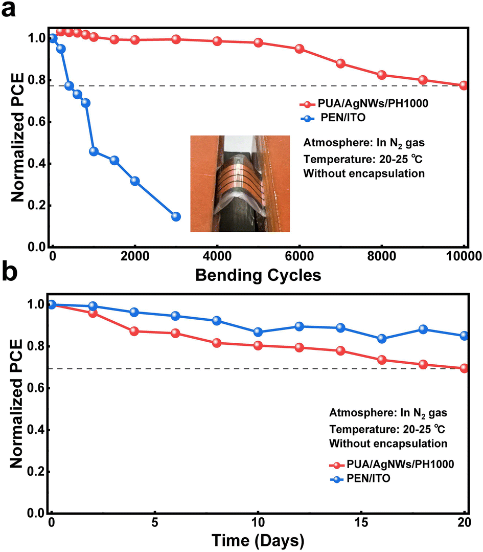 | ||
| Fig. 6 (a) Normalized PCE of the unencapsulated FPSCs as a function of bending cycles with a bending radius of 5 mm. The inset is the photograph of bending FPSCs fabricated on PUA/AgNWs/PH1000. (b) Long-term stability of the devices stored in a N2-filled glove box under dark conditions at room temperature (20–25 °C). | ||
3. Conclusion
In conclusion, FPSCs based on the PUA/AgNWs/PH1000 hybrid transparent electrode are demonstrated for the first time. By embedding AgNWs into PUA, the surface roughness of AgNWs was reduced dramatically from 24.4 nm to 1.72 nm, while resolving the problem of the poor adherence of AgNWs to the substrate. With a PH1000 conductive layer on the top of AgNWs, the metal networks are separated from the perovskite active layer to prevent halogen ions from reacting with AgNWs. The proposed PUA/AgNWs/PH1000 hybrid conductive film with a relatively high optical transmittance (over 70% in the whole visible wavelength range) and a low resistance (8.2 Ω sq−1) acts as an excellent transparent electrode and a flexible substrate in FPSCs, realizing the best PCE of 10.98%. Based on the excellent mechanical stability of PUA/AgNWs/PH1000, the flexibility and bending stability of the PUA/AgNWs/PH1000-FPSCs far exceed those of the devices with the normal PEN/ITO electrode, and they can retain 77.4% of their initial efficiency after 10000 times of bending with a bending radius of 5 mm. The application of the PUA/AgNWs/PH1000 hybrid transparent electrode in FPSCs opens a new way toward wearable photovoltaic devices.
4. Materials and methods
4.1. Materials
Methylammonium iodide (MAI, 99.5%) and lead iodide (PbI2, 99.99%) were purchased from Advanced Election Technology Co., Ltd, and fullerene C60 and 2,9-dimethyl-4,7-diphenyl-1,10-phenanthroline (BCP) were obtained from Luminescence Technology Co. The anhydrous solvents N,N-dimethylformamide (DMF, 99.8%), dimethyl sulfoxide (DMSO, 99.9%), ethyl acetate (EA, 99.8%) and 2-hydroxy-2-methylpropiophenone (97%) were purchased from Sigma-Aldrich. Poly(3,4-ethylenedioxythiophene)-poly(styrene sulfonate) (PEDOT:PSS, Cleviost™ PH1000 and Cleviost™ PVP AI 4083) was purchased from Heraeus (Germany). Zonyl FS-300 was purchased from DuPont. Silver nanowires (AgNWs) (average diameter = 25–35 nm; average length = 10–40 μm) were obtained from Zhejiang Kechuang Advanced Materials Co. UA (CN990) and EBA (SR540) were purchased from Sartomer. All materials were received and used without any purification.4.2. Preparation of PUA solution
The siliconized urethane acrylate oligomer (UA, CN990), dimethacrylate (EBA, SR540), and 2-hydroxy-2-methylpropiophenone were mixed at a weight ratio of 10:2:1. After adequate shaking, the mixture was sonicated for more than 24 hours before use.
4.3. Fabrication of PUA/AgNW hybrid electrodes
The AgNW network film was prepared by repeatedly bar coating the AgNW suspension solution (4.5 mg ml−1 in isopropanol) with a Mayer rod (No. 8) on glass substrates. The AgNW films were annealed at 150 °C for 10 min. After cooling down to room temperature, Scotch® Magic™ Tapes were used to etch out the electrode pattern. Then, PUA solution was spin-coated onto the substrate at 2000 rpm for 60 s. The prepared sample was subjected to UV light exposure for 10 min and then the PUA/AgNW hybrid film was carefully peeled off from the glass substrate. PDMS solution was obtained by mixing the silicone elastomer base, curing agent, and hexane at a weight ratio of 10:1:5; the supernatant was spin-coated onto the pre-cleaned glass substrates at 5000 rpm for 30 s after stirring and degassing, and subsequently annealed at 150 °C for 10 min. After that, the PUA/AgNW film was adhered to the PDMS/glass temporary substrates to keep the surface flat. Note that after the fabrication of the perovskite solar cells, the PDMS/glass temporary substrate was removed to realize flexible devices. Finally, the PUA/AgNWs/PH1000 hybrid electrodes were obtained by spin-coating PEDOT:PSS (PH1000, Cleviost™) mixed with 5 wt% DMSO at 3000 rpm for 30 s and then annealing at 100 °C for 15 min. To guarantee the desired pattern of the conductive electrode, we used Scotch® Magic™ Tapes to cover the non-electrode part before spin-coating PEDOT:PSS (PH1000), and removed the tapes before the annealing process.
4.4. Fabrication of FPSCs
The prepared PUA/AgNWs/PH1000 hybrid conductive films were plasma treated for 5 min. Zonyl FS-300 with a concentration of 1.0 wt% was added into the PEDOT:PSS (AI 4083, Cleviost™) solution and the mixture solutions were stirred overnight before use. The Zonyl-doped PEDOT:PSS (AI 4083) solution was spin-coated at 4000 rpm for 40 s on prepared electrodes and annealed at 100 °C for 15 min. Then, the samples were transferred to a N2-filled glovebox. The perovskite precursor was obtained by mixing MAI (1.3 mmol) and PbI2 (1.3 mmol) in 1 mL of the DMF and DMSO mixture (4:1 v/v). The precursor was spin-coated onto the PEDOT:PSS layer at 1000 rpm for 3 s and 4000 rpm for 30 s consecutively. The anti-solvent of EA was dropped onto the samples consecutively in the last 10 s of the spin-coating process. The perovskite film was annealed at 50 °C for 5 min and then 100 °C for 30 min. After the samples cooled down to room temperature, 25 nm C60, 7 nm BCP (Bathocuproine), and 100 nm Cu electrode were thermally deposited onto the perovskite film at a rate of 0.3, 0.2 and 1.0 Å s−1, respectively. The device area of FPSCs was 4 mm2.
4.5. Characterization
The J–V performances of the PSCs were measured using a Keithley 2400 source meter. The J–V hysteresis curves were obtained by the forward (from −0.2 V to 1.2 V) and reverse scans (from 1.2 V to −0.2 V) with a scan rate of 100 mV s−1, under AM1.5G irradiation based on a AAA grade solar simulator (XES-70S1, SAN-EI Electric co., Ltd) in a N2-filled glovebox. A standard Si solar cell equipped with a KG-5 filter was applied to calibrate the light intensity (100 mW cm−2). The EQE was detected via a QE-R3011 system (Enli Technology co., Ltd). The roughness of the perovskite surface morphology was measured by AFM (Dimension Icon, Bruker). The UV-vis absorption spectra were measured using a UV-visible diffuse reflectance spectrophotometer (Hatachi U3900H). The surface profile of the perovskite was characterized using a SEM (JSM-7900F). XRD measurement was obtained using a Rigaku D/max 2550 X-ray diffractometer with a monochromatized Cu target radiation source.Conflicts of interest
There are no conflicts to declare.Acknowledgements
This work was supported by the National Key Research and Development Program of China (2020YFA0715000), the National Natural Science Foundation of China (61825402), the Natural Science Foundation of Chongqing (CSTB2022NSCQ-MSX1155), and the Interdisciplinary Integration and Innovation Project of Jilin University (JLUXKJC2020318).References
- A. Kojima, K. Teshima, Y. Shirai and T. Miyasaka, J. Am. Chem. Soc., 2009, 131, 6050–6051 CrossRef CAS PubMed.
- Z. Wang, Y. Han, L. Yan, C. Gong, J. Kang, H. Zhang, X. Sun, L. Zhang, J. Lin, Q. Luo and C.-Q. Ma, Adv. Funct. Mater., 2021, 31, 2007276 CrossRef CAS.
- K. Yao, S. Li, Z. Liu, Y. Ying, P. Dvorak, L. Fei, T. Sikola, H. Huang, P. Nordlander, A. K. Y. Jen and D. Lei, Light: Sci. Appl., 2021, 10, 219 CrossRef CAS PubMed.
- S. B. Kang, J.-H. Kim, M. H. Jeong, A. Sanger, C. U. Kim, C.-M. Kim and K. J. Choi, Light: Sci. Appl., 2019, 8, 121 CrossRef CAS PubMed.
- Z. Ren, K. Liu, H. Hu, X. Guo, Y. Gao, P. W. K. Fong, Q. Liang, H. Tang, J. Huang, H. Zhang, M. Qin, L. Cui, H. T. Chandran, D. Shen, M.-F. Lo, A. Ng, C. Surya, M. Shao, C.-S. Lee, X. Lu, F. Laquai, Y. Zhu and G. Li, Light: Sci. Appl., 2021, 10, 239 CrossRef CAS PubMed.
- D. Yin, N.-R. Jiang, Y.-F. Liu, X.-L. Zhang, A.-W. Li, J. Feng and H.-B. Sun, Light: Sci. Appl., 2018, 7, 35 CrossRef PubMed.
- Y. Jeon, H.-R. Choi, J. H. Kwon, S. Choi, K. M. Nam, K.-C. Park and K. C. Choi, Light: Sci. Appl., 2019, 8, 114 CrossRef CAS PubMed.
- L. Li, Z. Yu, W. Hu, C.-H. Chang, Q. Chen and Q. Pei, Adv. Mater., 2011, 23, 5563–5567 CrossRef CAS PubMed.
- R. Sun, D. Zhou, Y. Ding, Y. Wang, Y. Wang, X. Zhuang, S. Liu, N. Ding, T. Wang, W. Xu and H. Song, Light: Sci. Appl., 2022, 11, 340–340 CrossRef CAS PubMed.
- M. Amjadi, A. Pichitpajongkit, S. Lee, S. Ryu and I. Park, ACS Nano, 2014, 8, 5154–5163 CrossRef CAS PubMed.
- W. Deng, X. Zhang, L. Huang, X. Xu, L. Wang, J. Wang, Q. Shang, S.-T. Lee and J. Jie, Adv. Mater., 2016, 28, 2201–2208 CrossRef CAS PubMed.
- A. Ciavatti, R. Sorrentino, L. Basirico, B. Passarella, M. Caironi, A. Petrozza and B. Fraboni, Adv. Funct. Mater., 2021, 31, 2009072 CrossRef CAS.
- M. Naqi, B. Kim, S.-W. Kim and S. Kim, Adv. Funct. Mater., 2021, 31, 2007389 CrossRef CAS.
- T. Su, N. Liu, D. Lei, L. Wang, Z. Ren, Q. Zhang, J. Su, Z. Zhang and Y. Gao, ACS Nano, 2022, 16(2), 8461–8471 CrossRef CAS PubMed.
- C. Xie, P. You, Z. Liu, L. Li and F. Yan, Light: Sci. Appl., 2017, 6, e17023 CrossRef PubMed.
- S. A. Hashemi, S. Ramakrishna and A. G. Aberle, Energy Environ. Sci., 2020, 13, 685–743 RSC.
- L. Yang, J. Feng, Z. Liu, Y. Duan, S. Zhan, S. Yang, K. He, Y. Li, Y. Zhou, N. Yuan, J. Ding and S. F. Liu, Adv. Mater., 2022, 34, 2201681 CrossRef CAS PubMed.
- J. Wang, X. Chen, F. Jiang, Q. Luo, L. Zhang, M. Tan, M. Xie, Y.-Q. Li, Y. Zhou, W. Su, Y. Li and C.-Q. Ma, Sol. RRL, 2018, 2, 1800118 CrossRef.
- M. Park, H. J. Kim, I. Jeong, J. Lee, H. Lee, H. J. Son, D.-E. Kim and M. J. Ko, Adv. Energy Mater., 2015, 5, 1501406 CrossRef.
- K.-W. Seo, J. Lee, J. Jo, C. Cho and J.-Y. Lee, Adv. Mater., 2019, 31, 1902447 CrossRef PubMed.
- B. J. Kim, D. H. Kim, Y.-Y. Lee, H.-W. Shin, G. S. Han, J. S. Hong, K. Mahmood, T. K. Ahn, Y.-C. Joo, K. S. Hong, N.-G. Park, S. Lee and H. S. Jung, Energy Environ. Sci., 2015, 8, 916–921 RSC.
- N.-R. Jiang, Y.-F. Wang, Q.-F. Dong, C.-D. Ge, Z.-Q. Yang, D. Yin, Y.-F. Liu, Y.-G. Bi, J. Feng and H.-B. Sun, Sol. RRL, 2021, 5, 2000821 CrossRef CAS.
- J. Zhou, S. Li, X. Lv, X. Li, Y. Li, Y.-Z. Zheng and X. Tao, J. Power Sources, 2020, 478, 228764 CrossRef CAS.
- F. L. M. Sam, C. A. Mills, L. J. Rozanski and S. R. P. Silva, Laser Photonics Rev., 2014, 8, 172–179 CrossRef CAS.
- W. Deng, F. Li, J. Li, M. Wang, Y. Hu and M. Liu, Nano Energy, 2020, 70, 104505 CrossRef CAS.
- S. Ye, A. R. Rathmell, Z. Chen, I. E. Stewart and B. J. Wiley, Adv. Mater., 2014, 26, 6670–6687 CrossRef CAS PubMed.
- J. Yoon, U. Kim, Y. Yoo, J. Byeon, S.-K. Lee, J.-S. Nam, K. Kim, Q. Zhang, E. I. Kauppinen, S. Maruyama, P. Lee and I. Jeon, Adv. Sci., 2021, 8, 2004092 CrossRef CAS PubMed.
- I. Jeon, J. Yoon, U. Kim, C. Lee, R. Xiang, A. Shawky, J. Xi, J. Byeon, H. M. Lee, M. Choi, S. Maruyama and Y. Matsuo, Adv. Energy Mater., 2019, 9, 1901204 CrossRef.
- J. H. Heo, D. H. Shin, S. Kim, M. H. Jang, M. H. Lee, S. W. Seo, S.-H. Choi and S. H. Im, Chem. Eng. J., 2017, 323, 153–159 CrossRef CAS.
- J. H. Heo, D. H. Shin, D. H. Song, D. H. Kim, S. J. Lee and S. H. Im, J. Mater. Chem. A, 2018, 6, 8251–8258 RSC.
- Z. Yin, S. Sun, T. Salim, S. Wu, X. Huang, Q. He, Y. M. Lam and H. Zhang, ACS Nano, 2010, 4, 5263–5268 CrossRef CAS PubMed.
- Z. Jin, J. Yan, X. Huang, W. Xu, S. Yang, D. Zhu and J. Wang, Nano Energy, 2017, 40, 376–381 CrossRef CAS.
- M. Vosgueritchian, D. J. Lipomi and Z. Bao, Adv. Funct. Mater., 2012, 22, 421–428 CrossRef CAS.
- M. Li, W.-W. Zuo, A. G. Ricciardulli, Y.-G. Yang, Y.-H. Liu, Q. Wang, K.-L. Wang, G.-X. Li, M. Saliba, D. Di Girolamo, A. Abate and Z.-K. Wang, Adv. Mater., 2020, 32, 2003422 CrossRef CAS PubMed.
- Y. W. Li, L. Meng, Y. Yang, G. Y. Xu, Z. R. Hong, Q. Chen, J. B. You, G. Li, Y. Yang and Y. F. Li, Nat. Commun., 2016, 7, 10214 CrossRef CAS PubMed.
- Y.-F. Li, S.-Y. Chou, P. Huang, C. Xiao, X. Liu, Y. Xie, F. Zhao, Y. Huang, J. Feng, H. Zhong, H.-B. Sun and Q. Pei, Adv. Mater., 2019, 31, 1807516 CrossRef PubMed.
- P. Ma, Y. Lou, S. Cong, Z. Lu, K. Zhu, J. Zhao and G. Zou, Adv. Energy Mater., 2020, 10, 1903357 CrossRef CAS.
- Z. Lu, Y. Lou, P. Ma, K. Zhu, S. Cong, C. Wang, X. Su and G. Zou, Sol. RRL, 2020, 4, 2000320 CrossRef CAS.
- J.-Y. Tseng, L. Lee, Y.-C. Huang, J.-H. Chang, T.-Y. Su, Y.-C. Shih, H.-W. Lin and Y.-L. Chueh, Small, 2018, 14, 1800541 CrossRef PubMed.
- M.-R. Azani and A. Hassanpour, Chem. – Eur. J., 2018, 24, 19195–19199 CrossRef CAS PubMed.
- J. Ahn, H. Hwang, S. Jeong and J. Moon, Adv. Energy Mater., 2017, 7, 1602751 CrossRef.
- E. Lee, J. Ahn, H.-C. Kwon, S. Ma, K. Kim, S. Yun and J. Moon, Adv. Energy Mater., 2018, 8, 1702182 CrossRef.
- N. H. Khoa, Y. Tanaka, W. P. Goh and C. Y. Jiang, Sol. Energy, 2020, 196, 582–588 CrossRef CAS.
- S. Y. Lee, Y. S. Nam, J. C. Yu, S. Lee, E. D. Jung, S.-H. Kim, S. Lee, J.-Y. Kim and M. H. Song, ACS Appl. Mater. Interfaces, 2019, 11, 39274–39282 CrossRef CAS PubMed.
- H. Lee, D. Lee, Y. Ahn, E.-W. Lee, L. S. Park and Y. Lee, Nanoscale, 2014, 6, 8565–8570 RSC.
- J. A. Spechler, T.-W. Koh, J. T. Herb, B. P. Rand and C. B. Arnold, Adv. Funct. Mater., 2015, 25, 7428–7434 CrossRef.
- H. Lu, J. Sun, H. Zhang, S. Lu and W. C. H. Choy, Nanoscale, 2016, 8, 5946–5953 RSC.
- Y. Liu, J. Zhang, H. Gao, Y. Wang, Q. Liu, S. Huang, C. F. Guo and Z. Ren, Nano Lett., 2017, 17, 1090–1096 CrossRef CAS PubMed.
- M.-R. Azani, A. Hassanpour and T. Torres, Adv. Energy Mater., 2020, 10, 2002536 CrossRef CAS.
- T.-Y. Jin, W. Li, Y.-Q. Li, Y.-X. Luo, Y. Shen, L.-P. Cheng and J.-X. Tang, Adv. Opt. Mater., 2018, 6, 1801153 CrossRef.
- J. Liang, L. Li, X. Niu, Z. Yu and Q. Pei, Nat. Photonics, 2013, 7, 817–824 CrossRef CAS.
- D. Chen, J. Liang, C. Liu, G. Saldanha, F. Zhao, K. Tong, J. Liu and Q. Pei, Adv. Funct. Mater., 2015, 25, 7512–7520 CrossRef.
- Y. H. Kim, C. Sachse, M. L. Machala, C. May, L. Mueller-Meskamp and K. Leo, Adv. Funct. Mater., 2011, 21, 1076–1081 CrossRef CAS.
- National Renewable Energy Laboratory, Best research-cell efficiencies chart, https://www.nrel.gov/pv/cell-efficiency.html.
Footnote |
| † Electronic supplementary information (ESI) available. See DOI: https://doi.org/10.1039/d2nr07026j |
| This journal is © The Royal Society of Chemistry 2023 |