
Revealing the effect of substitutional cation doping in the A-site of nanoscale APbI3 perovskite layers for enhanced retention and endurance in optoelectronic resistive switching for non-volatile bipolar memory devices†
Twinkle
George
and
Arumugam
Vadivel Murugan
 *
*
Advanced Functional Nanomaterials Research Laboratory, Centre for Nanoscience and Technology, Madanjeet School of Green Energy Technologies, Pondicherry University (A Central University), Dr. R. Vankataraman Nagar, Kalapet, Puducherry-605014, India. E-mail: avmrajeshwar@gmail.com; avmurugan.nst@pondiuni.edu.in
First published on 20th March 2023
Abstract
The effect of substitutional cation doping in the A-site of the nanoscale APbI3 perovskite layer has been systematically investigated to achieve improvements in the charge-carrier dynamics and endurance of non-volatile bipolar (NVB) memory devices. We successfully adopted an energy-efficient, ultra-fast microwave-assisted solvothermal (MW-ST) synthesis route to prepare a sequence of APbI3 (A = MA+, FA+, MAFA+, CsMA+ and CsMAFA+) perovskite powders with morphological transitions from cube-like polyhedrons to mixed polyhedrons and rods within 10 minutes at 120 °C without requiring any inert-gas atmosphere under high-humid ambient conditions. As-prepared APbI3 powders were dissolved in DMSO:DMF, followed by the fabrication of a thin film via spin-coating. Upon annealing at 120 °C, the nanoscale self-assembled thin-film layer was formed. We observed that devices with the inorganic Cs+ cation with organic cations, (CsMAPI and CsMAFAPI) device showed improved endurance (3500 and 5000 cycles, respectively) and outstanding retention (60![[thin space (1/6-em)]](https://www.rsc.org/images/entities/char_2009.gif) 000 s) owing to effective charge-carrier dynamics, compared to organic cation-based MAPI, FAPI and MAFAPI (1800, 1200 and 1300 cycles, respectively). Significantly, various cation-doped APbI3-powders obtained via the MW-ST method remained to be stable for up to 5-months under high-humid conditions. Thus, enhanced optoelectronic-memory performance studies could provide an opportunity for next-generation nanoscale ORSNVB-memory devices for artificial intelligence (AI) and Internet of Things (IoT) applications.
000 s) owing to effective charge-carrier dynamics, compared to organic cation-based MAPI, FAPI and MAFAPI (1800, 1200 and 1300 cycles, respectively). Significantly, various cation-doped APbI3-powders obtained via the MW-ST method remained to be stable for up to 5-months under high-humid conditions. Thus, enhanced optoelectronic-memory performance studies could provide an opportunity for next-generation nanoscale ORSNVB-memory devices for artificial intelligence (AI) and Internet of Things (IoT) applications.
Introduction
Nanoscale-memristors, identified as a fundamental active electronic component, can operate at low voltage and high storage density with simple architecture for the development of next-generation optoelectronic resistive switching non-volatile bipolar (ORSNVB) memory devices, and have attracted significant attention for their application in artificial intelligence (AI), artificial vision (AV), and photonic memory (PM) systems.1–3 In this regard, semiconducting inorganic metal oxides with perovskite structure, two-dimensional chalcogenides, and inorganic and organic functional materials are extensively studied as active materials for ultra-thin ORSNVB memory devices.4,5 However, the fabrication of these oxide-based devices requires extremely sophisticated physical processing techniques, complex synthesis routes, and high-temperature annealing, thereby hampering their practical applications.5 Hence, it is necessary to develop multi-functional optoelectronic materials that could be processed via facile low-cost solution-process techniques and could offer superior switching performance for a viable ORSNVB memory device.Recently, metal halide perovskites (MHPs), such as CH3NH3PbI3, CH(NH2)2PbI3, CsPbI3, CsPbBr3, and Cs4PbBr6, have emerged as the most promising semiconductors for a broad range of optoelectronic devices, including LEDs, photovoltaics, transistors, and memristors6–9 as they possess desirable features such as long diffusion path-lengths, high carrier mobility, ambipolar charge-transport, high carrier lifetime, low trap-density, efficient photoelectric-conversion, and low processing feasibility in terms of cost and energy.8–11 Additionally, they promote flexible thin-film devices, making them compatible with the roll-to-roll (R2R) process for mass production.11,12 Among MHPs, nanolayered organic–inorganic CH3NH3PbI3 (MAPI) perovskite-structured material possesses remarkable optoelectronic functionalities, which are suitable for bipolar resistive switching memory devices. However, they have drawbacks such as chemical and structural instability with an adverse reaction to atmospheric moisture.12,13 To overcome these limitations, significant efforts have been made by chemical compositional tuning via cation or anion exchange, and doping of perovskite material by adopting suitable methodologies. Indeed, altering the cations to find a substitute for the ‘A’-site cation is particularly desirable, as the ionic size of the ‘A’-site cation stabilizes the ABX3 perovskite structure. Moreover, the interaction of the ‘A’-site cation with the inorganic lattice modifies the optoelectronic device functionalities.14,15
Doping of formamidinium [FA+, CH(NH2)2+], cesium (Cs+), and mixed cations such as methyl ammonium/formamidinium [(MA+/MAFA+) (CH3NH3+/CH(NH2)2+)], CsMA+, and CSMAFA+ into the A-site of APbI3 lattice in the place of MA+ is feasible as they have ionic radii comparable to that of the MA+ cation. Additionally, the incorporation of FA+, Cs+ ions, and their mixed cations (MAFA+, CsMA+, and CsMAFA+) in the APbI3 lattice leads to significant optoelectronic properties, improved structural and chemical stability and can affect the light/electric field-induced ionic migration for the improved device performance.16,17 However, effective cation doping into the APbI3 lattice is still a challenge, and systematic investigations related to the effect of doping on the charge transport properties, crystallinity, and morphology of APbI3 perovskite structure in correlation with ORSNVB performance are inadequate. Several studies on the synthesis of cation doping in APbI3 perovskites have been conducted, which include the solution process, coprecipitation, chemical vapour deposition, and solvothermal (ST) method.18,19 Among them, ST is advantageous for controlling the morphology, crystal size, shape, and homogeneity. However, they require long duration and complex synthesis procedures. In this regard, combining microwave reaction chemistry under solvothermal condition (MW-ST) is an advanced sustainable technology. Microwave irradiation in the polar solvents can initiate dipole–dipole interactions of the solvent-molecules, which can accelerate the reaction rates and provide rapid and uniform heating, thus generating autogenous pressure within the reaction vessel. It also offers improved product yield with high-pure material and the obtained products are chemically stable. In heterogeneous solid–liquid reaction conditions, the speedy input of high-frequency electromagnetic energy sources creates many ‘hot spots’ in the reaction vessel consequently favouring rapid nucleation and prompt crystallization.20 For more than a decade, our research group has effectively adopted the microwave-assisted hydrothermal/solvothermal (MW-HT/ST) technique to prepare various advanced functional materials within a few minutes.20–23
In the present study, we successfully demonstrate the effective doping of various inorganic and organic cations in the A-site of APbI3 (A = MA+, FA+, MAFA+, CsMA+, and CsMAFA+) perovskite structure to form methylammonium lead iodide (MAPI), formamidinium lead iodide (FAPI), methyl ammonium formamidinium lead iodide (MAFAPI), cesium methylammonium lead iodide (CsMAPI) and cesium methylammonium formamidinium lead iodide (CsMAFAPI) powders using an energy-efficient and ultra-fast MW-ST method within 10 minutes at 120 °C without requiring any inert-gas atmosphere. The as-synthesized MHP powders were dissolved in aprotic solvents, DMF:DMSO (8:2) and subsequently, were allowed to recrystallize via the solution-based nanoscale self-assembled process into a thin film using the facile and cost-effective spin-coating technique, upon annealing at 120 °C. A series of ORSNVB devices were fabricated and the cation-induced effects on structure, morphology, and optoelectronic resistive switching memory performances are systematically investigated. Correspondingly, the Ag/CsMAFAPI/FTO configured ORSNVB memory device exhibited remarkable photonic memory application under high-humid ambient conditions (Pondicherry, India, 65 ± 5% RH, and ∼28 °C).
Results and discussion
APbI3 metal halide perovskites (MHPs) possess an ABX3 structure, which allows predominant flexibility for compositional design. Herein, the PbI6− framework contributes extensively towards the anionic framework while the A-site cation occupies the cubical cavity formed by the anionic octahedral cage.24 Indeed, X− halides contribute majorly towards the bandgap of the perovskite material, while the A-site cation plays a significant role in stabilizing the perovskite structure. The variation in cationic radii can directly affect the tilting of the PbI6 cage and distorts the I–Pb–I bond lengths and bond angles influencing the photophysical properties in addition to the perovskite structure.24–27 Interestingly, the interaction of the A-site cation with the PbI6 octahedral cage can be determined by the Goldschmidt tolerance factor (t), which is estimated using the ionic radii of the A-site cation. In this regard, a tolerance factor of 0.8 < 1.1 is required to form a stable perovskite structure that would enable improved optoelectronic properties. After doping with various cations the ionic radii of the MA+, FA+, and Cs+ cations became 217, 253, and 167 pm, respectively,25 and the ionic radii for the mixed cations substituted in the A-site such as MAFA+, CsMA+, and CsMAFA+ were estimated as 235, 192, 191.1 pm, respectively. The tolerance factor for the various cations doped samples is found to be lying between 0.8 to 1.1, which clearly indicates the formation of stable perovskite structure with improved optoelectronic properties. The calculated tolerance factor (t) was observed to be low for the mixed cation-based CsMAFAPI and CsMAPI, followed by MAPI, while the highest t has been observed for MAFAPI and FAPI. The overall order of the tolerance factor for the series of APbI3 metal halide perovskites synthesized via the microwave-solvothermal (MW-ST) method is FAPI > MAFAPI > MAPI > CsMAPI > CsMAFAPI. Tables S1 and S2† show consolidated tolerance factors (t) for the various cation-doped APbI3 metal halide perovskites that were synthesized via the microwave-assisted solvothermal (MW-ST) method.X-ray diffraction studies
Fig. 1a shows the XRD pattern of the various cation-doped MW-ST APbI3 (A = MA+, FA+, MAFA+, CsMA+, and CsMAFA+) perovskite powders synthesized via the MW-ST method. The observed pattern can be indexed to the tetragonal phase (I4cm space group, PDF no. 98-011-4280). The sharp diffraction peaks, located at 2θ = 14, 20, 24.5, 28.4, and 31.9° angles, corresponding to the (001), (011), (111), (002), and (012), respectively, diffraction planes indicate highly crystalline nature of the obtained samples.28 It is interesting to observe that no peaks related to the monohydrate secondary phase of lead iodide were identified in the obtained XRD pattern. However, peaks belonging to the non-perovskite δ-phase of FAPI were obtained at 2θ = 12.7, 25.95, and 34.3° angles when the A-site was substituted with the FA+ cation, corroborating the large tolerance factor (t).29 Additionally, the peaks were slightly shifted towards lower angles indicating the intercalation of the larger ionic radius of the FA+ cations [r = 0.25 nm]. In contrast, the peaks shift towards higher angles in the case of dopants with smaller ionic radii such as Cs+ (r = 0.17 nm) when compared to the MA+ cation (r = 0.22 nm).30 Indeed, the enhanced peak intensities clearly depict the formation of high-crystalline MHP with the incorporation of cations such as MA+, MAFA+, CsMA+, and CsMAFA+ into the A-site of the APbI3 metal halide perovskite lattice. Fig. 1c shows the shift of 2θ to lower angles further confirming the variation of lattice constants and the corresponding incorporation of cations into the perovskite lattice.31 The enlarged peaks of the as-synthesized APbI3 perovskite at 2θ = 14° is shown in Fig. S1.† Moreover, the splitting of planes (004) and (220) observed at 28° and 32°, respectively, represents the formation of a tetragonal perovskite structure, further confirming the cation doping into the A-site of the APbI3 perovskite structure. During the MW-ST synthesis process, providing enough time (10 min holding) and pressure to reach the supercritical state beyond the boiling point of the precursor mixture at elevated temperature favours this crystallinity of the various cation-doped APbI3 perovskite formation.32 Table S3† summarizes the detailed XRD pattern with lattice parameters for the APbI3, which was obtained via the MW-ST method. The XRD results further confirm the role of crystallinity and cationic radii of the cation in the A-site for stabilizing the APbI3 structure, which can contribute to improving the device performance.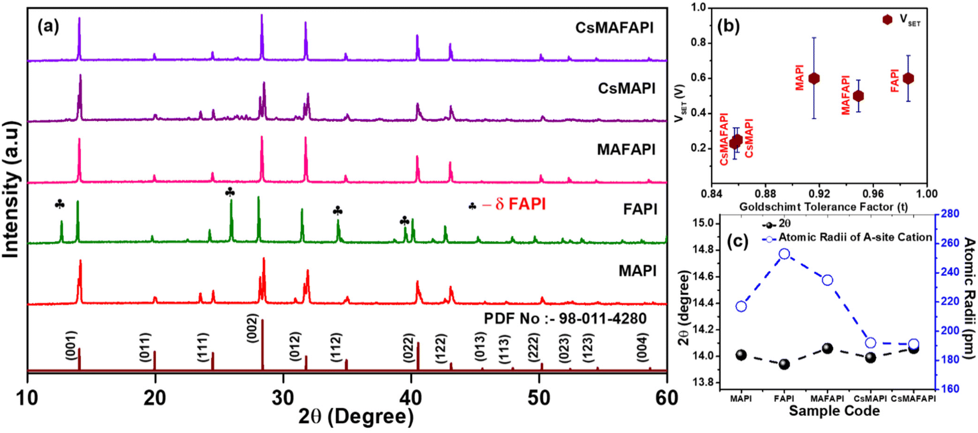 | ||
| Fig. 1 (a) XRD pattern of the MW-ST synthesized APbI3 (A = MA+, FA+, MAFA+, CsMA+ and CsMAFA+) metal halide perovskite powders depicting the (b) variation of Goldschmidt tolerance factor with the operation VSET voltage and (c) the shift of 2θ = 14°, with respect to the atomic radii of the substitutional cations. | ||
Resistive switching memory performance
The effect of the substitutional doping of cations possessing different ionic radii in the A-site of APbI3 metal halide perovskites (MHP) on the resistive switching performance was studied by fabricating the devices with the configuration Ag/APbI3/FTO, where A = MA+, FA+, CsMA+, and CsMAFA+. Gradual heating at 5 °C min−1 was provided to allow 1 mM of pre-synthesized APbI3 perovskite powders to dissolve in DMF:DMSO to recrystallize into a nanoscale thin film on the bottom of the FTO substrates. The nanoscale thin films were allowed to anneal at 120 °C for 10 minutes to complete the crystallization. Further, the films were allowed to cool down to room temperature gradually, to obtain, homogeneous and smooth perovskite films.To reveal the memory performance, characterisation of the fabricated APbI3 memory devices by semi-logarithmic current–voltage (I–V) was studied under ambient conditions with a steady DC supply of ±5 V to enable the traps, that facilitated the formation of conductive channels or conductive filaments (CFs). In order, to prevent the premature breakdown of the conduction filaments (CFs), a compliance current (CC) was set at 1 mA.33Fig. 2a illustrates the schematic depiction of the fabricated optoelectronic resistive switching non-volatile bipolar (ORSNVB) memory device with Ag/APbI3/FTO configuration. We observed that when the applied voltage was swept between 5 V and −5 V, regardless of the cation substituted in the A-site of the APbI3, the devices exhibited resistive switching in both directions, which clearly indicated a bipolar resistive switching behaviour of the device. During the sweep of positive voltage, the current exponentially rises denoting the formation of conductive filaments (CFs), which enables the low resistance state (LRS). The voltage value at which the current overshoots can be denoted as the state of being “ON” or with a digital equivalence of “1”, known as the process of SET. On the other hand, during the negative sweep, we observed a rather gradual leap down of current denoting the RESET process due to the dissociation of CFs creating a high resistance state (HRS).34,35
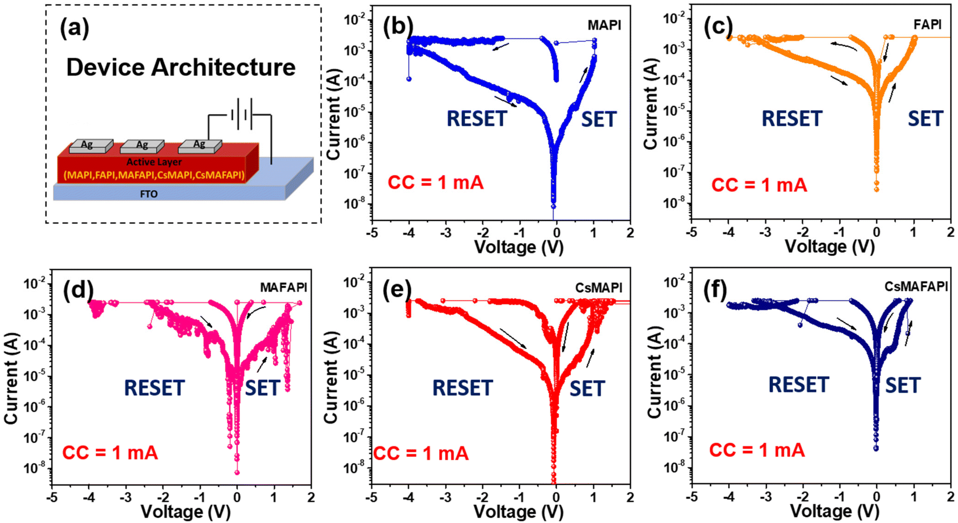 | ||
| Fig. 2 (a) Schematic illustration of the Ag/APbI3/Ag memory device with facile sandwich architecture. The semi-logarithmic resistive switching performance for (b) Ag/MAPI/FTO (c) Ag/FAPI/FTO (d) Ag/MAFAPI/FTO, (e) Ag/CsMAPI/FTO and (f) Ag/CsMAFAPI/FTO memory devices. | ||
Fig. 2b–f clearly isolates the effect of the A-site cation on the device performance and shows the semi-logarithmic I–V curves for the ORSNVB memory devices. Interestingly, we perceived that the trends in operating voltage (VSET) of the semi-logarithmic I–V characteristics are strongly influenced by the estimated Goldschmidt tolerance factors (t) with respect to the ionic radii of the cation doped in the A-site of the fabricated nanoscale Ag/APbI3/FTO configured ORSNVB memory devices as shown in Fig. 1b.
When an external electric field is applied, the generated halide ions migrate along the path of halide vacancy creating a conductive channel bridging the top and bottom electrodes. Hence, a lower formation energy for halide vacancy is preferred to achieve prompt CF formation.36 In this regard, when the A-site of the perovskite nanoscale layer is substituted with organic cation MA+, (MAPI) the tolerance factor was obtained as t = 0.916 and the fabricated ORSNVB memory device demonstrated the operating voltages of VSET = 0.6 V (Fig. 2b). However, when the A-site cation is substituted by the large organic cation FA+ in APbI3 to form FAPI, t increased to 0.986, and the operating voltage for the SET process was increased from 0.6 to 0.7 V (VSET) as shown in Fig. 2c. It is noteworthy that beyond stabilizing the perovskite structure, A-site cations play a major role in affecting the defect density matrix depending on their cationic radii. Considering the rotational behaviour of the A-site cation, the nanoscale thin-film recrystallized from the precursor solution could inherit local strain, which was explored using the Williamson–Hall plot.37 Particularly, FAPI with large cationic size for FA+ causes octahedral distortion, which results in local strain in the recrystallized FAPI thin films, in addition to the lattice mismatch between the nanoscale APbI3 layer and the substrate.38 The sudden expansion in the lattice can alter the VB and CB edges since the corner sharing PbI6 cage contributes towards the electronic configuration. This induced strain can alter the electronic band structure due to the overlap of lead and halide ions, which reduces the migration of ions and varies the activation of the energy barrier.37,38 The local compressive strain induced in FAPI powders as well thin films (Fig. S2a, b and S3a, b†), can increase the formation energy of internal defects, which hinders the charge carrier mobility,36–38 thereby requiring a large voltage to facilitate the formation and dissolution of the CFs.
Remarkably, when we mixed both MA+ and FA+ organic cations to substitute MAFA+ in the A-site (MAFAPI) the tolerance factor was further lowered to 0.949, and the ORSNVB memory device obtained relatively lower operating voltages of 0.5 V (VSET) for MAFAPI (Fig. 2d). The reduction in operating voltage could be attributed to the regulation of the local strain formed due to the large FA+ cation in the perovskite thin films regulated using smaller cations such as MA+ (Fig. S2d†), thus enabling quicker CF formation.38 Similarly, the drastic improvement in RS behaviour was observed when the inorganic cation Cs+ was doped into MAPI and MAFAPI, with relatively smaller ionic radii into the A-site. Fig. 2e, shows the ORSNVB memory performance of CsMAPI with t = 0.859 obtaining a low VSET of 0.3 V. On the other hand, Fig. 2f, shows the performance of CsMAFAPI with t = 0.857, and the ORSNVB memory device obtained the lowest VSET of 0.2 V. Herein, the introduction of inorganic cation Cs+ with smaller ionic radii was observed to cause tensile stress (Fig. S2e and f†), thus decreasing the defect formation energy of the halide vacancy and promoting rather fast CF formation and rupture. Therefore, in conclusion, the variation of the A-site cationic radii can affect the charge carrier mobility as well as contribute towards improving or decreasing the ion migration rate owing to the strain-induced lattice distortions in APbI3 perovskite structure.35–38
Charge transport properties
We observed that the transport of charged ions, defects, trap density, and diffusion length can influence the overall optoelectronic properties and ultimately the device performance. Fig. 3a and S4,† shows the logI vs. logV for the fabricated Ag/APbI3/FTO (A = MA+, FA+, MAFA+, CsMA+, and CsMAFA+) conducted under dark conditions, to elucidate the effect of the A-site cation on the charge transport dynamics. Regardless of the cation substituted in the A-site of the APbI3 perovskite layer, the devices exhibited a similar trend of linear ohmic conduction in the lower voltages followed by trap-filled-limited (TFL) transport at higher voltages.39,40 The trap density (Nt) directly affects the value of the voltage of transition (VTFL), as in eqn (1.1)| VTFL = eNtd2(2εε0)−1 | (1.1) |
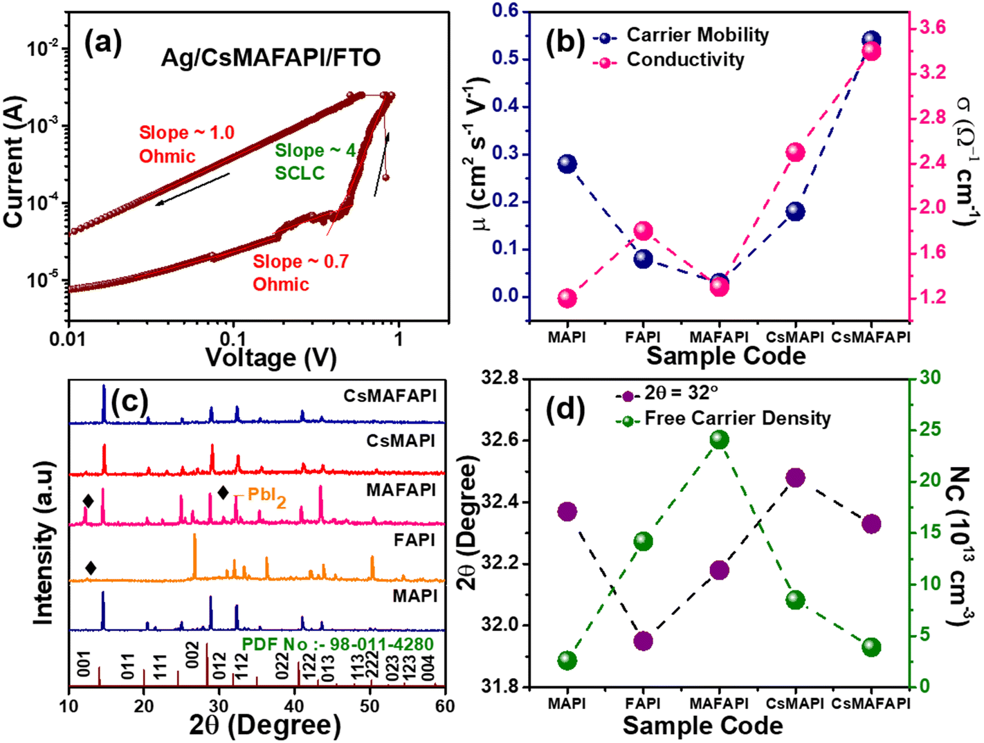 | ||
| Fig. 3 (a) logI vs. logV graph for the fabricated Ag/CsMAFAPbI3/FTO bipolar resistive switching devices with the (b) variation of carrier mobility with respect to the conductivity of the devices, (c) XRD pattern obtained for the APbI3 thin films recrystallized from aprotic solvents DMF:DMSO (8:2) upon annealing at 120 °C and (d) shift of 2θ = 32°, with respect to the free charge carrier concentration in the devices. | ||
| Carrier dynamics | N t (cm−3) | μ h (cm2 s−1 V−1) | σ (Ω−1 cm−1) | N c (cm−3) | D (×10−7 m2 s−1) |
|---|---|---|---|---|---|
| MAPI | 7.1 × 10¹¹ | 0.16 | 1.2 × 10⁻⁶ | 1.2 × 10¹³ | 0.11 |
| FAPI | 21 × 1011 | 0.10 | 1.8 × 10⁻⁶ | 11 × 1013 | 2.4 |
| MAFAPI | 41 × 1011 | 0.03 | 1.3 × 10⁻⁶ | 21 × 1013 | 85 |
| CsMAPI | 9.7 × 10¹¹ | 0.23 | 2.5 × 10⁻⁶ | 6.7 × 10¹³ | 5.6 |
| CsMAFAPI | 7.6 × 10¹¹ | 0.69 | 3.4 × 10⁻⁶ | 3 × 10¹³ | 0.17 |
Accordingly, the inorganic–organic cation mixture possessed the lowest trap density (7.6 × 1011 cm−3) attributed to the adequate tolerance factor (t), stable perovskite structure, and enhanced crystallinity, as observed from XRD. In contrast, FAPI and mixed organic cation MAFAPI holds higher trap densities of 21 × 1011 and 41 × 1011 cm−3, respectively, owing to the disorders and defects present in them, these results are corroborating the thin film XRD. Further, the values obtained are analogous with previous polycrystalline thin film trap density values obtained for MAPI.40–43 At higher voltages, the memory devices are observed to exist as in child's region, hence according to Mott–Gurney's law,
 | (1.2) |
Fig. 3c shows the XRD pattern obtained for the various cation-doped APbI3 (A = MA+, FA+, MAFA+, CsMA+, and CsMAFA+) nanoscale thin-film cast on the FTO-coated substrates. The introduction of MA+, CsMA+, and CsMAFA+ cations into the A-site of the APbI3 perovskite nanoscale thin-film is observed to retain its high-pure crystallinity and no additional peaks were observed for secondary phases. However, when FA+ was mixed with MA+ and allowed to recrystallize into MAFA+ nanoscale thin film, impurity peaks began to show, probably due to the co-existence of δ-FAPI with the α-FAPI phase at room temperature.45 Similarly, the FAPI nanoscale thin film showed major peaks of the unfavourable PbI2 phase on recrystallization owing to the phase change of FAPI from α-FAPI to δ-FAPI phase at room temperature.45
The concentration of free charge carriers (Nc) in the device influences the electrical and optical response of the device and can be estimated by the following relation,
 | (1.3) |
It can be observed that the Nc values are larger in FAPI corroborating with the larger cation size of FA+ and the presence of secondary phases in the nanoscale thin film. Fig. 3d depicts the shift of 2θ = 32° with respect to the charge carrier concentration. The large cation FA+ and mixed organic cation MAFA+ not only indicate a broader shift in the (012) plane but also affect the device performance owing to the presence of more free-charge carriers. The conductive filament (CF) formation in MHP-based resistive switching memory devices majorly depends on Nc. Thus, the charge transport kinetics further affirms the influence of A-site cation rotation on the optoelectronic performance of the perovskite-based nanoscale devices and their structure stability.39
Endurance properties and FTIR studies
The endurance test of the devices is another important resistive switching parameter. Fig. 4a–e, displays the endurance performance of the various cation-doped APbI3 (A = MA+, FA+, MAFA+, CsMA+, and CsMAFA+) perovskite ORSNVB memory devices. Fig. 4a demonstrates the endurance of MAPI showing 1500 cycles. However, when the A-site was substituted with the large cation FA+, the FAPI memory device hardly withstood 1200 cycles (Fig. 4b), demonstrating poor performance. The presence of a secondary phase in FAPI may have led to the formation of permanent CFs, or stochastic rupture of CFs due to the prompt recombination of charge carriers, thereby disrupting the switching performance.45Fig. 4c depicts the endurance performance of the ORSNVB device when both MA+ and FA+ were homogeneously mixed to achieve a MAFAPI memory device. The endurance is increased slightly to 1300 cycles probably attributed to the comparatively adequate tolerance factor and crystallinity of the MAFAPI nanoscale thin film. Interestingly, when the inorganic cation Cs+ was introduced along with the organic MA+ cation in the A-site of the APbI3 nanoscale thin film to achieve the CsMAPI memory device, the endurance cycles was drastically increased to 3500 cycles (Fig. 4d). Similarly, the influence of the inorganic cation ‘Cs’ with rather small radii can be observed with the triple cation perovskite CsMAFAPI with CsMAFA+ in the A-site of the perovskite, exhibiting 5000 cycles without any deterioration (Fig. 4e). The improved endurance ability of the CsMAFAPI bipolar resistive switching memory device could be assigned to the improved carrier mobility and decreased recombination effect at the grain boundaries.45,46 The statistical distribution of variation in the switching performance of the Ag/CsMAFAPI/FTO device with respect to device-to-device (D/D) performance and cycle-to-cycle (C/C) performance exhibit the average (μ) values of VSET and VRESET to be 0.37, −0.4, 0.37, and −0.5 V respectively, with standard deviation (σ) of 9.3, 10.6, 9.3 and 9.8% respectively as shown in Fig. 4f. The statistical analysis for the MAPI, FAPI, MAFAPI, and CsMAPI devices are provided in Fig. S6.†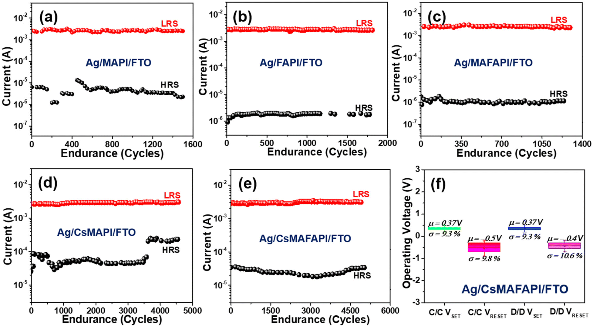 | ||
| Fig. 4 Endurance performance for (a) Ag/MAPI/FTO (b) Ag/FAPI/FTO (c) Ag/MAFAPI/FTO, (d) Ag/CsMAPI/FTO and (e) Ag/CsMAFAPI/FTO memory devices with (f) the statistical variation in operational voltages upon device-to-device (D/D) and cycle-to-cycle (C/C) performance. | ||
Fig. 5a shows the FTIR spectra obtained for the APbI3 samples synthesized via the MW-ST method recorded in the range of 400 to 2500 cm−1. The predominant and relatively high-intensity vibrations around 910 cm−1 correspond to CH3–NH3 rocking, of the MA+ cation, while the characteristic peak of the organic–inorganic perovskite occurs at 1459 cm−1 belonging to the C–H bending vibrations.47 In the case of incorporation of FA+ cation, the predominant peak occurring at 588 cm−1 belongs to the vibrations around the N–H bond, and the peak around 1700 cm−1 belongs to C![[triple bond, length as m-dash]](https://www.rsc.org/images/entities/char_e002.gif) N vibrations.48
N vibrations.48
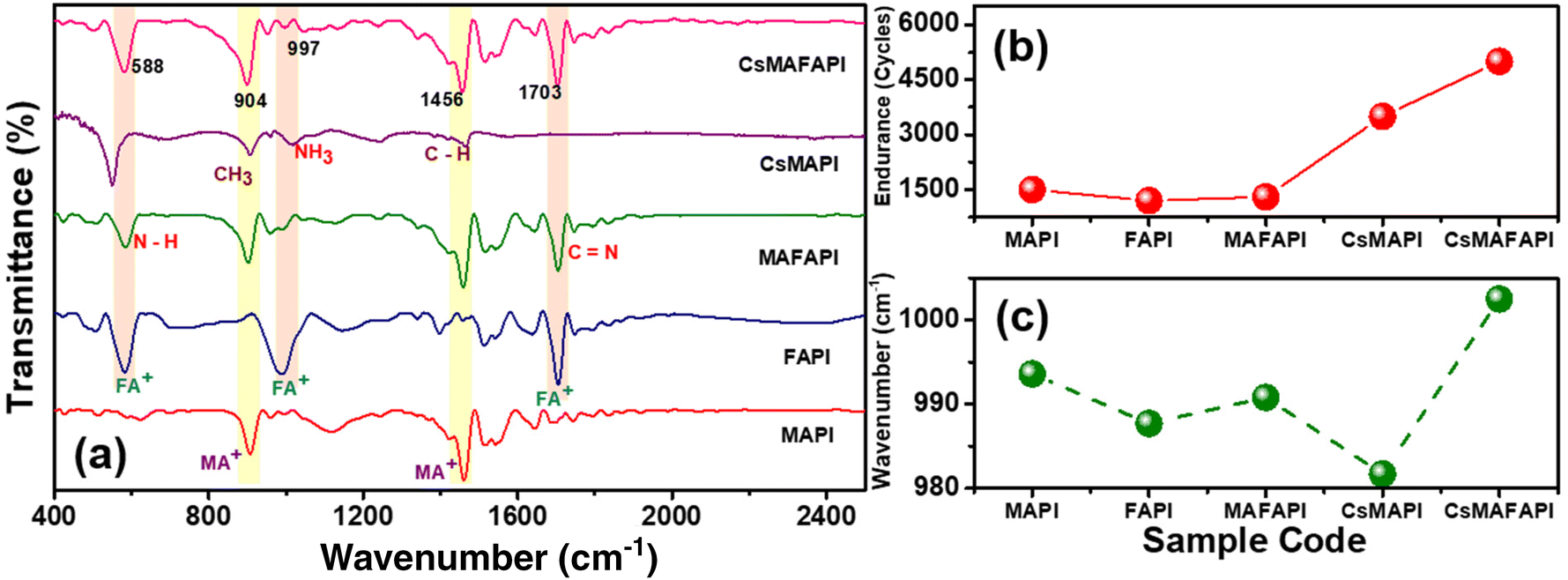 | ||
| Fig. 5 (a) FTIR spectra for the MW-ST synthesized APbI3 (A = MA+, FA+, MAFA+, CsMA+ and CsMAFA+) metal halide perovskites with (b) the endurance cycles for the fabricated devices of configuration of Ag/APbI3/Ag with (c) the shift of γ(C–N) vibrations. | ||
The shift in the frequency range of the synthesized perovskites can be assigned to the modification of the electrostatic and chemical association between the A-site cation and the octahedral cage (Fig. 5c). Analogous to our report, shifts related to Raman spectra have been reported earlier.49 Moreover, the peak shifts can be directly associated with the enhancement in bond strength, and the observed reduction in the distance between the A-site cation and the inorganic octahedra PbI6− could contribute towards better interaction and thus, improvement in the device performance.50
Additionally, the composition of the A-site cation affects the N+–X− interaction of the cation with the inorganic PbI6 octahedral cage.51 Considering the presence of MA+ and FA+ cations in the various organic and inorganic cation-doped APbI3 perovskite powders, the interaction of the A-site cation on the bond length and force constant of the CH3–NH3+ (MA+) and CH–(NH2)2+ (FA+) molecules was estimated using the relation between the vibrational frequency, ϑ of different bond stretching.45Table 2 and Table S4,† summarize the estimated bond lengths and force constant values according to eqn (1.4) and (1.5),
 | (1.4) |
 | (1.5) |
| APbI3 perovskite material | Wavenumber (cm−1) | Force constant k (N cm−1) | Bond length (Å) | |||
|---|---|---|---|---|---|---|
| ρ(CH3) | v a(N–C–N) | ρ(CH3) | v a(N–C–N) | ρ(CH3) | v a(N–C–N) | |
| MAPI | 908.4 | — | 1.175 | — | 2.436 | — |
| FAPI | — | 1702.21 | — | 6.700 | — | 1.646 |
| MAFAPI | 902.6 | 1704.56 | 1.172 | 6.713 | 2.438 | 1.645 |
| CsMAPI | 905.4 | — | 1.173 | — | 2.437 | — |
| CsMAFAPI | 899.6 | 1705.07 | 1.169 | 6.714 | 2.440 | 1.363 |
The stretching vibrations occurring at 940 and 1700 cm−1 denote the interaction between I− and the organic cation (MA+ and FA+). Herein, the contraction of the cationic bond length leads to increased Pb–I bending thus, enhancing the interaction between the A-site cation and the inorganic PbI6 octahedral framework.48 The lowest bond length obtained from the IR vibration for MAPI [2.436 for ρ(CH3)] and CsMAFAPI [1.363 for va(N–C–N)], denotes an ordered and stable structure, further corroborating the device performance and structural stability seen from the XRD study.47–49 Indeed, the variation in bond lengths, the tolerance factor, and structure stability substantially influence the optoelectronic properties and device performances.
The enhancement of the endurance cycles of the devices with respect to the incorporation of the cation with varied ionic radii is provided in Fig. 5b. Further, we also investigated the structural stability of APbI3 (A = MA+, FA+, MAFA+, CsMA+, and CsMAFA+) perovskites under high humid conditions (∼65 ± 5%, Pondicherry, India) by keeping all samples in ambient condition for 5 months, FTIR spectra of the samples of APbI3 metal halide perovskite powders showed no degradation, as shown in Fig. S7.†
Retention properties and conduction mechanism
Fig. 6a–e compares the effect of the various organic and inorganic cations doping in the APbI3 memory devices on the retention properties. In accordance with the endurance property, the organic ‘FA+’ cation-based ORSNVB memory devices with A = FA+ displayed poor retention properties of 2.7 × 10⁴ s with a low LRS/HRS resistance ratio of 20 (Fig. 6b and c). However, when MA+ is substituted in the A-site of APbI3, it retained the memory for 3 × 10⁴ s (Fig. 6a), further confirming the need for phase purity as well as minimum tolerance factor to achieve excellent resistive switching performance in accordance with the FTIR and XRD studies. Similarly, when MA+ is alloyed with FA+ to form MAFAPI, the switching property was retained for a slightly higher period of 3.2 × 10⁴ s. Remarkably, on the addition of the inorganic cation Cs+ along with the organic cations MA+ and MAFA+ to obtain CsMAPI and CsMAFAPI-based ORSNVB memory devices, the devices exhibited an enhanced retention of 6 × 10⁴ s (Fig. 6d and e) comparable with that of pure inorganic oxide memory devices, further confirming the necessity of A-site cation modulation for efficient device performance. The fluctuations in the retention data may be related to the degree of insulating characteristics of the APbI3 material corresponding to its composition with respect to the varied cation dopants. Further, poor coverage and the presence of pinholes in FAPI and the MAFAPI-based memory devices make them prone to high-humid atmospheric conditions. Thus, the uneven variation of the electric field within the APbI3 nanoscale layer can be attributed to the stochastic formation and rupture of conductive filaments.43 In addition, the trapping/de-trapping of electrons in the defect states cannot be ignored, provided secondary phase presence in FAPI and MAFAPI-based ORSNVB memory devices, as observed from the XRD studies. Further, the discharge of inevitable parasitic capacitance elements during the prompt resistance transitions can induce transient overshoots through the CFs, especially from grain boundaries.36–45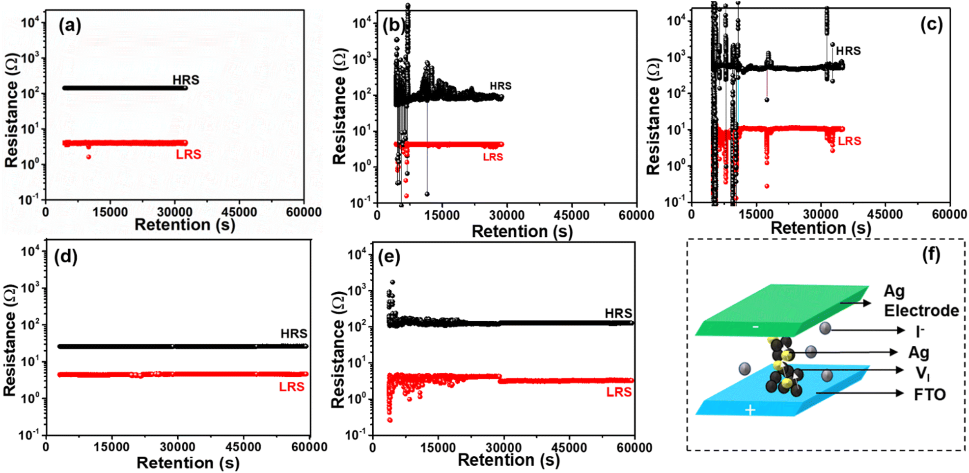 | ||
| Fig. 6 Retention properties of (a) Ag/MAPI/FTO (b) Ag/FAPI/FTO (c) Ag/MAFAPI/FTO, (d) Ag/CsMAPI/sFTO and (e) Ag/CsMAFAPI/FTO memory devices with the (f) conduction mechanism for the ORSNVB memory device. | ||
A vacancy-mediated conduction mechanism is proposed for the Ag/APbI3/FTO devices, where, VI with a low activation energy of migration forms a conductive pathway.46 The diffusion coefficient (D) is determined from the earlier estimated charge carrier mobility (μ) at room temperature (T) using the relation,47
 | (1.6) |
The carrier diffusion coefficients were calculated as 0.11 × 10⁻⁷, 2.4 × 10⁻⁷, 85 × 10−7, 5.6 × 10⁻⁷ and 0.17 × 10⁻⁷ m2 s−1 for MAPI, FAPI, MAFAPI, CsMAPI, and CsMAFAPI resistive switching memory devices, respectively.
Interestingly the values lie in the range of the reported diffusion coefficient values (10−16 to 10−7 m2 s−1) for iodine vacancy VI, thus promoting a vacancy-filled conduction filament (CF) formation.51,52 Additionally, based on the logI vs. logV graph, the prompt conversion of conductive filament from ohmic to SCLC confirms the trap-assisted CF formation in APbI3-based ORSNVB memory devices. However, the negligible presence of the metallic Ag-based CFs can never be completely neglected (Fig. 6f). Further, the diffusion coefficient D, is directly proportional to the diffusion length, L ∝ √D, thereby directing a large diffusion length for MAPI and CsMAFAPI memory devices. Thus, the improved charge transport properties of the triple cation could be ascribed to the enhanced optoelectronic device performance of the memory devices.
MW-ST reaction kinetics and thermodynamics
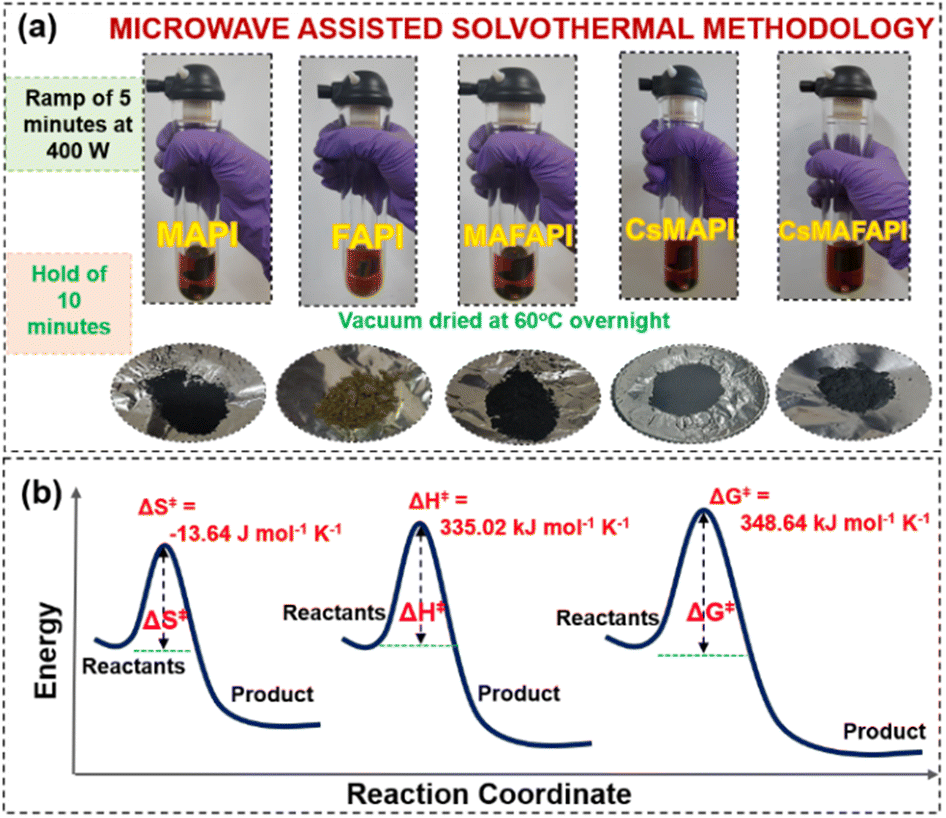
Furthermore, the properties of metal halide perovskite materials such as crystallinity, grain boundary and grain size, stoichiometry, and structural stability have to be optimised to achieve efficient optoelectronic performance.53 In this regard, powder processing of metal halide perovskites, prior to thin film processing is considered an effective approach to obtain phase-pure, and chemically and structurally highly stable perovskites with longer shelf-life.23Fig. 7a illustrates the microwave-assisted solvothermal (MW-ST) synthesis of APbI3 metal halide perovskites under high-humid ambient conditions without any inert gas atmosphere. Low-cost and non-toxic precursors such as lead acetate and isopropyl alcohol were used for the reaction in an isolated quartz vessel of the Anton Paar microwave reactor. An optimum power of 400 W was fixed with ramp time maintained for 5 min followed by 10 min of hold time (∼120 °C). An average autogenous pressure of ∼12 bar was generated inside the vessel, as measured by the reactor system. Upon microwave (MW) irradiation, the nucleation process was promptly initiated and the particle size gradually increased from its seed size. Subsequently, the velocity of the dipoles in the precursor mixture was also increased as they tried to align with the oscillating electromagnetic field provided by the reactor system.54 Thus, adequate thermal energy was created that facilitated the creation of “hot spots” that favoured burst nucleation as in the case of La Mer crystallization.50 Accordingly, the electromagnetic radiation, directly interacts with the reactants, thereby creating an energetic coupling at the molecular level, thus further enhancing the growth of the APbI3 metal halide perovskite powders.53,54 For a typical APbI3 metal halide perovskite synthesis, the conversion of reactants into their final products occurs as shown in eqn (1.7).| Pb(Ac)2 + 3HI + CH3NH2/A(Ac)2 → APbI3 + CH3COOH | (1.7) |
 | ||
| Fig. 7 (a) Microwave-assisted solvothermal (MW-ST) synthesis of the APbI3 metal halide perovskite powders with a comparison of (b) activation-free entropy ΔS‡, activation free enthalpy ΔH‡ and activation free energy ΔG‡ of the MW-ST synthesis of CsMAFAPI. | ||
The effect of MW-ST substitutional doping of cations in the A-site of the APbI3 perovskite structure was studied using thermodynamic parameters derived from the Eyring equation shown in eqn (1.8)
 | (1.8) |
 | (1.9) |
The ΔH‡ and ΔS‡ values were estimated from the slope and intercept respectively for the reaction rates plotted between 1/T and ln(k/T).
In a closed, isolated system, the activation-free energy ΔG‡ is obtained from eqn (1.10)
| ΔG‡ = ΔH‡ − S‡ΔT. | (1.10) |
Finally, the activation energy Ea for a solution process is given by eqn (1.11)
| Ea = ΔH‡ + RT. | (1.11) |
The activation-free energy ΔG‡ is observed to be the lowest for the inorganic–organic mixed cation-based perovskite, CsMAFAPI, which is 7 kJ lower than that for the homogenous organic cations-based MAPI and FAPI.20 The reduction in the activation-free energy could be further attributed to the reduced activation entropy ΔS‡. The activation enthalpy ΔH‡ contribute substantially towards improved reaction kinetics and energy saving. It could also be noted that, lesser ΔG‡ indicates the requirement of less energy for initiating the reaction and the negative value of ΔS‡ indicates the coherently directed energy that is utilized for the reaction without dissipation or scattering.54 The lowest ΔS‡ obtained for CsMAFAPI denotes the formation of a stable structure of the product, hindering the molecular movement and thereby reducing randomness.55Table 3, tabulates the estimated thermodynamic parameters obtained for the MW-ST synthesized APbI3 perovskites. The comparison of activation-free energy, activation-free enthalpy, and entropy for the formation of CsMAFAPI under MW-ST conditions are represented in Fig. 7b.
| Reaction parameter | MAPI | FAPI | MAFAPI | CsMAPI | CsMAFAPI | |
|---|---|---|---|---|---|---|
| T i = initial temperature at the start of reaction, TR = temperature at the end of ramp time and TH = temperature at the end of hold time. | ||||||
| Temperature (°C) | T i | 30 | 31 | 31 | 32 | 30 |
| T R | 67 | 65 | 66 | 61 | 69 | |
| T H | 112.7 | 111 | 111 | 109 | 101 | |
| Reaction time (min) | 15 | 15 | 15 | 15 | 15 | |
| Reaction rate (s−1) | 1 × 10⁻³ | 1 × 10⁻³ | 1 × 10⁻³ | 1 × 10⁻³ | 1 × 10⁻³ | |
| ΔG (kJ mol−1) | 355.4 | 354.9 | 354.7 | 356.2 | 348.6 | |
| ΔH (J mol−1) | 341.7 | 341.3 | 341.1 | 342.6 | 335.0 | |
| ΔS (J mol−1 K−1) | −13.64 | −13.64 | −13.64 | −13.64 | −13.62 | |
| E a (J mol−1) | 3196.6 | 3185.8 | 3175.8 | 3178.9 | 3160.2 | |
Fig. S8† shows the reliability of the multilevel storage capacity of the APbI3 memory devices tested with 30 cycles for compliance current (CC) set at 1, 10, and 100 mA. Regardless of the cation introduced, the ORSNVB memory devices displayed the multilevel property owing to the difference in the thickness of the CF formed by varying the CC. Further, the stability of the ORSNVB devices was tested after 50 days of storage under ambient conditions. Fig. S9† shows the semi-logarithmic curve with stable RESET but deteriorating SET, which could be due to the modification of the electric field in the presence of high humidity under ambient conditions. The change in SET with respect to surface defects further confirms the crucial role of defect vacancy-mediated CF formation in the APbI3 memory devices.55 Fig. S10† shows the photographs of the as-fabricated APbI3 thin films immediately after annealing and after 5 months of storage in ambient conditions under dark conditions.
Opto-electronic properties and photonic memory application
In order to explore the excellent photoelectric properties of the various cation-doped APbI3 (A = MA+, FA+, MAFA+, CsMA+, and CsMAFA+), memory devices, optical signals in addition to the electrical signals were explored for modulation, which adds another dimension to control the resistance of the memory device. The photoelectric performance of the ORSNVB memory devices upon cation doping was studied using a 100 mW cm−2 xenon lamp, with a compliance current (CC) of 1 mA. Prior to the switching characterization, the ORSNVB memory devices were stored in dark conditions, to achieve equilibrium. Fig. 8a–e shows the photoelectric performance of the ORSNVB memory devices examined using a xenon lamp. Despite the various-doped cations, the APbI3 memory devices showed ORSNVB memory behaviour under illumination with reduced VSET and increased VRESET. It could be observed that the HRS current was increased, which could be attributed to the spontaneous production of the electron–hole pairs within the APbI3 nanoscale absorber layer upon illumination.56 Additionally, the slightly reduced VSET voltage values can probably be due to the prompt extraction of photocarriers, which readily contribute towards reducing the operating voltage. However, upon illumination, VI vacancies move randomly, thus creating a high built-in electric field thus requiring an increased VRESET to dissociate the CFs.23 Thus, the variation in the operating voltage upon illumination attributed to the randomness of the halide vacancies migration, further confirms the presence of the VI-based CF formation for the resistive switching performance.55,56 Fig. S11† shows the endurance performance tested to explore the reliability of the devices under illumination. Fig. S12† gives the variation of electrical and optical endurance, showing lowered cycles with the addition of illumination, further confirming the dominating presence of the halide-vacancy-mediated CFs. Fig. S13† shows the cumulative plot for the distribution of operational voltages obtained under illumination for various ORSNVB memory devices fabricated. Corroborating with electrical switching performance and other physicochemical characterizations, the endurance performance remained weak for the APbI3 devices with A = FA+ and MAFA+ exhibiting fewer cycles and quicker rupture of CFs compared to MAPI and the inorganic cation included CsMAPI and CsMAFAPI-based ORSNVB memory devices. The results further imply the crucial role of the A-site cation in the APbI3 structure of perovskite materials towards the improvement of the device performance. Fig. 8f depicts the variation of VSET voltage obtained under electrical signals and when illuminated under ambient conditions. Table 4 summarizes the complete device performance of the fabricated Ag/APbI3/FTO (A = MA+, FA+, MAFA+, CsMA+, and CsMAFA+) non-volatile bipolar resistive switching memory devices.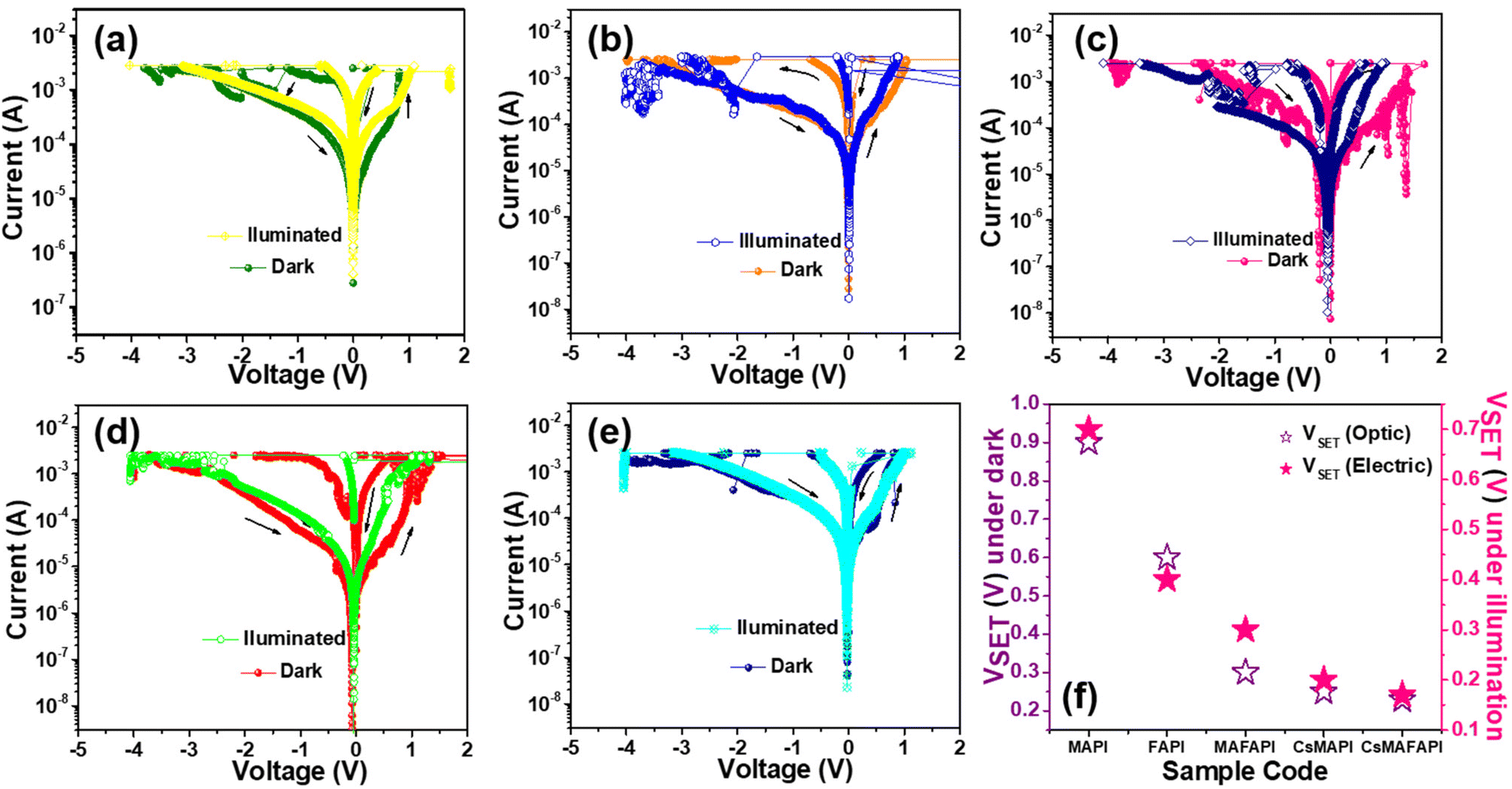 | ||
| Fig. 8 The semi-logarithmic resistive switching performance for (a) Ag/MAPI/FTO (b) Ag/FAPI/FTO (c) Ag/MAFAPI/FTO, (d) Ag/CsMAPI/FTO (e) Ag/CsMAFAPI/FTO memory devices under illumination and (f) variation of VSET for the Ag/APbI3/FTO devices under electric and optical stimuli. | ||
| APbI3 perovskite material | Dark | Illumination | |||
|---|---|---|---|---|---|
| V SET/VRESET (V) | Endurance (cycles) | Retention (s) | V SET/VRESET (V) | Endurance (cycles) | |
| MAPI | 0.6/−1.3 | 1500 | 3 × 10⁴ | 0.6/−2.0 | 1100 |
| FAPI | 0.7/−2.4 | 1200 | 2.7 × 10⁴ | 0.5/−1.7 | 800 |
| MAFAPI | 0.5/−1.7 | 1300 | 3.2 × 10⁴ | 0.3/−0.7 | 1200 |
| CsMAPI | 0.3/−0.8 | 3500 | 6 × 10⁴ | 0.2/−2.1 | 1300 |
| CsMAFAPI | 0.2/−0.7 | 5000 | 6 × 10⁴ | 0.2/−2.1 | 1800 |
The UV-vis absorption spectra of the as-synthesized APbI3 (A = MA+, FA+, MAFA+, CsMA+, and CsMAFA+) metal halide perovskite powders showed excellent absorption across the visible region as shown in Fig. S15a.† The band gap from the Tauc plot exhibited values according to the cationic radii 1.53, 2.3, 1.6, 1.59, and 1.53 eV for MAPI, FAPI, MAFAPI, CsMAPI, and CsMAFAPI, respectively (Fig. S15b†). The statistical distribution of operational voltages obtained for the fabricated ORSNVB memory devices under illumination with the standard mean and deviation is provided in Fig. S14.† The UV-vis absorption and PL-steady state for the nanoscale thin films recrystallized from the precursor solution of the as-synthesized APbI3 powders also showed a similar trend (Fig. S16a and b†). Similarly, the steady-state PL and TRPL were also investigated for the as-synthesized powders (Fig. S15c and d†).
The application of the ORSNVB memory device was further carried out for image recognition function and photonic memory application, by making use of a 5 × 5 planar array of CsMAFAPbI3 based ORSNVB memory device (Fig. 9). The image-recognizing ability of the fabricated ORSNVB device was studied under ambient conditions.57 Initially, the resistance of the individual memory element on the 5 × 5 planar Ag/CsMAFAPbI3/FTO memory device was measured at room temperature and that data are shown in Fig. 9(i). Subsequently, +5 V was given, to make the ORSNVB memory device attain the SET process at a low resistance state the resistance of each memory cell at this point was measured to confirm the uniformity of the planar array, Fig. 9(ii). The measured resistance was low (<250 Ω). Immediately, the ORSNVB memory device was exposed to the xenon lamp (λ = 450 nm), with customized masks of the alphabet to be remembered blocking the light to the memory cell. The light exposure was given for 300 s, followed by a prompt resistance measurement Fig. 9(iii). The specific areas masked from light achieved the RESET process, while the exposed area continued to be in the SET process. The resistance of the cells with blocked illumination continues to have increased resistance owing to the diffusion effect of VI-conductive filaments. The resistance of the individual cells was measured immediately after the exposure to give a promising recognition ability under highly humid ambient conditions. Further, the resistances were measured after 600 s of the interval to achieve a reliable result (Fig. 9(iv)), which guarantees the potential utilization of metal halide perovskites-based ORSNVB memory devices for reliable photonic memory that could be beneficial for innovative optoelectronic systems in security, artificial vision, and other integrated systems.
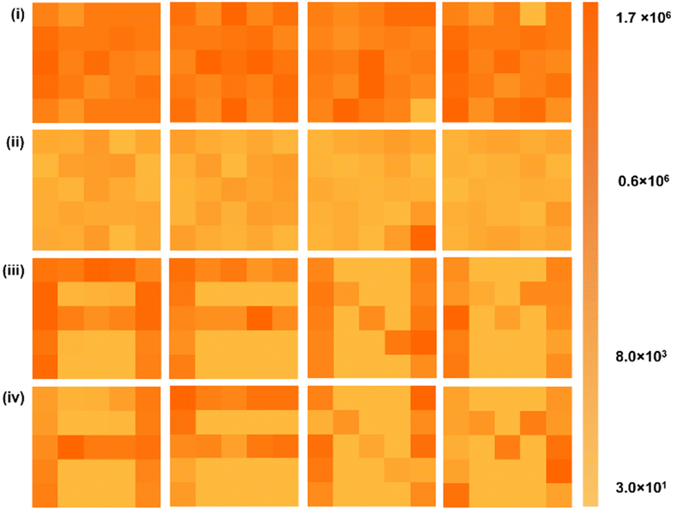 | ||
| Fig. 9 Image recognizing and memorizing performance of the Ag/CsMAFAPI/FTO memory devices (5 × 5 array) under illumination. (i) HRS state of the device at initial condition (ii) resistance state after SET process is attained (iii) resistance state after 300 s of illumination and (iv) resistance state after 600 s of rest time. | ||
A-site cation-induced SEM morphology studies
The influence of various organic and inorganic cations doped in the A-site of the APbI3 lattice under MW-ST conditions was investigated using SEM analysis. Here, the MW-ST synthesis process was conducted inside a quartz vessel and the reaction was initiated immediately after the reactor generated microwave radiation. Parameters such as temperature, pressure, solvent, thermodynamic parameters, and kinetics generally influence the growth mechanism of the crystals.59 In our MW-ST method, autogenous pressure is generated inside the vessels, favouring quick nucleation.60Fig. 10a shows the schematic illustration of the variation in morphology with respect to various cations substituted in the A-site of the metal halide perovskite Fig. 10b–f depicts the SEM images of the APbI3 metal halide perovskite samples with respect to the cations introduced into the A-site of APbI3 perovskites. Fig. 10b, reveals cube-like polyhedron morphology of the SEM images of APbI3 with A = MA+ (MAPI). The flat facets of MAPI can be attributed to the preferred growth along the (220) plane observed from the intense peak of (220) at 2θ = 28° peak splitting. Similar cube-like polyhedron morphology owing to the influence of the MA+ cation in the A-site is seen in the SEM images of CsMAPI, denoting the predominant role of MA+ cation promoting the cube-like polyhedron morphology. Fig. 10c on the other hand, shows a rod-like morphology when FA+ cation is introduced in APbI3, (FAPI). The rod-like morphology can be owed to the enhanced growth along the (004) and slow growth along the (220) plane at 2θ = 28° peak splitting. Further, the influence of FA+ can be observed in the mixed cation MAFA+ perovskite MAFAPI (Fig. 10d), the mixed organic cation-based MAFAPI perovskite shows, agglomerated truncated cubes with facets etched at the centre. The presence of voids in the facets can be addressed by the faster growth of the outer crystal planes.58 The separation of peak splitting at 2θ = 28°, is negligible and the growth rate is almost the same along the (220) and (004) planes, thus obtaining an agglomerated as well etched morphology. Although the equimolar concentration of the precursors was utilized for the synthesis, the dominance of MA+ cation in the morphology of mixed MAFA+ perovskite can be ascribed to the infiltration of MA+ cation with smaller radii into the octahedral cage easily than the large FA+ cation during crystallization, corroborating with the XPS results (Fig. S17a–f†). The dominance of the MA+ cation is clearly visible by the relative intensity and areas of the deconvoluted peak intensities of MA+ and FA+ cation in the N 1s core–shell spectra (Fig. S17f†). Interestingly, the size-mismatched structure of CsMAPI and CsMAFAPI on the addition of Cs+ (smaller ionic radii) with large ionic radii possessing organic cation (MA+ and MAFA+) into the A-site of APbI3, showing mixed morphology of rods and cubes (Fig. 10e). The coexistence of rods and cubes can be ascribed to the influence of the inorganic and organic cations Cs+ and MA+ separately, wherein, initially, MA+-influenced cubes are formed and later self-assembled to form rods. Similarly, in the case of the triple cation CsMAFAPI, truncated cubes of MAFAPI are observed with neatly arranged rods (Fig. 10f). Again, the inorganic cation Cs+ and organic cations MAFA+ influence the self-assembled rod-like morphology of the metal halide perovskite. These morphologies demonstrate the advantages of both cube-like and rod-like structures enabling high surface area and better particle–particle interconnection, which in turn offers prompt electron transport, favouring the electrochemical switching performance.58–61 Therefore, we can conclude that various organic and inorganic cations doped into the A-site of APbI3 perovskite lattice influence the morphology of metal halide perovskites under MW-ST conditions, owing to the disparity in their ionic radii. The variation in morphology with respect to various cations is schematically illustrated in Fig. 10a. Additional SEM images for the MHP powders are provided in Fig. S18.† The influence of the cation substitution in the A-site of the APbI3 (A = MA+, FA+, MAFA+, CsMA+, and CsMAFA+) perovskite on the thermal stability was analysed using the TGA analysis and is provided in Fig. S19,† wherein, in the case of the incorporation of the inorganic cation Cs+ into MAPI and MAFAPI, both CsMAPI and CsMAFAPI showed continuous mass loss after 350 °C, depicting the strong coordination and stability of the material.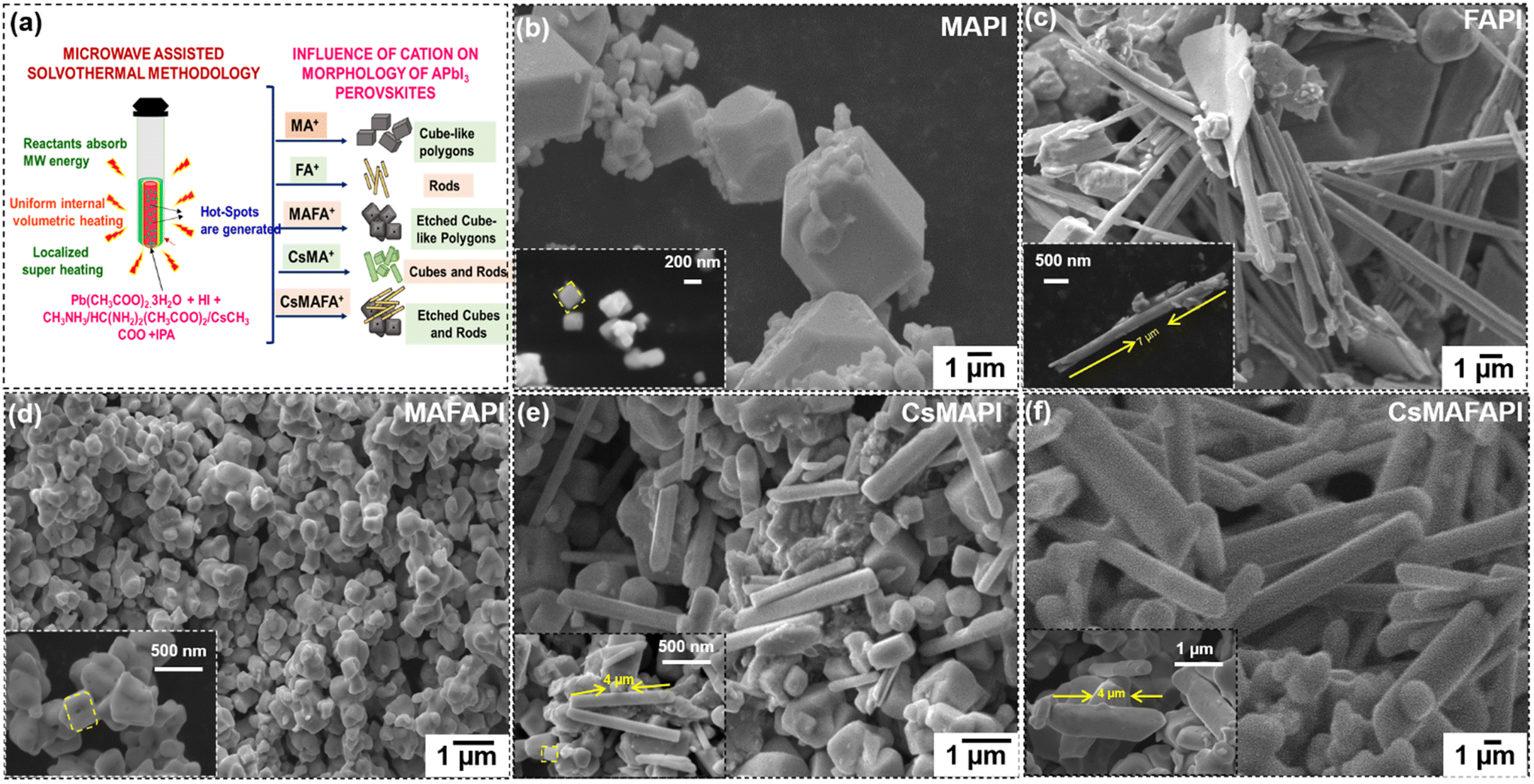 | ||
| Fig. 10 (a) Schematic illustration of influence of cation-induced morphology change in APbI3 (A = MA+, FA+, MAFA+, CsMA+ and CsMAFA+) metal halide perovskites. (b–f) SEM images of various cations doped in the A-site of APbI3 metal halide perovskites induced morphology changes (b) cube-like polyhedrons when A = MA+ (c) rods observed with A = FA+, (d) truncated cube-like polyhedrons when A = MAFA+ (e) mixed morphology of cubes with rods when A = CsMA+ and (f) mixed morphology of rods and truncated cube-like polyhedrons when A = CsMAFA+ in the A-site of APbI3 metal halide perovskites. | ||
On the other hand, the surface morphology of the various organic and inorganic cation-doped APbI3 (A = MA+, FA+, MAFA+, CsMA+, and CsMAFA+) self-assembled nanoscale thin film upon annealing the spin-coated precursor solution of MHP powder dissolved in aprotic solvents DMF:DMSO (8:2) was investigated using SEM studies. The images indicate variation in morphology corresponding to the introduction of different organic and inorganic cations. On a similar note, dense polycrystalline films, with larger grain sizes were formed upon the addition of the inorganic cation Cs+ with the organic cations in CsMAPI and CsMAFAPI. Fig. S20a–c† shows, poor film coverage and inhomogeneous morphology in thin films of MAPI, FAPI, and MAFAPI, which could be attributed to the uncontrolled nucleation and recrystallization of the precursor solution on FTO upon annealing at 120 °C. The non-uniformity causes roughness and consequent current loss leading to poor device performance as observed in Fig. 2b–f. Platelet-like morphology was observed for MAPI nanoscale thin film with irregularities and pinholes (Fig. S20a†). However, FAPI shows large pinholes and uneven coverage compared to other thin films, thereby corroborating its poorer device performance (Fig. S20b†). In the case of the mixed organic cation-based MAFAPI, polygonal grains emerge with tiny pinholes (Fig. S20c†). When the inorganic Cs+ was introduced with the organic cation CsMAPI, the pinholes are negligible owing to the presence of mixed morphology of rods above and polygonal grains beneath (Fig. S20d†). It is noteworthy to observe that when Cs+ was introduced with mixed organic cation CsMAFAPI, a typical polycrystalline perovskite thin film with a large polygonal grain size was observed (Fig. S20e†). The decreased grain boundaries and improved coverage may have contributed to the enhanced endurance and retention properties of the Ag/CsMAFAPI/FTO memory device. Since device performance is largely dependent on thin film morphology, further optimization of the device architecture by improving the surface quality via interlayers and base layers could drastically enhance the performance of the MW-ST-synthesized perovskite materials for non-volatile resistive switching memory devices. Fig. S21a–e† provides the cross-sectional images of the Ag/APbI3/FTO devices determining the thickness. The importance of microwave-assisted solvothermal (MW-ST) preparation of APbI3 metal halide perovskites for memory devices is compared with other reported memory devices in Table S5.†
Conclusions
In summary, we have successfully demonstrated a rapid and sustainable microwave-assisted solvothermal (MW-ST) method to synthesize various organic and inorganic cation-doped APbI3 (A = MA+, FA+, MAFA+, CsMA+, and CsMAFA+) metal halide perovskite powders in 10 minutes without requiring any inert gas atmosphere under high-humid ambient conditions. In correlation with structure, morphology, and optoelectronic properties, the charge transport properties were also estimated to elucidate the influence of various organic and inorganic cation doping in the A-site of the APbI3 perovskite structure. Dopant-induced morphology change from cube-like polyhedrons to intermixed cubes and rods was observed, owing to the disparity in the cationic radii of the dopants. Subsequently, the as-synthesized APbI3 powders were dissolved in aprotic solvents (DMSO:DMF, 8:2) and were allowed to recrystallize into a nanoscale self-assembled thin film via facile spin coating for constructing an optoelectronic resistive switching non-volatile bipolar (ORSNVB) memory device. A facile two-terminal Ag/APbI3/FTO configured ORSNVB memory devices were systematically investigated. Indeed, the introduction of inorganic cation Cs+ with the organic cation-MA+ in the A-site, to form CsMAFAPI and CsMAPI-based ORSNVB memory devices showed remarkable endurance (3500, and 5000 cycles, respectively) and enhanced retention properties (60000 s). The results concluded that the ionic radii of the various cations doped in the A-site of APbI3 influence the tolerance factor and promote enhancement in the overall electronic properties of the device performance, owing to the strain induced in the nanoscale thin films. Intriguingly, the MW-ST method enabled crystalline APbI3 metal halide perovskite powders to remain stable for ∼5 months without encapsulation and protection. Photonic image recognition and memory application were demonstrated using the Ag/CsMAFAPI/FTO-based ORSNVB memory device with a retention of 600 s. Thus, the present work sheds light on integrating the strategies of innovative MW-ST synthesis and incorporation of inorganic cations for improved ORSNVB performance towards obtaining various structurally and operationally stable perovskites for their potential optoelectronic applications in artificial intelligence (AI), neuromorphic computing, artificial vision (AV) and photonic memory (PM).
Experimental section
Microwave-assisted solvothermal synthesis of APbI3 (A = MA+, FA+, MAFA+, CsMA+ and CsMAFA+) metal halide perovskite powders
The various cation-doped APbI3 (A = MA+, FA+, FAMA+, CsMA+, and CsFAMA+) perovskite powders were prepared according to our previous report.23 The precursor solution contained lead acetate and hydroiodic acid in the radio 1:3. Subsequently, 30 mL of isopropyl alcohol was added and yellow precipitates were obtained. Stoichiometry amounts of the cation precursor (methylamine solution, formamidine acetate, cesium acetate) were slowly added to the reaction mixture until black precipitates appeared. The solution was then transferred to an isolated quartz vessel for homogeneous and uniform heating in an Anton Paar Microwave Reactor system. The program was set at 2.45 GHz frequency with the program pre-set for a 5 min ramp and 10 min hold. The internal temperature and the autogenous pressure developed inside each vessel were monitored automatically. The average pressure inside the vessel was ∼12 bar. The reactor's built-in cooling system was utilized to bring the vessels to room temperature automatically. The back precipitates obtained were washed twice with isopropyl alcohol before drying at 60 °C under vacuum overnight. The as-synthesized perovskite powders were then collected and stored for characterization and applications. The samples were named according to the cation introduced in the A-site of the APbI3 as MAPI, FAPI, MAFAPI, CsMAPI, and CsMAFAPI.
Device fabrication
:DMSO (8:2), obtaining a 1 M precursor solution for fabricating the ORSNVB memory device. The prepared precursor solution was then allowed to recrystallize into APbI3 nanoscale thin film layer by spin coating, followed by annealing at 120 °C.62–64 A two-step spin speed of 500 rpm for 30 s followed by 1000 rpm for 15 s was used to obtain a uniformly-coated smooth film on the FTO bottom electrode. Further, the top contacts of silver were coated to complete the device.
Author contributions
Twinkle George designed the concept and carried out the experiments under Prof. A. Vadivel Murugan's supervision. The authors discussed the analytical results and co-wrote the manuscript.Conflicts of interest
There are no conflicts to declare.Acknowledgements
The authors express their gratitude towards the Department of Science and Technology (DST), Government of India, New Delhi, Clean Energy Research Initiative (CERI) Program under project no. DST/TM/CERI/C-264(G) for the financial support. The authors give special thanks to Central Instrumentation Facility (CIF), Pondicherry University, for the timely characterization of materials.Notes and references
- Y. Wang, Z. Lv, L. Zhou, X. Chen, J. Chen, Y. Zhou, V. A. L. Roy and S.-T. Han, J. Mater. Chem. C, 2018, 6, 1600 RSC.
- B. Li, W. Hui, X. Ran, Y. Xia, F. Xia, L. Chao, Y. Chen and W. Huang, J. Mater. Chem. C, 2019, 7, 7476 RSC.
- H. Kim, J. S. Han, S. G. Kim, S. Y. Kim and H. W. Jang, J. Mater. Chem. C, 2019, 7, 5226 RSC.
- Y.-R. Jeon, Y. Abbas, A. S. Sokolov, S. Kim, B. Ku and C. Choi, ACS Appl. Mater. Interfaces, 2019, 11, 23329 CrossRef CAS PubMed.
- H.-R. Xia, W.-T. Sun and L.-M. Peng, Chem. Commun., 2015, 51, 13787 RSC.
- M.-J. Lee, C. B. Lee, D. Lee, S. R. Lee, M. Chang, J. H. Hur, Y. B. Kim, C. J. Kim, D. H. Seo, S. Seo, U. Chung, I. Yoo and K. Kim, Nat. Mater., 2011, 10, 625 CrossRef CAS PubMed.
- E. Yoo, M. Lyu, J.-H. Yu, C. Kang, Y. Choi and L. Wang, J. Mater. Chem. C, 2016, 4, 7824 RSC.
- T. Guanqi and Y. Feng, J. Semicond., 2021, 42, 101606 CrossRef.
- Y. J. Yung and K. Y. Jin, J. Semicond., 2021, 42, 101608 CrossRef.
- C. Qi, W. Wei, X. Shenqiang, C. Yi-bing, H. Fuzhi and X. Wanchun, ACS Appl. Mater. Interfaces, 2019, 30, 27145–27152 Search PubMed.
- X. Weidong, L. Gang, T. Chen, Z. Jiandong, L. Xiaoke, X. Xiang, L. Y. Wen, G. Feng and H. Wei, Adv. Funct. Mater., 2018, 28, 1802320 CrossRef.
- P. Shu, X. Cao, Y. Du, J. Zhou, J. Zhou, S. Xu, Y. Liu and S. Cao, J. Mater. Chem. C, 2020, 8, 12865 RSC.
- B. Hwang, C. Gu, D. Lee and J. S. Lee, Sci. Rep., 2017, 7, 43794 CrossRef PubMed.
- Y. Kim, C. Bae, H. S. Jung and H. Shin, APL Mater., 2019, 7, 081107 CrossRef.
- Y. Hu, E. M. Hutter, P. Rieder, I. Grill, J. Hanisch, M. F. Ayguler, A. G. Hufnagel, M. Handloser, T. Bein, A. Hartschuh, K. Tvingstedt, V. Dyakonov, A. Baumann, T. J. Savenije, M. L. Petrus and P. Docampo, Adv. Energy Mater., 2018, 1703057 CrossRef.
- C. Cuhadar, S. G. Kim, J. M. Yang, J. Y. Seo, D. Lee and N.-G. Park, ACS Appl. Mater. Interfaces, 2018, 10, 29741–29749 CrossRef CAS PubMed.
- Y. Huang, Z. Zhao, C. Wang, H. Fan, Y. Yang, J. Bian and H. Wu, Sci. China Mater., 2019, 62, 1323–1331 CrossRef CAS.
- S. Y. Kim, D. A. Park and N.-G. Park, ACS Appl. Electron. Mater., 2022, 4, 2388–2395 CrossRef CAS.
- S. Attique, N. Ali, R. Khatoon, S. Ali, A. Abbas, Y. Yu, J. Hou, B. Cao, H. Wu and S. Yang, Green Chem., 2020, 22, 3608 RSC.
- K. Thesika and A. Vadivel Murugan, Inorg. Chem., 2020, 59, 6161–6175 CrossRef CAS PubMed.
- T. Bonnisa Magdaline and A. Vadivel Murugan, Dalton Trans., 2020, 49, 6227–6241 RSC.
- S. Praneetha and A. Vadivel Murugan, RSC Adv., 2013, 3, 25403–25409 RSC.
- T. George and A. Vadivel Murugan, ACS Appl. Mater. Interfaces, 2022, 14, 51066–51083 CrossRef CAS PubMed.
- D. Caner, T. Shaun, K. N. Houk, Y. Yang and Y. Illhan, Nano Res., 2022, 15, 5746–5751 CrossRef.
- J. Brown, C. Jinguo, Y. Ruiban, C. Bing, W. Congcong and Z. Xiaojia, Adv. Energy Sustainability Res., 2022, 2200143 Search PubMed.
- D. J. Xue, Y. Hou, S. C. Liu, M. Wei, B. Chen, Z. Huang, Z. Li, B. Sun, A. H. Proppe, Y. Dong, M. I. Saidaminov, S. O. Kelly, J. S. Hu and E. H. Sargent, Nat. Commun., 2020, 11, 1514 CrossRef CAS PubMed.
- K. Nishimura, D. Hirotani, M. A. Kamarudin, Q. Shen, T. Toyoda, S. Iikubo, T. Minemoto, K. Yoshino and S. Hayase, ACS Appl. Mater. Interfaces, 2019, 11, 31105–31110 CrossRef CAS PubMed.
- B. Hwang and J. S. Lee, Nanoscale, 2018, 10, 8578 RSC.
- S. Premkumar, K. Kundu and S. Umapathy, Nanoscale, 2019, 11, 10292 RSC.
- W.-G. Li, H.-S. Rao, B.-X. Chen, X.-D. Wang and D.-B. Kuang, J. Mater. Chem. A, 2017, 5, 19431 RSC.
- E.-S. Choi, J.-M. Yang, S.-G. Kim, C. Cuhadar, S.-Y. Kim, S. H. Kim, D. Lee and N.-G. Park, Nanoscale, 2019, 11, 14455 RSC.
- S. Parveen, K. K. Paul and P. K. Giri, ACS Appl. Mater. Interfaces, 2020, 12, 6283–6297 CrossRef CAS PubMed.
- Y. Sun, J. Peng, Y. Chen, Y. Yao and Z. Liang, Sci. Rep., 2017, 7, 46193 CrossRef CAS PubMed.
- J. H. Heo, D. H. Shin, S. H. Moon, M. H. Lee, D. H. Kim, S. H. Oh, W. Jo and S. H. Im, Sci. Rep., 2017, 7, 16586 CrossRef PubMed.
- D. Zhang, T. Zhu and T. Pauporte, ACS Appl. Energy Mater., 2020, 3, 10349–10361 CrossRef.
- K. Shubhakar, S. Mei, M. Bosman, N. Raghavan, A. Ranjan, S. J. O'Shea and K. L. Pey, Microelectron. Reliab., 2016, 64, 204–209 CrossRef CAS.
- G. S. H. Thien, M. A. M. Sarjidan, N. A. Talik, B. T. Goh, B. K. Yap, Z. He and K. Y. Chan, Mater. Chem. Front., 2022, 6, 3125–3142 RSC.
- H. Clarke, T. Brown, J. Hu, R. Ganguly, A. Reed, A. Voevodin and P. J. Shamberger, Nanotechnology, 2016, 27, 425709 CrossRef PubMed.
- C. Muthu, A. N. Resmi, J. K. Pious, G. Dayal, N. Krishna, K. B. Jinesh and C. Vijayakumar, J. Mater. Chem. C, 2021, 9, 288 RSC.
- J. Luo, Z. Zhao, X. Huang, Y. Wu, Z. Liu, A. Wei, J. Liu, Y. Zhao, Z. Xiao and X. Yang, Mater. Today Commun., 2022, 30, 104186 CrossRef.
- J. R. Klein, O. Flender, M. Scholz, K. Oum and T. Lenzer, Phys. Chem. Chem. Phys., 2016, 18, 10800–10808 RSC.
- Y. Park and J.-S. Lee, ACS Appl. Mater. Interfaces, 2022, 14, 4371–4377 CrossRef CAS PubMed.
- W. Kong, C. Zhao, T. Huang, X. Li, J. Xing, Z. Yu, P. Yang, W. Li and W. Yu, ACS Appl. Mater. Interfaces, 2022, 14, 28154–28162 CrossRef CAS PubMed.
- M. Bukleski, S. D. Lazova and S. Aleksovska, Maced. J. Chem. Chem. Eng., 2019, 38, 237–252 CrossRef CAS.
- P. Sharma, V. S. Rangra, P. Sharma and S. C. Katyal, J. Alloys Compd., 2009, 480, 934–937 CrossRef CAS.
- H. Singh and K. L. Yadav, Ceram. Int., 2015, 41, 9285–9295 CrossRef CAS.
- A. Jana, Q. Ba, A. S. Nissimagouder and K. S. Kim, J. Mater. Chem. A, 2019, 7, 25785–25790 RSC.
- M. L. H. Chandrappa, Z. Zhu, D. P. Fenning and P. P. Ong, Chem. Mater., 2021, 33, 4672–4678 CrossRef.
- J.-M. Yang, E.-S. Choi, S.-Y. Kim, J.-H. Kim, J.-H. Par and N.-G. Park, Nanoscale, 2019, 11, 6453 RSC.
- Z. Liu, P. Cheng, Y. Li, R. Kang, Z. Zhang, Z. Zuo and J. Zhao, ACS Appl. Mater. Interfaces, 2021, 13, 58885–58897 CrossRef CAS PubMed.
- M. S. Alvar, P. W. M. Blom and G. J. A. H. Wetzelaer, Adv. Electron. Mater., 2020, 6, 1900935 CrossRef.
- N. Leupold and F. Penzar, Adv. Funct. Mater., 2021, 31, 2007350 CrossRef CAS.
- T. S. Dabodiya, S. Praneetha and A. Vadivel Murugan, Inorg. Chem., 2019, 58, 5096–5511 CrossRef CAS PubMed.
- T. S. Dabodiya, T. George and A. Vadivel Murugan, Energy Technol., 2023, 2201099 CrossRef CAS.
- E. Haque, N. A. Khan, C. M. Kim and S. H. Jhung, Cryst. Growth Des., 2011, 11, 4413–4421 CrossRef CAS.
- C. Muthu, A. N. Resmi, J. K. Pious, G. Dayal, N. Krishna, K. B. Jinesh and C. Vijayakumar, J. Mater. Chem. C, 2021, 9, 288–293 RSC.
- Y. Huang, L. Tang, C. Wang, H. Fan, Z. Zhao, H. Wu, M. Xu, R. Shen, Y. Yang and J. Bian, ACS Appl. Electron. Mater., 2020, 2, 3695–3703 CrossRef CAS.
- Z. Liu, P. Cheng, Y. Li, R. Kang, Z. Zhang, Z. Zuo and I. Zhao, ACS Appl. Mater. Interfaces, 2021, 13, 58885–58897 CrossRef CAS PubMed.
- H.-R. Xia, W.-T. Sun and L.-M. Peng, Chem. Commun., 2015, 51, 13787–13790 RSC.
- T. Bonnisa Magdaline and A. Vadivel Murugan, ACS Appl. Electron. Mater., 2021, 4, 11419–11435 Search PubMed.
- J. H. Heo, D. H. Shin, S. H. Moon, M. H. Lee, D. H. Kim, S. H. Oh, W. Jo and S. H. Im, Sci. Rep., 2017, 7, 16586 CrossRef PubMed.
- M. A. Reinoso, C. A. Otalosa and G. Gordillo, Materials, 2019, 12, 1394 CrossRef CAS PubMed.
- Q. Chen, L. Wen, J. Lu, X. Zhong, X. Zhang, M. Huang, H. Su and L. Zhou, Opt. Mater., 2021, 111, 110602 CrossRef CAS.
- C. Zhang, Y. Luo, X. Chen, Y. Chen, Z. Sun and S. Huang, Nano-Micro Lett., 2016, 8, 347–357 CrossRef PubMed.
Footnote |
| † Electronic supplementary information (ESI) available. See DOI: https://doi.org/10.1039/d2nr07007c |
| This journal is © The Royal Society of Chemistry 2023 |