
Inverted semitransparent perovskite nanocrystal light-emitting diodes with a conjugated polymer as an electron transport layer†
Qun
Wan
ab,
Qinggang
Zhang
c,
Jinlong
Guo
d,
Mingming
Liu
c,
Wenji
Zhan
c,
Xinrong
Liao
c,
Changwei
Yuan
c,
Mengda
He
c,
Weilin
Zheng
c,
Congyang
Zhang
 c,
Long
Kong
c and
Liang
Li
*ab
c,
Long
Kong
c and
Liang
Li
*ab
aMacao Institute of Materials Science and Engineering (MIMSE), Macao University of Science and Technology, Taipa 999078, Macao, China. E-mail: lli@must.edu.mo
bZhuhai MUST Science and Technology Research Institute, Zhuhai 519099, China
cSchool of Environmental Science and Engineering, Shanghai Jiao Tong University, Shanghai 200240, China
dRizhao Government Service Center, Rizhao 276803, China
First published on 7th March 2023
Abstract
Perovskite nanocrystals have attracted much attention due to their unique optical and electronic properties. Much progress has also been made in the development of light-emitting diodes based on perovskite nanocrystals in the past years. However, compared with the widely reported opaque perovskite nanocrystal light-emitting diodes, semitransparent perovskite nanocrystal light-emitting diodes are rarely studied, which affects the potential application of perovskite nanocrystals in the translucent display field in the future. Here, poly[(9,9-bis(3′-(N,N-dimethylamino)propyl)-2,7-fluorene)-alt-2,7-(9,9-dioctylfluorene)] (PFN), a conjugated polymer, was used as an electron transport layer to fabricate the inverted opaque and semitransparent perovskite light-emitting diodes. The maximum external quantum efficiency and luminance were improved from 0.13% and 1041 cd m−2 to 2.07% and 12![[thin space (1/6-em)]](https://www.rsc.org/images/entities/char_2009.gif) 540 cd m−2, respectively, through device optimization in opaque light-emitting diodes. The corresponding semitransparent device also demonstrated high transmittance (average 61% from 380 to 780 nm) and high brightness of 1619 and 1643 cd m−2 for the bottom and top sides, respectively.
540 cd m−2, respectively, through device optimization in opaque light-emitting diodes. The corresponding semitransparent device also demonstrated high transmittance (average 61% from 380 to 780 nm) and high brightness of 1619 and 1643 cd m−2 for the bottom and top sides, respectively.
1. Introduction
Perovskite nanocrystals (PNCs) have attracted significant attention due their unique photoelectronic properties, such as high photoluminescence quantum yield (PLQY), narrow emission wavelength, tunable wide emission spectrum and easy synthesis method.1–4 Light-emitting diodes based on PNCs have been studied extensively since they was reported by Zeng in 2015.5 The external quantum efficiencies (EQEs) of opaque perovskite nanocrystal light-emitting diodes (PNC-LEDs) are over 20% for red6 and green.7,8 In fact, apart from the application of the opaque PNC-LEDs in life, transparent light-emitting diodes (LEDs) are also necessary in many cases, such as wearable devices, vehicles and future displays.9–13 Currently, most transparent display products are based on organic LEDs or special integrated LEDs, and their performances are significantly limited by their color purity and narrow color gamut.14,15 Therefore, it is still challenging to achieve high-quality and vivid pictures from them. The emergence of PNCs is expected to provide another option for the transparent LEDs, owing to their high emission color purity, tunability, and high PLQY. However, just a few studies have been reported on this topic,16–18 and research on high-efficiency transparent PNC-LEDs is still in infancy stages.9To achieve high transmittance and luminous efficiency, the absorption properties of both electron transport layer (ETL) and hole transport layer (HTL), and the charge transport balance between them are important. In principle, transport materials should avoid absorption in the visible region to obtain high transmittance, and at the same time, their thickness should be carefully optimized to balance charge transport as far as possible. In terms of device structure, a reverse device is more advantageous than a forward one because its transparent bottom electrode can be directly connected with the drain line of an n-type thin-film transistor.19,20 In addition, the widely used hole injection/transport layer in the forward device, poly(3,4-ethylenedioxythiophene):poly(styrenesulfonate) (PEDOT:PSS), can corrode indium tin oxide (ITO) due to its acidity,21,22 which is not good for the long term device stability. Thus, in this work, we will focus on the translucent PNC-LEDs with inverted structures. We found that poly[(9,9-bis(3′-(N,N-dimethylamino)propyl)-2,7-fluorene)-alt-2,7-(9,9-dioctylfluorene)] (PFN), a relatively chemically inert conjugated polymer, could be a good ETL in the inverted PNC-LED device structure. The maximum EQE and luminance of the opaque inverted device improved from 0.13% and 1041 cd m−2 to 2.07% and 12540 cd m−2, respectively, by optimizing the thickness of the PFN layer and improving the mobility of HTL by changing different hole transport materials. Using the same strategy, we were able to fabricate a semitransparent PNC-LED with a total maximum luminance of 3262 cd m−2, in which the maximum EQE and luminance for the top and bottom electrode sides are 1643 cd m−2 and 0.40%, 1619 cd m−2 and 0.41%, respectively. It is among the highest values for the inverted semitransparent devices based on PNCs.
2. Experimental section
2.1 Synthesis of FA:CsPbBr3 NCs
The formamidinium (FA)-doped CsPbBr3 nanocrystals (FA:CsPbBr3 NCs) were synthesized as described in previous work.1 Briefly, 1 mL Cs2CO3/C3H8N2O2 mixed octanoic acid (OTAc) solution (0.85 mL 0.1 mmol mL−1 Cs2CO3 and 0.15 mL 0.2 mmol mL−1 C3H8N2O2 in OTAc) was quickly added into 9 mL PbBr2 solution (0.1 mmol mL−1 in toluene, mixed with tetraoctylammonium bromide (TOAB) as a molar ratio of 1:2). The solution was stirred for 5 min at room temperature in air. Then, 3 mL didodecyldimethylammonium bromide (DDAB) solution (10 mg mL−1 in toluene) was added into the solution and stirred for another 2 min. The FA:CsPbBr3 NCs solution was obtained through washing, centrifugation and redispersion. The FA:CsPbBr3 NCs used for device fabrication were re-dispersed in n-octane after two process cycles.
2.2 Fabrication of inverted opaque PNC-LEDs
A PFN solution with different concentrations was spin-coated onto the clean and UVO-treated ITO-glass substrate at 2000 rpm for 20 s, and baked at 120 °C for 10 min. Subsequently, the emission layer was deposited by spinning the perovskite solution (20 mg ml−1, 2000 r, 20 s). After that, TCTA or other hole transport layers (40 nm), MoO3 (10 nm) and Al (100 nm) were deposited using a thermal evaporation system under a high vacuum of ≈2 × 10⁻⁴ Pa. The emission area of the device was 4 mm2.2.3 Fabrication of inverted semitransparent PNC-LEDs
A PFN solution (1.0 mg ml−1) was spin-coated onto the clean and UVO-treated ITO-glass substrate at 2000 rpm for 20 s, and baked at 120 °C for 10 min. Subsequently, the emission layer was deposited by spinning the perovskite solution (20 mg ml−1, 2000 r, 20 s). After that, NPB (40 nm), MoO3 (10 nm), Au (10 nm) and MoO3 (15 nm) were deposited using a thermal evaporation system under a high vacuum of ≈2 × 10⁻⁴ Pa. The emission area of the device was 4 mm2.2.4 Device characterization
The transmittance of thin films was measured with a Lamda 950 UV/Vis spectrophotometer. The current–voltage and luminance characteristics of the light-emitting diodes were measured by using a Keithley 2401 source-meter coupled with a Konica Minolta LS-160 luminance meter. For the semitransparent inverted PNC-LED measurement, most devices can only be tested once effectively. Thus, in order to measure the luminous performance of both sides of the semitransparent PNC-LED devices, several semitransparent PNC-LED devices under the same conditions were fabricated. The luminous performance was then tested from the top electrode side or bottom electrode side separately. The photoluminescence spectra and electroluminescence spectra were measured through a F-380 fluorescence spectrophotometer (Tianjin Gangdong Sci. & Tech. Development Co. Ltd, China) and an Ocean Optics USB 2000 spectrometer, respectively. The morphology measurement was performed with a FEI (TALOS F200X) transmission electron microscope (TEM).3. Results and discussion
As shown in Fig. 1, PFN is a conjugated polyfluorene organic material with amino (–N(CH2)2) in its chemical structure. It is usually used as a cathode interfacial material to improve the device performance in organic solar cells.23,24 Its absorption peak and edge are about 390 nm and 425 nm, respectively, which avoids the self-absorption phenomenon in green or red LED devices. The PL spectrum was also measured, and is shown in Fig. 1a, which exhibits a distinct asymmetric emission peak with a characteristic peak at 417 nm. It will be helpful to find whether parasitic emission of PFN is present in the PNC-LED devices (see below).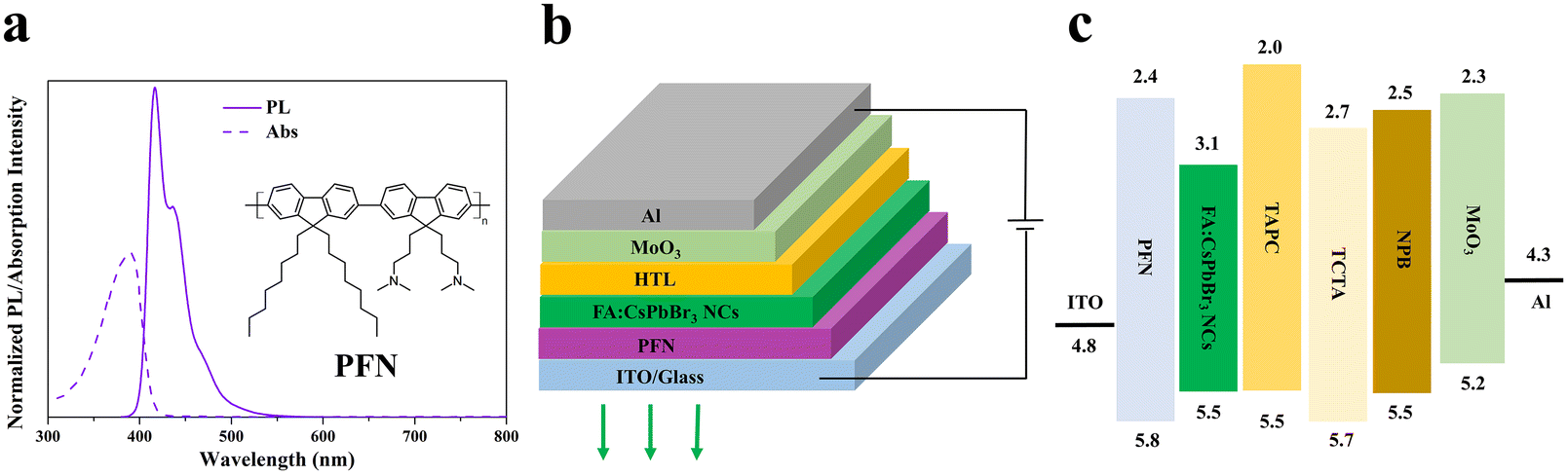 | ||
| Fig. 1 (a) The chemical structure, PL and absorption spectra of PFN. (b) The device structure of inverted LEDs. (c) The material energy levels used in the inverted LEDs. | ||
Due to their excellent performances and ease of synthesis, FA:CsPbBr3 NCs were chose here as the emission layer and synthesized through a triple-ligand room-temperature method according to the previous work.1 A series of characterizations of FA:CsPbBr3 NCs, including transmission electron microscopy (TEM) images, size distribution, X-ray diffraction (XRD) pattern, absorption spectrum and photoluminescence (PL) spectrum, were carried out and are shown in ESI (Fig. S1–S3†). It can be seen that the monodispersed FA:CsPbBr3 NCs belong to a cubic phase with an average size of 11.45 nm. The narrow PL spectrum of the FA:CsPbBr3 NCs corresponds to an excitonic emission with the maximum peak at 512 nm, and a narrow full width at half maximum (FWHM) of 22 nm. The PLQY of the PNCs in octane solution is over 85%. These results indicate that FA:CsPbBr3 NCs will be a suitable emission material in LED device.
As mentioned above, compared to PEDOT:PSS, PFN is more chemically inert. To see if PFN can be a good ETL in the PNC-LED devices, we then proceeded with experimentally validating the potential of the PFN layer by fabricating and testing opaque inverted devices with the architecture shown in Fig. 1b embedding a layer of the PNCs emissive layer. PFN layers with different thicknesses were deposited on the clear pattern indium-doped tin oxide glass (ITO/Glass) substrates by spin-coating PFN solution (in methyl alcohol) with different concentrations (0.1 mg ml−1, 0.5 mg ml−1, 1.0 mg ml−1 and 1.5 mg ml−1). Tris(4-carbazoyl-9-ylphenyl)amine (TCTA) was used as HTL. The performance results are shown in Fig. 2 and Table 1. For easy identification, these inverted devices are named according to the PFN solution concentration, such as PFN-0.1 (fabricated with 0.1 mg ml−1 PFN solution).
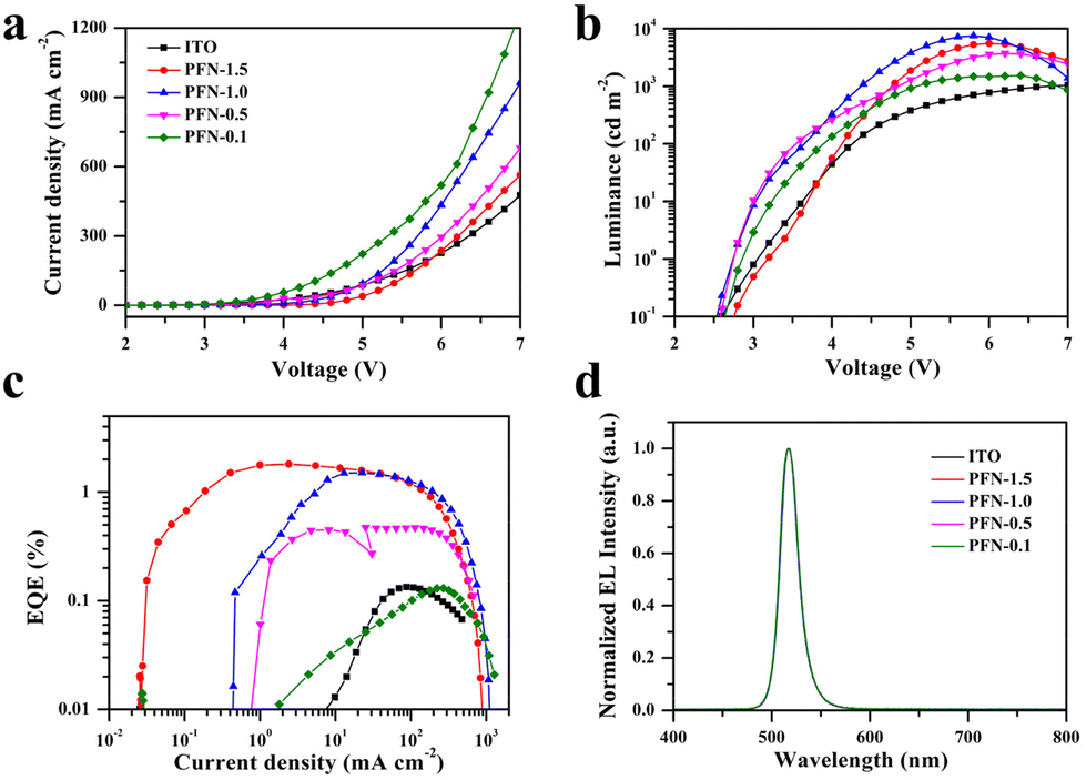 | ||
| Fig. 2 The performance of inverted LED devices with different PFN layer thicknesses: (a) current density–voltage curves, (b) luminance–voltage curves, (c) current density–EQE curves and (d) EL spectra of the devices. | ||
| ETL | V T (V) | L max (cd m−2) | CEmax (cd A−1) | EQEmax (%) |
|---|---|---|---|---|
| without PFN | 3.2 | 1041 | 0.43 | 0.13 |
| PFN-0.1 | 3.0 | 1526 | 0.42 | 0.13 |
| PFN-0.5 | 2.8 | 3702 | 1.50 | 0.47 |
| PFN-1.0 | 2.8 | 7502 | 4.82 | 1.51 |
| PFN-1.5 | 3.2 | 5533 | 5.79 | 1.82 |
As shown in Fig. 2b and Table 1, when the thickness of the PFN layer increases, the turn-on voltage (VT) decreases first and then increases. It indicates that a suitable thickness of the PFN layer can favor the injection of electrons. However, when the PFN layer is too thick, it blocks the charge transfer and makes the series resistance in the internal device become bigger. For the luminance, compared with the device without PFN as ETL, the devices with PFN as ETL all demonstrate higher luminance. The corresponding maximum EQE (EQEmax) or current efficiency (CEmax) of the device also increases when the PFN layer thickness increases. Compared with the EQEmax of the device without PFN as ETL, that of the device with PFN-1.5 as ETL improves from 0.13% to 1.82%, which is a improvement of over 10-fold. The maximum luminance (Lmax) also increased from 1041 cd m−2 to 5533 cd m−2. It is interesting that the performance between the device without PFN as ETL and the device with PFN-0.1 as ETL are similar, which indicates that the PFN film is too thin to optimize the interface between ITO and the PFN layer. To make sure there is no parasitic emission of PFN in the devices, the electroluminescence (EL) spectra of all devices were also measured and are shown in Fig. 2d. All of the devices emit pure green light and the EL spectral curves overlap well. The peak emission wavelength and FWHM are 517 nm and 21 nm, respectively, which could demonstrate a saturated green color. On the whole, the device with PFN-1.0 as ETL exhibits a low VT and relatively high brightness and EQEmax.
To find the reason why the PFN could improve the performance of the device, the superficial roughness of the bare ITO film and PFN-1.0 film were measured first through an atomic force microscope (AFM). The results are shown in Fig. 3a and b, respectively. It was found that the roughness of the film surface decreased from 3.14 nm (or 2.71 nm for 1 μm) to 2.21 nm (or 1.74 nm for 1 μm), which means the PFN film has a smoother surface that helps the charge transport in the device. The PL decay of the FA:CsPbBr3 NCs on different substrates were also measured, and are shown in Fig. 3c and Table S1.† It can be seen that the average lifetime increases after the PFN layer is inset between ITO and the PNC layer. When the PFN layer is thicker, the average lifetime of the PL decay will be longer. Compared with the film without PFN (ITO/FA:CsPbBr3 NCs), the average lifetime of the film with PFN-1.0 as the inset layer (ITO/PFN-1.0/FA:CsPbBr3 NCs) improves from 19.58 ns to 33.04 ns. It seems that the PFN inset layer avoids the fluorescence quenching between ITO and the emission layer. The amine group of PFN also passives the defects of FA:CsPbBr3 NCs, which improves the PLQY of the emission film. As shown in the inset in Fig. 3c, the FA:CsPbBr3 NC film on the ITO/PFN-1.0 substrate demonstrates higher brightness than the film on the bare ITO substrate under UV light.
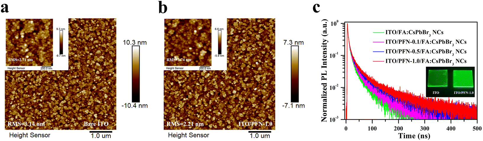 | ||
| Fig. 3 The AFM images of FA:CsPbBr3 NC film on (a) bare ITO and (b) ITO/PFN-1.0. (c) The PL decay curves for FA:CsPbBr3 NCs fabricated on different substrates. The inset is the photograph of the FA:CsPbBr3 NCs films on bare ITO or ITO/PFN-1.0 substrates under UV light. | ||
To investigate the influence of HTL on the device performance, two other p-type organic materials di-[4-(N,N-ditolyl-amino)-phenyl]cyclohexane (TAPC) and N,N′-di(naphthalene-1-yl)-N,N′-diphenyl-benzidine (NPB) were selected and evaporated during the LED fabrication process. The EL spectra of the three devices were measured first. The results (as shown in Fig. 4d) indicate that there is no parasitic emission from PFN. Although TPAC and NPB have similar HOMO values,25,26 the VT of the PNC-LED device clearly decreases from 3.0 eV to 2.6 eV (Table 2) when the HTL changes from TPAC to NPB, which may due to their hole mobility difference. The hole mobility of TPAC is ∼1.0 × 10⁻² m2 V−1 s−1,25,27 which is 7 orders of magnitude higher than the electron mobility of PFN (∼3.0 × 10⁻⁹ m2 V−1 s−1 (ref. 28)). The hole mobility of NPB is ∼1.63 × 10⁻⁵ m2 V−1 s−1. Thus, the balance of charge transport in the devices with NPB as HTL is better, which helps to decrease the VT and improve the luminance. It should also be noted that the hole mobility of TCTA (∼2.0 × 10⁻⁵ m2 V−1 s−1 (ref. 29)) is similar to that of NPB, but the corresponding LED device performance is lower than that of the device based on NPB as HTL. It should be attributed to the relatively higher energy barrier between HTL and the emission layer, as shown in Fig. 1c.
| HTL | V T (V) | L max (cd m−2) | CEmax (cd A−1) | EQEmax (%) |
|---|---|---|---|---|
| TAPC | 3.0 | 5754 | 3.84 | 1.20 |
| TCTA | 2.8 | 7502 | 4.82 | 1.51 |
| NPB | 2.6 | 12540 |
6.72 | 2.07 |
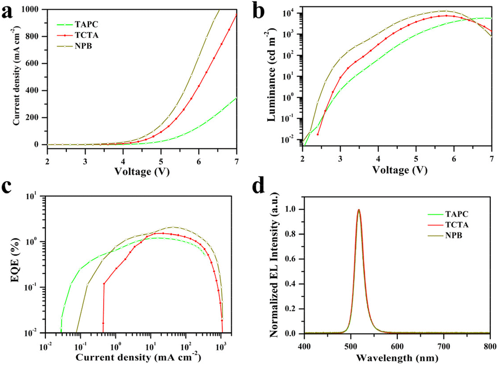 | ||
| Fig. 4 The performance of inverted LED devices with different HTL: (a) current density–voltage curves, (b) luminance–voltage curves, (c) current density–EQE curves and (d) EL spectra of devices. | ||
Based on the above results, we fabricated semitransparent PNC-LEDs with PFN as ETL and NPB as HTL, together with MoO3/Au/MoO3 as the top electrode (Fig. 5a). The performance of the semitransparent LED device is shown in Fig. 5. It is exciting that the EL spectral curves from both top side and bottom side overlap well (Fig. 5b), which means that the transparent top electrode does not influence the emission feature. It also can be seen that the current density–voltage curves are consistent in the whole (Fig. 5d), especially among the low voltage range. The curve difference in the high voltage region may be attributed to damage to the device due to the Joule heating. Due to the different luminance emitted from the top or bottom side under the same voltage (Fig. 5e), the EQE values are slightly different (Fig. 5f). The parameters of the performance are listed in Table 3. Both top and bottom sides show a low VT (2.6 eV) and high brightness (over 1600 cd m−2), together with similar maximum EQE values of about 0.4%. Although this performance is not as good as the PNC-LED with a forward structure,16,18,30 it is one of the best performances among the PNC-LEDs with an inverted structure.17 The transmittance of the device between 420 and 800 nm is over 50%, with 67% around 520 nm. Compared with the transmittance of ITO, the PFN layer almost has no effect on the device transmittance. The transmittance loss results from other functional layers. For instance, the transmittance loss around 500 nm should be attributed to the absorption of FA:CsPbBr3 NCs (as shown in Fig. S3†). It is exciting that it is easy to see the logo through the semitransparent PNC-LED device, as shown in Fig. 5c, which indicates the potential application in transparent display products.
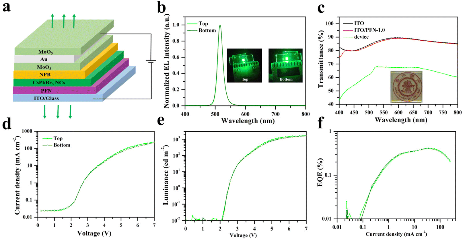 | ||
| Fig. 5 The device structure and performance of the semitransparent inverted LEDs devices. (a) Semitransparent LED device structure. (b) The photographs of the semitransparent LED device. (c) The transmittance of ITO (black), ITO-PFN-1.0 (red) and semitransparent device (green). The inset is the photograph of a device with the same structure as the inverted semitransparent PNC-LED device. (d) Current–voltage curves. (e) Luminance–voltage curves. (f) EQE–current density curves. | ||
| Electrode | V T (V) | L max (cd m−2) | CEmax (cd A−1) | EQEmax (%) |
|---|---|---|---|---|
| Top (MoO3/Au/MoO3) | 2.6 | 1643 | 1.34 | 0.40 |
| Bottom (ITO) | 2.6 | 1619 | 1.31 | 0.41 |
4. Conclusion
In summary, we successfully demonstrate the opaque and semitransparent green LEDs with PFN and FA:CsPbBr3 PNCs as ETL and emission layer, respectively. Through the optimization of the thickness of the PFN layer and changing the HTL material, we achieved the maximum EQE and luminance of the opaque LEDs at over 2% and 12000 cd m−2, respectively. For the semitransparent PNC-LED device, the total emission achieved a peak luminance of 3262 cd m−2. In addition, the average transmittance is over 61% in the visible region. Our study demonstrates the potential application of PNCs for transparent display.
Author contributions
Qun Wan: designed the experiment, performed the experiment and wrote the manuscript; Qinggang Zhang and Jinlong Guo: assisted with the experiments, and prepared figures and tables. Mingming Liu, Wenji Zhan, Xinrong Liao, Changwei Yuan, Mengda He, Weilin Zheng, Congyang Zhang and Long Kong: polished the English language, analyzed the data, and revised the manuscript. Liang Li: corresponding author, critical revision of article, final approval of the article.Conflicts of interest
There are no conflicts of interest to declare.Acknowledgements
This work was supported by the National Natural Science Foundation of China (NSFC 22175113, 42007125, 22205136), Start-up Founding for Scientific Research from Macau University of Science and Technology (SSF-22-001-MIMSE), the China Postdoctoral Science Foundation (2021M702115); Shanghai Post-doctoral Excellence Program (2021239); and Joint Funds of the National Natural Science Foundation of China (No. U21A20320).References
- J. Song, J. Li, L. Xu, J. Li, F. Zhang, B. Han, Q. Shan and H. Zeng, Adv. Mater., 2018, 30, e1800764 CrossRef PubMed.
- B. Wang, C. Zhang, W. Zheng, Q. Zhang, Q. Wan, L. Kong and L. Li, Chem. Commun., 2020, 56, 11291–11294 RSC.
- W. Zheng, Q. Wan, Q. Zhang, M. Liu, C. Zhang, B. Wang, L. Kong and L. Li, Nanoscale, 2020, 12, 8711–8719 RSC.
- M. He, Q. Zhang, F. Carulli, A. Erroi, W. Wei, L. Kong, C. Yuan, Q. Wan, M. Liu, X. Liao, W. Zhan, L. Han, X. Guo, S. Brovelli and L. Li, ACS Energy Lett., 2023, 8, 151–158 CrossRef CAS.
- J. Song, J. Li, X. Li, L. Xu, Y. Dong and H. Zeng, Adv. Mater., 2015, 27, 7162–7167 CrossRef CAS PubMed.
- T. Chiba, Y. Hayashi, H. Ebe, K. Hoshi, J. Sato, S. Sato, Y.-J. Pu, S. Ohisa and J. Kido, Nat. Photonics, 2018, 12, 681–687 CrossRef CAS.
- Y. Dong, Y. K. Wang, F. Yuan, A. Johnston, Y. Liu, D. Ma, M. J. Choi, B. Chen, M. Chekini, S. W. Baek, L. K. Sagar, J. Fan, Y. Hou, M. Wu, S. Lee, B. Sun, S. Hoogland, R. Quintero-Bermudez, H. Ebe, P. Todorovic, F. Dinic, P. Li, H. T. Kung, M. I. Saidaminov, E. Kumacheva, E. Spiecker, L. S. Liao, O. Voznyy, Z. H. Lu and E. H. Sargent, Nat. Nanotechnol., 2020, 15, 668–674 CrossRef CAS PubMed.
- Y.-H. Kim, S. Kim, A. Kakekhani, J. Park, J. Park, Y.-H. Lee, H. Xu, S. Nagane, R. B. Wexler, D.-H. Kim, S. H. Jo, L. Martínez-Sarti, P. Tan, A. Sadhanala, G.-S. Park, Y.-W. Kim, B. Hu, H. J. Bolink, S. Yoo, R. H. Friend, A. M. Rappe and T.-W. Lee, Nat. Photonics, 2021, 15, 148–155 CrossRef CAS.
- L. Liu, K. Cao, S. Chen and W. Huang, Adv. Opt. Mater., 2020, 8, 2001122 CrossRef CAS.
- J. K. Song, D. Son, J. Kim, Y. J. Yoo, G. J. Lee, L. Wang, M. K. Choi, J. Yang, M. Lee, K. Do, J. H. Koo, N. Lu, J. H. Kim, T. Hyeon, Y. M. Song and D. H. Kim, Adv. Funct. Mater., 2016, 27, 1605286 CrossRef.
- M. S. White, M. Kaltenbrunner, E. D. Głowacki, K. Gutnichenko, G. Kettlgruber, I. Graz, S. Aazou, C. Ulbricht, D. A. M. Egbe, M. C. Miron, Z. Major, M. C. Scharber, T. Sekitani, T. Someya, S. Bauer and N. S. Sariciftci, Nat. Photonics, 2013, 7, 811–816 CrossRef CAS.
- G. Huseynova, J. H. Lee, Y. H. Kim and J. Lee, Adv. Opt. Mater., 2021, 9, 2002040 CrossRef CAS.
- C. W. Hsu, B. Zhen, W. Qiu, O. Shapira, B. G. DeLacy, J. D. Joannopoulos and M. Soljacic, Nat. Commun., 2014, 5, 3152 CrossRef PubMed.
- X. Dai, Y. Deng, X. Peng and Y. Jin, Adv. Mater., 2017, 29, 1607022 CrossRef PubMed.
- Q. Shan, J. Song, Y. Zou, J. Li, L. Xu, J. Xue, Y. Dong, B. Han, J. Chen and H. Zeng, Small, 2017, 13, 1701770 CrossRef.
- C. Xie, X. Zhao, E. W. Y. Ong and Z. K. Tan, Nat. Commun., 2020, 11, 4213 CrossRef CAS PubMed.
- H. Wu, Y. Zhang, X. Zhang, M. Lu, C. Sun, X. Bai, T. Zhang, G. Sun and W. W. Yu, Adv. Electron. Mater., 2018, 4, 1700285 CrossRef PubMed.
- J. Liang, X. Guo, L. Song, J. Lin, Y. Hu, N. Zhang and X. Liu, Appl. Phys. Lett., 2017, 111, 213301 CrossRef.
- J. Kwak, W. K. Bae, D. Lee, I. Park, J. Lim, M. Park, H. Cho, H. Woo, D. Y. Yoon, K. Char, S. Lee and C. Lee, Nano Lett., 2012, 12, 2362–2366 CrossRef CAS PubMed.
- D. Kim, Y. Fu, S. Kim, W. Lee, K.-H. Lee, H. K. Chung, H.-J. Lee, H. Yang and H. Chae, ACS Nano, 2017, 11, 1982–1990 CrossRef CAS PubMed.
- K. M. Reza, S. Mabrouk and Q. Qiao, Proc. Nat. Res. Soc., 2018, 2, 02004 CrossRef.
- D. A. Mengistie, M. A. Ibrahem, P. C. Wang and C. W. Chu, ACS Appl. Mater. Interfaces, 2014, 6, 2292–2299 CrossRef CAS PubMed.
- C. Feng, X. Wang, Z. He and Y. Cao, Sol. RRL, 2021, 5, 2000753 CrossRef CAS.
- S. Zhong, R. Wang, H. Y. Mao, Z. He, H. Wu, W. Chen and Y. Cao, J. Appl. Phys., 2013, 114, 113709 CrossRef.
- J.-H. Jou, P.-H. Wu, C.-H. Lin, M.-H. Wu, Y.-C. Chou, H.-C. Wang and S.-M. Shen, J. Mater. Chem., 2010, 20, 8464 RSC.
- Y. Hamada, H. Kanno, T. Tsujioka, H. Takahashi and T. Usuki, Appl. Phys. Lett., 1999, 75, 1682 CrossRef CAS.
- R. A. K. Yadav, D. K. Dubey, S. Z. Chen, T. W. Liang and J. H. Jou, Sci. Rep., 2020, 10, 9915 CrossRef CAS.
- C. Han, Y. Cheng, L. Chen, L. Qian, Z. Yang, W. Xue, T. Zhang, Y. Yang and W. Cao, ACS Appl. Mater. Interfaces, 2016, 8, 3301–3307 CrossRef CAS.
- D.-H. Lee, Y.-P. Liu, K.-H. Lee, H. Chae and S. M. Cho, Org. Electron., 2010, 11, 427–433 CrossRef CAS.
- Q. Wan, L. Huang, L. Kong, Q. Zhang, C. Zhang, M. Liu, X. Liao, W. Zhan, W. Zheng, C. Yuan, M. He and L. Li, ACS Appl. Mater. Interfaces, 2022, 14, 19697–19703 CrossRef CAS PubMed.
Footnote |
| † Electronic supplementary information (ESI) available. See DOI: https://doi.org/10.1039/d2nr06998a |
| This journal is © The Royal Society of Chemistry 2023 |