
Hybrid 2D perovskite and red emitting carbon dot composite for improved stability and efficiency of LEDs†
Amandeep Singh
Pannu‡
 *abd,
Suvankar
Sen‡§
a,
Xiaodong (Tony)
Wang
bc,
Robert
Jones
bc,
Kostya (Ken)
Ostrikov
ab and
Prashant
Sonar
*ab
*abd,
Suvankar
Sen‡§
a,
Xiaodong (Tony)
Wang
bc,
Robert
Jones
bc,
Kostya (Ken)
Ostrikov
ab and
Prashant
Sonar
*ab
aSchool of Chemistry and Physics, Faculty of Science, Queensland University of Technology, Brisbane, QLD 4001, Australia. E-mail: sonar.prashant@qut.edu.au; a.pannu@qut.edu.au; a.pannu@griffith.edu.au
bCentre for Materials Science, Queensland University of Technology, Brisbane, QLD 4001, Australia
cCentral Analytical Research Facility, Queensland University of Technology, Brisbane, Australia
dQueensland Micro- and Nanotechnology Centre (QMNC), Griffith University, Nathan Campus, Nathan, QLD 4111, Australia
First published on 9th January 2023
Abstract
Organic–inorganic hybrid lead trihalide perovskites have shown promise consistently in optoelectronic devices such as light-emitting diodes (LEDs), solar cells, photodetectors, sensors, and other optoelectronic devices. Perovskite-based LEDs (PSK-LEDs) have shown enormous potential, mostly due to their lower cost, easy synthesis via solution processibility, and highly tunable light-emitting behavior with higher performance. Despite the recent developments in green and blue PSK-LEDs over the years, there has been less development in the research area of red-emitting PSK-LEDs. Although some developments have led to spectrally, stable red-emitting PSK-LEDs, the stability of those devices still needs to be improved upon further for any practical application. In this work, to the best of our knowledge, for the first time, we used red-emitting 2D PSK as an active light-emitting layer which was further stabilized by red-emitting carbon dots (CDs). The CD-PSK composite films were used as an active layer in red emitting LEDs, and they showed high operational stability, and improved performance compared to the control device with only PSK film as the active layer. The composite device showed improved maximum luminescence (3011 cd m−2), charge density (330 mA cm−2), operational stability (8 hours), better EQE (10.2%), and low turn-on voltage of 2.6 V compared to the control device with maximum luminescence (1512 cd m−2), charge density (134 mA cm−2), operational stability (<2 hours), EQE (2.6%) and turn on voltage of 3.2 V. The low-cost hybrid approach using PSK building blocks together with CDs opens a new approach leading to a composite material, which has immense possibilities for tuning the structure further to maximize the performance.
Introduction
Hybrid organic–inorganic perovskites have emerged as a promising class of next-generation optoelectronic materials in a diverse array of photonic and electronic device applications. In the domain of light-emitting devices, organic–inorganic hybrid perovskites have emerged as a highly competitive counterpart to the traditional either purely organic or inorganic semiconductors in terms of production cost, ease of material synthesis as in low-temperature solution processing, wide color gamut, high color purity, good charge transport properties, flexible bandgap tuning, among others.1 It was in 2014 when the first instance of room-temperature electro-luminescence was observed from perovskite-based LEDs (PSK-LEDs). Since then, massive strides have been made to synthesize a variety of perovskite nanocrystals, quantum dots, etc. to varying degrees of success. In most cases, metal halide PSK-LEDs have been successfully designed to emit in the green region of the visible spectrum, by making use of methylammonium lead bromide (MAPbBr3), cesium lead bromide (CsPbBr3), or surface treatment of inorganic CsPbI3.2–4 Some successes have been found in the case of blue color emission as well by using CsPbI3. For a wide gamut of color displays along with solid-state lighting applications, the additive mixing of red, green, and blue is necessary for purposes of commercialization. To address this issue, high-quality perovskites need to be synthesized with the desired optical and electronic properties. Among the three, the red color has been challenging to obtain and sustain with effectiveness. For designing efficient and long-lasting LEDs by using CsPbX3 type of perovskites, some of the desirable features include a lower band gap, larger absorption spectrum, with acceptable color purity which can be replicated.5 With perovskite-based devices though, the chief concerns are the lower stability and poor device efficiency. The issues become exaggerated with the red-emitting PSKs, for instance in the case of CsPbI3, where its phase undergoes transitions under ambient conditions.6 The red color LEDs have a wide range of applications as well as it is crucial for fabricating white LEDs. Different attempts have been made to synthesize good-performing perovskite red emitters and the two most promising approaches are (i) varying the halide compositions and (ii) systematically tuning the quantum well structures. Over the past few years, quasi-2D perovskites7,8 is pushing the limit of the operational stability and photostability of LEDs based on such materials. The primary reason for this new shift towards the lower-dimensional counterparts of the 3D PSKs is to offset the drawbacks suffered by 3D PSKs under ambient conditions which predominantly include moisture, temperature, and light. This results in the PSK structure becoming unstable and degrading to its components, which drastically reduces the effectiveness of the device. These, in turn, reduce the scope of practical utility and commercialization of 3D PSK-based LEDs and other devices. In perovskites, the general interactions exist between A-site cations and corner-sharing octahedra [BX6]4− respectively. This coordination between the A-site cation and the corner octahedra determines the dimensionality of the perovskite.9,10 Structurally, 3D PSKs can be converted to lower dimensions by completely or partially replacing small A-site cations with other bulky organic cations (including two-dimensional (2D), one-dimensional (1D), and zero-dimensional (0D) perovskites. It's worth noting that the low dimensionality mentioned here means that each component of the perovskite has at least one dimension to the extent of molecular level and has nothing to do with the final morphology of the perovskite, for instance, nanosheets, nanowires, nanocrystals, etc. Unlike 3D perovskite, however, the large hydrophobic spacer cations of low-dimensional perovskite can effectively improve thermal stability and reduce water penetration.11–13Recently, a novel approach was introduced by Amandeep Singh Pannu et al.8,9 and in that work, they systematically used low-cost carbon dots (CDs) processed from human hair as the bio-waste for the improvement of the operational stability of the light emitting display devices as well as light-harvesting solar cell devices by capping active layer with the CD layer and improved the overall stability. The CDs have active hydroxyl or carboxylic acid groups so their surfaces can be functionalized systematically by surface passivation. Such passivation not only allows higher stability to the devices but also provides an opportunity to tune the energy levels as well as assist performance enhancement. Due to the easy tuning of the surface of CDs, they are promising quantum dot candidates to tune the PSK material and device characteristics. As per our knowledge, the current work is the first such kind of effort to improve the operational stability of 2D PSK using CDs, which have a common red emission region without hampering optical change.
Herein, we demonstrate that 2D PSK and CDs together as the composite approach to improving the stability of the PSK material used as active light emitting layer in display devices. Two building blocks, red-emitting CDs and quasi-2D perovskite (PSK) were initially synthesized. The building material was used to fabricate composite material thin films for fabricating devices. The CDs play a dual role in protecting the perovskite material from degradation and it also reduces the band offset, which is needed for effective charge injection in LED device structure. The PSK (control) and CD-PSK (composite) were used as active layers to fabricate the LED devices. The composite device exhibits improved max luminescence of 3011 cd m−2, a charge density of 330 mA cm−2, better external quantum efficiency (EQE) of 10.2%, operational stability of 8 hours, and low turn-on voltage of 2.6 V compared to the control device (where only 2D PSK used as an active emitting layer) with max luminescence of 1512 cd m−2, charge density 134 mA cm−2, operational stability (<2 hours), EQE of 2.6% and turn-on voltage of 3.2 V.
Synthesis of hybrid material
To prepare the control sample of perovskite (PSK), initially Cesium Iodide (CsI) and Lead Iodide (PbI2) 0.35 molar solution in Dimethyl Sulfoxide (DMSO) were prepared. The solution was then filtered through a 0.45 μm filter, and afterward, organic salt Benzyl Ammonium Iodide (BAI) was added to the above solution in equal molar concentration (write molarity value). To obtain is (BA)2(Cs)n−1PbnI3n+1 quasi-2D perovskite (PSK) control sample.7 Afterward, an equal volume of Poly (Ethylene Oxide) (PEO) with a concentration of 10 mg ml−1 in DMSO was mixed with the above solution and spin-coated at 4000 rpm for 30 s on the given substrate. Here, BA refers to Benzylammonium (C7H10N+), Cs is Cesium (Cs+), Pb is Lead ion (Pb2+) and I is Iodide (I−). The concentration of CDs was adjusted to control the number of layers. Each step of the synthesis process is depicted in Fig. 1.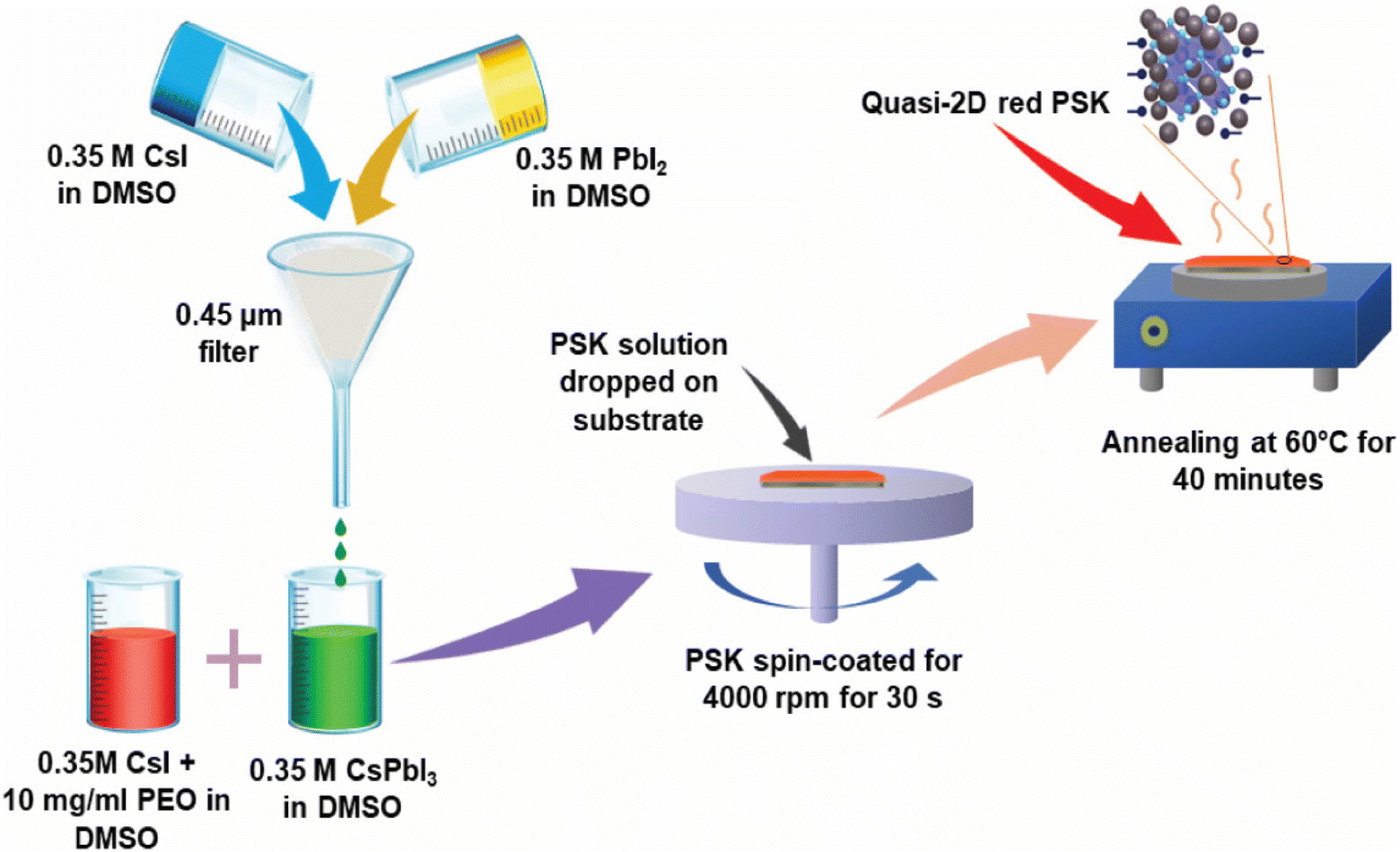 | ||
| Fig. 1 Step-by-step depiction of synthesis of the red-emitting PSK control sample. | ||
Synthesis of red-emitting CDs
A stock solution of 1.5 mg citric acid with 2.6 mL of ethylenediamine in 100 mL of formamide solution was made. 10 mL of this solution was transferred in a glass vial for microwave reaction. The solution was heated at 180 °C for 4 hours at constant pressure. The final mixture was cool down to room temperature and precipitated with excess acetone and centrifuged at 10![[thin space (1/6-em)]](https://www.rsc.org/images/entities/char_2009.gif) 000 rpm for 5 min. Multiple centrifuge washing was done to extract the final product and dried it in a vacuum oven. The final product was resuspended in DMSO and the whole solution was filtered by a 0.22 μm syringe filter.
000 rpm for 5 min. Multiple centrifuge washing was done to extract the final product and dried it in a vacuum oven. The final product was resuspended in DMSO and the whole solution was filtered by a 0.22 μm syringe filter.
The number of layers of PSK can be roughly estimated from d001 spacing according to formula10
| d001 = a × n + x |
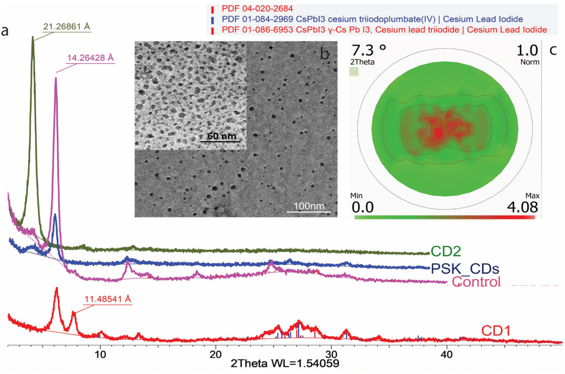 | ||
| Fig. 2 (a) Grazing angle diffraction (GID) of a thin film of a different composite of PSK and CDs with various thicknesses. (b) TEM image of 2D perovskite (PSK), inset showing the image at higher resolution, and (c) XRD texture measurement of the composite thin film. | ||
The spin-coated thin films were annealed at 60 °C to form the final PSK 2D control sample. Fig. 2b shows the TEM of 2D PSK crystals. The TEM of the film was obtained by pressing the film onto the carbon-coated copper grids for TEM. The optimum temperature for processing the films was determined from in situ XRD studies. The in situ XRD data of 2D layer perovskite crystals with respect to temperature is shown in (Fig. S1†). The precursor was initially amorphous until a low angle peak at 23.7 Å and a peak at 6.8 Å emerged from 50 °C. As the temperature kept increasing, these peaks disappeared above 80 °C while the cubic phase 100 peak at 6.3 Å and 200 peaks at 3.15 Å started to form as low as 70 °C. Between 70 °C to ∼110 °C, only the cubic phase of CsPbI3 (PDF# 01-080-4039) exists, which gradually turned into an orthorhombic phase of CsPbI3 (PDF# 04-016-5078) from 105 °C. To reveal the PSK grain orientations in the heat-synthesized PSK_CDs sample, the pole figure of the 001 reflection (14.26 Å) was measured using a Bruker D8 Advance X-ray Diffractometer (Fig. 2c).
It is evident from Fig. 2c, that the 001-crystal plane is mostly parallel to the sample surface, confirming a 2D hybrid structure.
The CDs not only help to form a pure phase 2D PSK film by sandwiching between the different layers (Fig. 3a) but also increases the hydrophobic nature of the film as evident from contact angle measurements. The contact angle of the control film was measured to be 56.98°, (Fig. 3b) while it increases to 83.09° in the case of PSK and CD3 composite film (PSK_CD) (Fig. 3c).
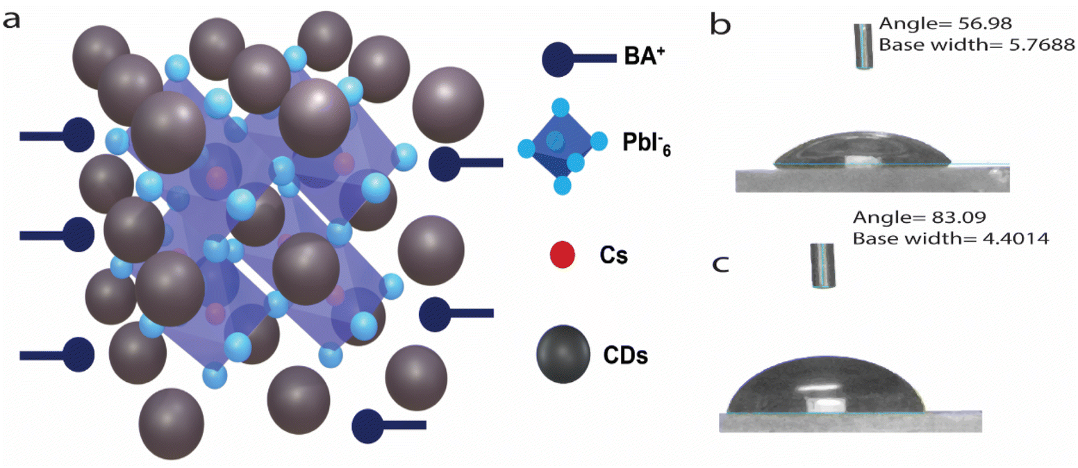 | ||
| Fig. 3 (a) Schematic of PSK and CDs, sandwiched between PSK layers. (b) Thin film contact angle of control PSK film and (c) composite of PSK and CD3. | ||
The CDs used to develop composite film, were optimized to emit in a similar optical region as PSK, and emission was independent of excitation. The excitation-independent emission is due to the absence of shallow defects that can be excited by 500 nm or higher excitation wavelength (Fig. 4a). The CDs were excited between 530 nm to 550 nm, and the photoluminescence (PL) maximum was recorded near 625 nm (Fig. 4a and b). The control and composite material PL were also investigated. The pristine PSK thin film has PL maxima at 650 nm while the composite film emission shifts to 660 nm (Fig. 4c). The incorporation of CDs between the layers of PSK, expanded the lattice for the same n (number of layers), hence shifting the PL emission by 10 nm. The control sample exhibits double absorption peaks in the absorption spectrum (Fig. 4d) however in the case of the PSK-CDs sample the first peak is diminished while the second peak is red-shifted which is in line with the red shift in PL emission. This redshift in absorption may be associated with an increase in average crystal size.
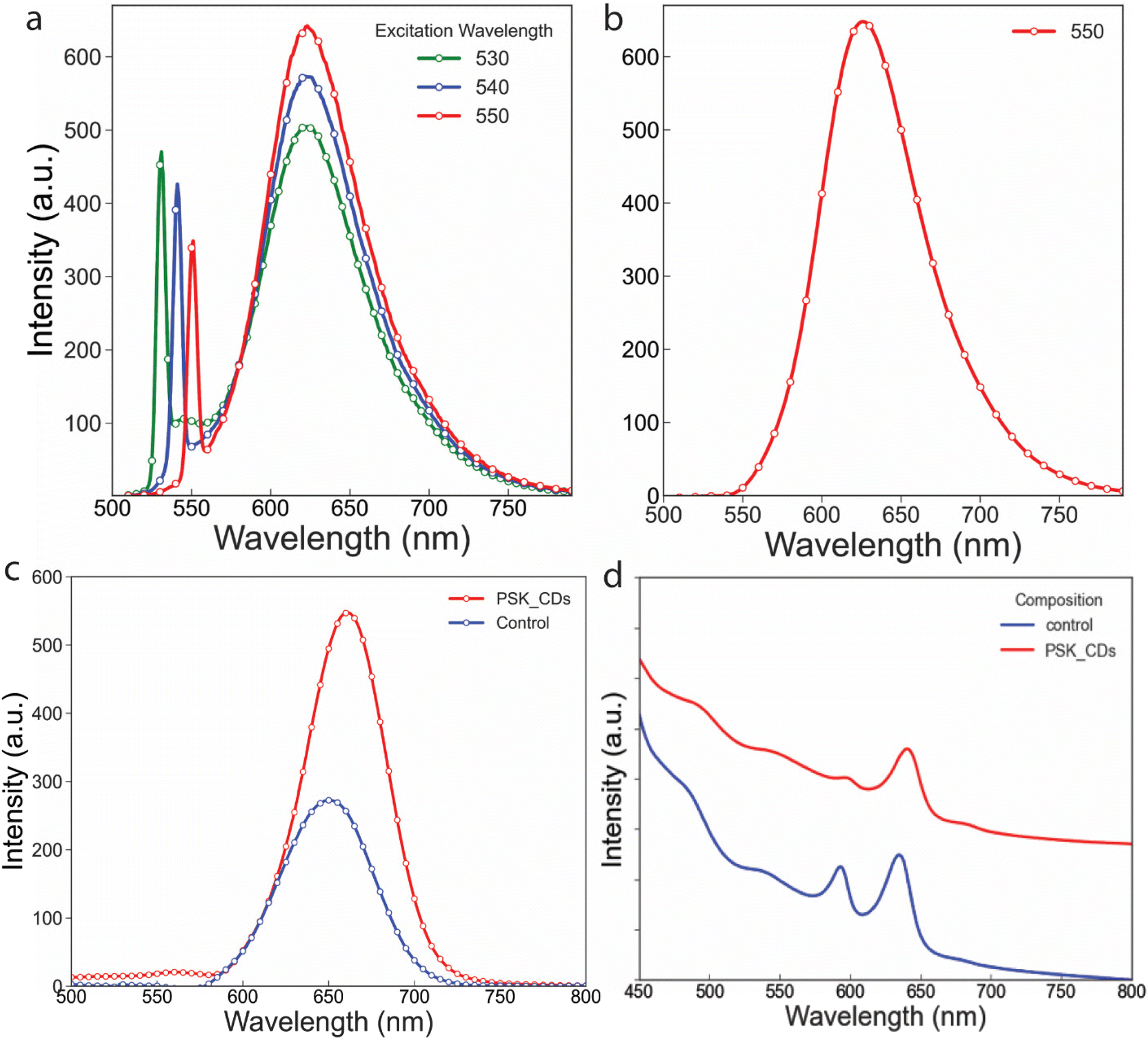 | ||
| Fig. 4 (a) and (b) Photoluminescence (PL) of CDs at the various excitation wavelengths. (c) PL of a thin film of control PSK sample and PSK and CD3 composite. (d) UV-absorption studies of all thin-film samples. | ||
To further investigate the composite stability XPS studies were done on control and composite PSK_CD samples exposed to air. The wide scan XPS (Fig. 5a) indicates the presence of carbon dot as the carbon content in PSK_CD increases to 22.68% from 9.37% in the case of a control sample.
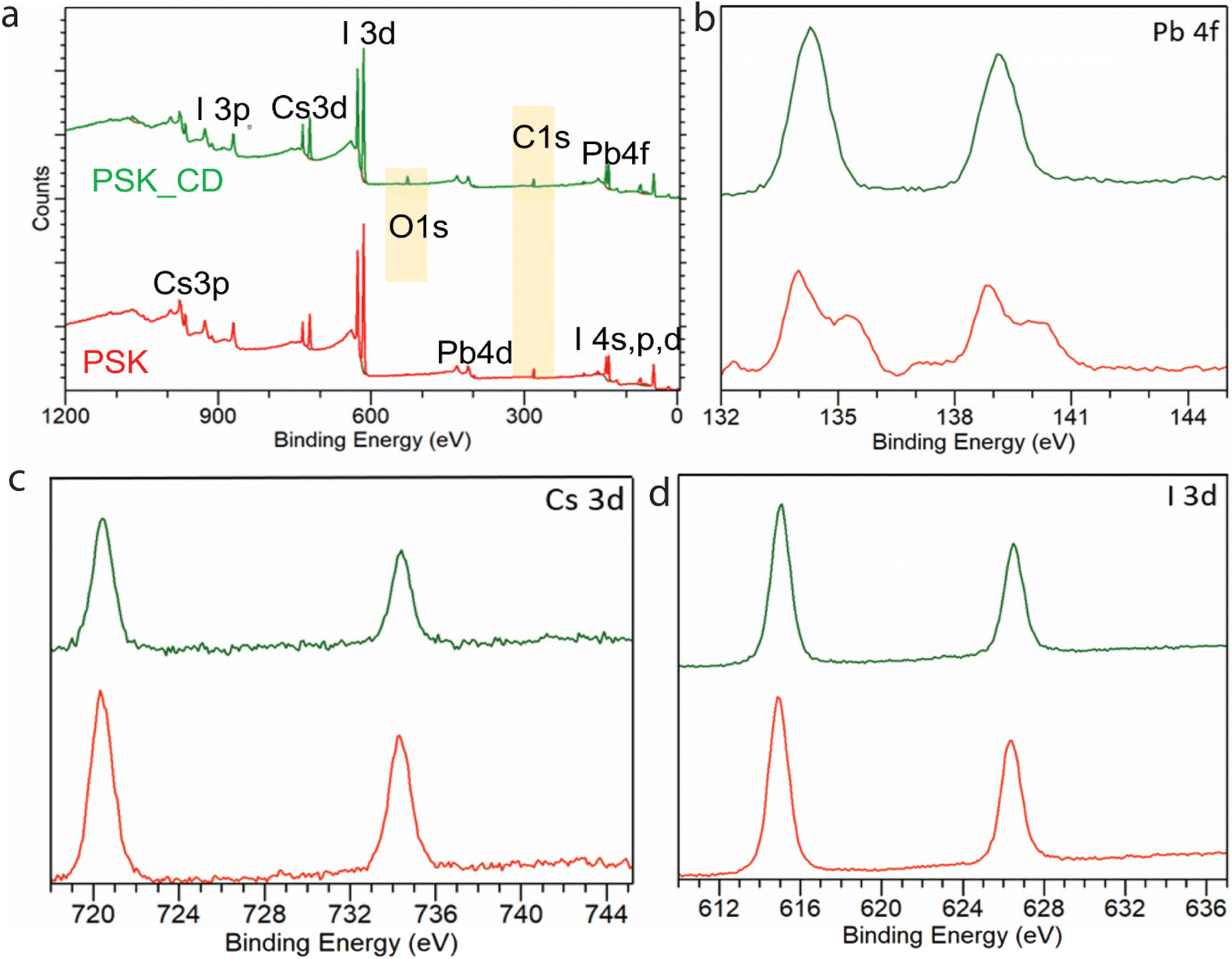 | ||
| Fig. 5 (a) XPS survey spectra of PSK (control, red) and PSK_CD (green). (b) High-resolution Pb4f XPS spectra of PSK and PSK_CD. (c) High-resolution Cs 3d XPS spectra of PSK and PSK_CD. (d) High-resolution I3d XPS spectra of PSK and PSK_CD. | ||
The small amount of oxygen 0.25% adsorbed onto red-emitting CD is also present in wide scan XPS of PSK_CD. The higher resolution scan of Pb 4s of both samples is shown in Fig. 5b. The scan of Pb 4s for control (red) shows peak splitting indicating free lead ions (degradation of sample) compared to composite sample PSK_CD. The CD with hydrophobic properties (clear from the increase in contact angle of composite films) helps to keep the 2D structure of perovskite intact and no free ions are seen in XPS compared to the control sample. The higher resolution scan of Cs 3d (Fig. 5c) and I 3d (Fig. 5d) for both control and PSK_CD does not show any variation, indicating that CDs interact with outer Pb atoms of a unit cell of perovskite. Due to the good structural stability and better optical performance of the composite, the composite thin film was further used as an active emitting layer for fabricating the LED devices. The schematic (Fig. 6a) shows the device structure. The active layer is composed of PSK for the control device and PSK_CD composite for the second device, each 50 nm in thickness. The active layer in devices is sandwiched between poly(3,4-ethylene dioxythiophene)-polystyrene sulfonate (PEDOT: PSS) hole transporting layer (40 nm) deposited on patterned Indium tin oxide (ITO) on the glass substrate and the 2,2′,2′′-(1,3,5-benzinetriyl)-tris(1-phenyl-1-H-benzimidazole), TPBi (50 nm) as the electron transporting layer. The electron was injected with a Lithium Fluoride (LiF) doped silver (Ag) electrode (100 nm) while holes were injected by the ITO electrode. The composite device shows a 4 times improvement of electroluminescence (Fig. 6b) over the control device with stable bias-independent emission around 660 nm. The red-emitting CDs help in reducing the band offset7 and hence higher current efficiency (Fig. 6c) with respect to the same current density was observed in the case of a composite device as compared to the control device. This is also supported by the ultraviolet photoelectron spectrum (UPS) data of red CDs, and the energy band diagram of the device (see ESI Fig. S3†).
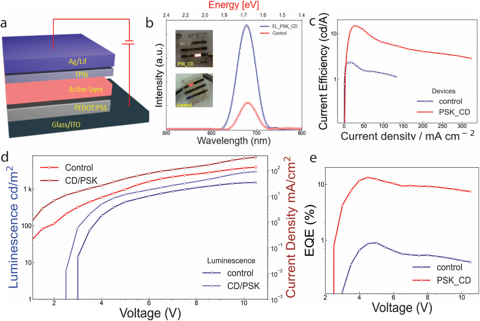 | ||
| Fig. 6 (a) Schematic depicting device structure. (b) EL output spectra of the control device and the composite PSK_CD. Inset: an actual device pixel of control and PSK-CD-based devices under constant bias. (c) Current efficiency versus current density graph for both devices. (d) Luminance–current–voltage (L–I–V) characteristic of control and PSK_CD-based devices. (e) The external quantum efficiency (EQE) of both LEDs vs. applied voltage. | ||
The bandgap energy of red CDS (1.98 eV) is calculated using the equation Eoptg = 1240/λ, where λ is the wavelength corresponding to the highest emission. The energy band diagram for CDs was calculated using UPS and bandgap calculation (Fig. S3a†). The band diagram for the device is shown in Fig. S3b.† It is clear from the band diagram that CDs apart from giving composite structural stability also reduces band offset, hence improving the IVL properties of PSK_CD-based devices compared to the control.
The control device shows maximum luminescence of 1512 cd m−2 with 134 mA cm−2 current density, while the composite-based device due to reduced band offset shows a higher current density of 330 mA cm−2 with maximum luminescence of 3011 cd m−2 (Fig. 6d). With improved charge balance, the composite device shows a very high EQE of 10.2 compared to 2.6 for control devices.
To further investigate the role of CDs in the operational stability of the devices, time-of-flight secondary-ion mass spectrometry (ToF-SIMS) was used to determine chemical differences between damaged and undamaged devices operated over an extended period (10 hours). 3D images acquired from an undamaged CD-PSK device show the 2D structure within the composite layer (Fig. S2a–c† and Fig. 7a). Images acquired from a damaged CD-PSK device show that the 2D structure is no longer retained (Fig. 7b and Fig. S2d–f†), as the structure degrades into ions, leading to the failure of the device. The presence of CDs in the composite not only helps in reducing the band offset for charge injection of holes in the device but also drastically improves the operational stability of the device beyond 8 hours, compared to less than 1 hour for the control device as seen from the time-resolved ToF-SIMS of the composite PSK (Fig. 7c).
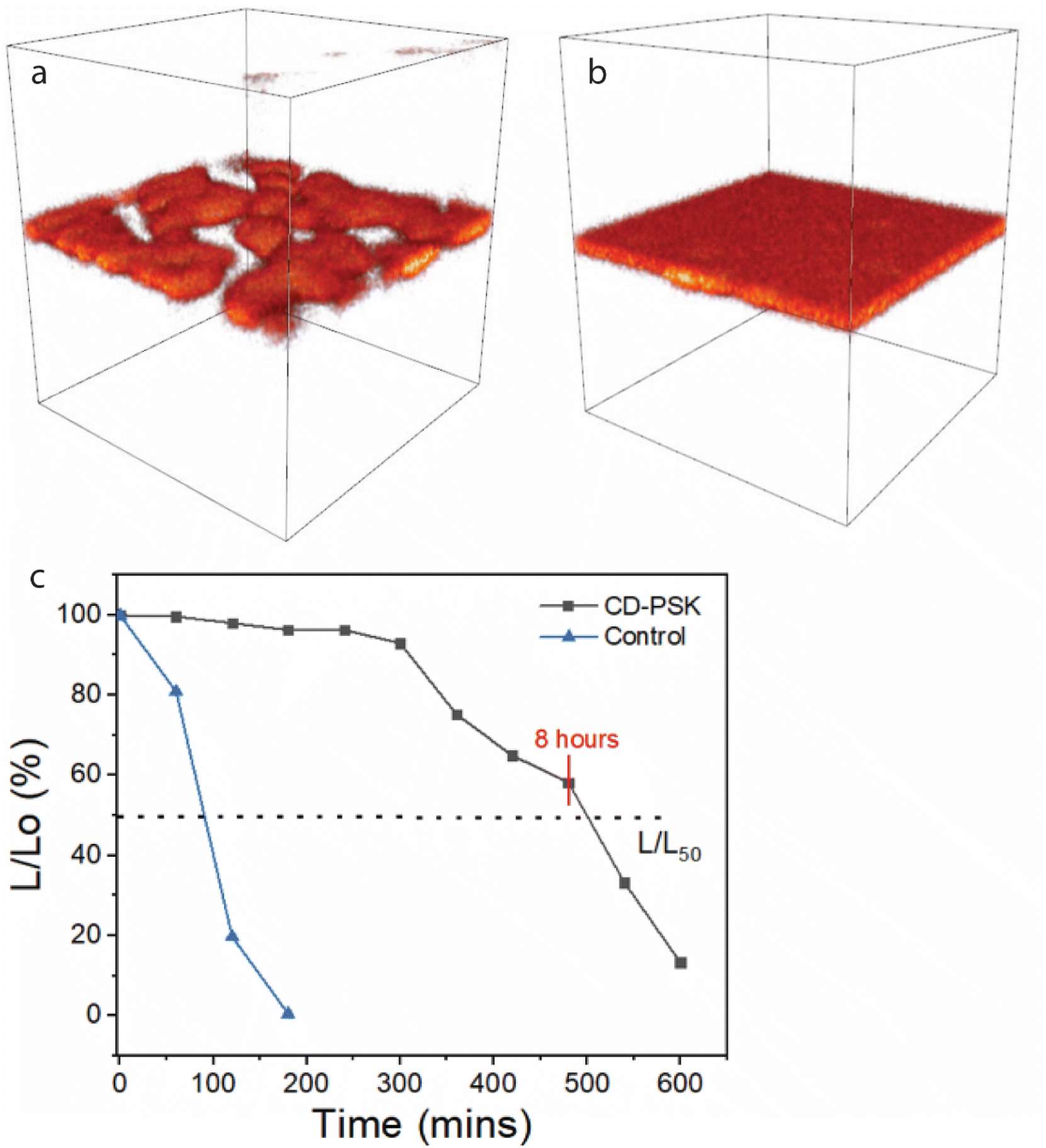 | ||
| Fig. 7 Figures (a) and (b) show 3D renders of the distribution of CsPbI4− ions in the undamaged and damaged devices, respectively, and are oriented so that the upper face in each corresponds to the cap layer, and bottom to the ITO layer. The lengths in the X and Y directions are 200 μm. The Z scale is sputter time. (c) Operational stability of control and CD-PSK device. | ||
Conclusion
In summary, we have successfully synthesized both red-emitting CDs as well as red-emitting 2D PSK as emitting layer building blocks for fabricating hybrid photonic LED devices. Both the building blocks were used to fabricate control (only 2D PSK based) and a composite film (2D PSK + CD based), based LEDs and they were further optimized to get the best device performance. During the optimization of the devices, the parameters such as band offset, and emission control were systematically controlled, and the optimized composite material successfully demonstrate red bright emission. The CD-PSK composite film red emitting LEDs exhibit an improved impressive turn-on voltage of 2.6 V compared to the 3.1 V for the control film of PSK alone. Furthermore, the maximum luminescence of the composite device was 3011 cd m−2 and the current density of 330 mA cm−2 compared to the maximum luminescence of 1512 cd m−2 with 134 mA cm−2 current density of the control device. The improved charge density is attributed to a reduction in band offset and the composite device clearly shows a large increment in operational stability (approx. 8 hours of half lifetime) and EQE of 10.2% compared to the control device with operational stability of fewer than 2 hours and EQE of 2.6%. Our current work of combining two types of photonics quantum dots for the photonic devices represents how the selection and nature of dots are crucial for enhancing performance as well as increasing operation stability. Indeed, this is a promising approach for fabricating future heterostructure quantum dot-based displays and light-harvesting devices and provides a great opportunity to tune the optoelectronic properties systematically via compositional material engineering. There is room to improve the quantum dot material properties further by introducing different ligands for stabilizing hydrophobic CDs and PSK structure synergically and using them for stable device fabrication via moisture-protective layer shielding.Author contributions
Amandeep Singh Pannu: conceptualization, methodology, investigation, writing original draft, formal analysis. Suvankar Sen: conceptualization, investigation and writing original draft. Xiaodong (Tony) Wang: investigation (XRD) and editing draft, Robert Jones: investigation (ToF-SIMS) and editing draft. Kostya (Ken) Ostrikov: resources, reviewing and editing draft, Prashant Sonar: resources, reviewing and editing draft and supervision.Conflicts of interest
The authors declares no conflict of interest.Acknowledgements
The data of TEM, fluorescence, XRD, and TOF-SIMS reported in this paper were obtained at the Central Analytical Research facility (CARF), QUT. Access to CARF was supported by generous funding from Science and Engineering Faculty, QUT. ASP acknowledges support from the Centre for Material Science (QUT) for a research fellowship for the project. PS acknowledges the support for the Future Fellowship FT130101337 and Discovery Fellowship DP210103006.References
- J. N. Yang, et al., Potassium Bromide Surface Passivation on CsPbI3−xBrx Nanocrystals for Efficient and Stable Pure Red Perovskite Light-Emitting Diodes, J. Am. Chem. Soc., 2020, 142, 2956–2967 CrossRef CAS PubMed.
- G. Yang, et al., Improved current efficiency of quasi-2D multi-cation perovskite light-emitting diodes: The effect of Cs and K, Nanoscale, 2020, 12, 1571–1579 RSC.
- M. T. Hoang, et al., Potassium Doping to Enhance Green Photoemission of Light-Emitting Diodes Based on CsPbBr3 Perovskite Nanocrystals, Adv. Opt. Mater., 2020, 8, 1–9 Search PubMed.
- M. T. Hoang, et al., Surface Treatment of Inorganic CsPbI3 Nanocrystals with Guanidinium Iodide for Efficient Perovskite Light-Emitting Diodes with High Brightness, Nano-Micro Lett., 2022, 14, 69 CrossRef CAS PubMed.
- N. D. Pham, et al., Self-assembled carbon dot-wrapped perovskites enable light trapping and defect passivation for efficient and stable perovskite solar cells, J. Mater. Chem. A, 2021, 9, 7508–7521 RSC.
- N. D. Pham, et al., Self-assembled carbon dot-wrapped perovskites enable light trapping and defect passivation for efficient and stable perovskite solar cells, J. Mater. Chem. A, 2021, 9, 7508–7521 RSC.
- Y. Tian, et al., Highly Efficient Spectrally Stable Red Perovskite Light-Emitting Diodes, Adv. Mater., 2018, 30, 1–7 Search PubMed.
- S. Lee, et al., Control of Interface Defects for Efficient and Stable Quasi-2D Perovskite Light-Emitting Diodes Using Nickel Oxide Hole Injection Layer, Adv. Sci., 2018, 5, 1–10 Search PubMed.
- A. Singh, et al., Band Alignment with Self-Assembled 2D Layer of Carbon Derived from Waste to Balance Charge Injection in Perovskite Crystals Based Rigid and Flexible Light Emitting Diodes, Adv. Mater. Technol., 2021, 2100583, 1–8 Search PubMed.
- L. Mao, C. C. Stoumpos and M. G. Kanatzidis, Two-Dimensional Hybrid Halide Perovskites: Principles and Promises, J. Am. Chem. Soc., 2019, 141, 1171–1190 CrossRef CAS PubMed.
- J. Duan, Y. Zhao, B. He and Q. Tang, Simplified Perovskite Solar Cell with 4.1% Efficiency Employing Inorganic CsPbBr3 as Light Absorber, Small, 2018, 14, 1704443 CrossRef PubMed.
- D. Yao, M. T. Hoang and H. Wang, Low-dimensional-networked perovskites with a-site-cation engineering for optoelectronic devices, Small Methods, 2021, 5, 2001147 CrossRef CAS PubMed.
- D. H. Cao, C. C. Stoumpos and O. K. Farha, et al., 2D homologous perovskites as light-absorbing materials for solar cell applications, J. Am. Chem. Soc., 2015, 137, 7843–7850 CrossRef CAS PubMed.
Footnotes |
| † Electronic supplementary information (ESI) available. See DOI: https://doi.org/10.1039/d2nr06942c |
| ‡ Both authors contributed equally. |
| § Currently a PhD student in School of Engineering, RMIT University, Melbourne, VIC 3000, Australia |
| This journal is © The Royal Society of Chemistry 2023 |