
 Open Access Article
 This Open Access Article is licensed under a
 Creative Commons Attribution 3.0 Unported Licence
3D printed electronics with nanomaterials
Marcin
Słoma

Micro- and Nanotechnology Division, Institute of Metrology and Biomedical Engineering, Faculty of Mechatronics, Warsaw University of Technology, 8 Sw. A Boboli St., 02-525 Warsaw, Poland. E-mail: marcin.sloma@pw.edu.pl
First published on 20th February 2023
Abstract
A large variety of printing, deposition and writing techniques have been incorporated to fabricate electronic devices in the last decades. This approach, printed electronics, has gained great interest in research and practical applications and is successfully fuelling the growth in materials science and technology. On the other hand, a new player is emerging, additive manufacturing, called 3D printing, introducing a new capability to create geometrically complex constructs with low cost and minimal material waste. Having such tremendous technology in our hands, it was just a matter of time to combine advances of printed electronics technology for the fabrication of unique 3D structural electronics. Nanomaterial patterning with additive manufacturing techniques can enable harnessing their nanoscale properties and the fabrication of active structures with unique electrical, mechanical, optical, thermal, magnetic and biological properties. In this paper, we will briefly review the properties of selected nanomaterials suitable for electronic applications and look closer at the current achievements in the synergistic integration of nanomaterials with additive manufacturing technologies to fabricate 3D printed structural electronics. The focus is fixed strictly on techniques allowing as much as possible fabrication of spatial 3D objects, or at least conformal ones on 3D printed substrates, while only selected techniques are adaptable for 3D printing of electronics. Advances in the fabrication of conductive paths and circuits, passive components, antennas, active and photonic components, energy devices, microelectromechanical systems and sensors are presented. Finally, perspectives for development with new nanomaterials, multimaterial and hybrid techniques, bioelectronics, integration with discrete components and 4D-printing are briefly discussed.
 Marcin Słoma | Marcin Słoma is an Associate Professor at the Faculty of Mechatronics, the Warsaw University of Technology, Poland, and the head of the 3WELES group developing functional heterophase materials for structural electronics. His PhD (received in 2011) was focused on the application of carbon nanotubes for printed electronics, and his DSc (received in 2018) was focused on the broader applications of carbon nanomaterials for electronics technology. His research interests include additive manufacturing techniques and materials for printed and structural electronics, nanomaterials and nanocomposites, and energy harvesting devices. |
1 Introduction
Additive manufacturing technology, also called 3D printing, is of great interest for electronics applications. This technological advancement is additionally boosted by the use of nanomaterials and their superior properties. There are numerous 3D printing techniques, such as binder jetting, materials extrusion, materials jetting, powder bed fusion, sheet lamination, photopolymerisation and directed energy deposition, with new ones emerging each year.1 It was just a matter of time to achieve additive manufacturing for fabricating 3D elements and circuits in electronics technology. This is a direct development from printed electronics technology, and these two branches of production are assimilating closer and closer together. 2D and 3D printed electronic devices allow enhanced portability, foldability, mechanical durability and integration, with growing interest visible in the number of publications on this topic in the last decade.2–7 To fabricate 3D printed electronic devices and circuits with specific performance and applications, the selection of functional materials is of great importance, especially for conductive paths and circuits, dielectrics, semiconductors or magnetic and photonic elements and devices. This selection must go hand in hand with the adaptation of additive techniques, susceptible to the various properties of printed materials. While conventionally, 2D printed electronic devices are manufactured mainly on flat substrates by printing techniques used for graphics and books, new approaches must be explored to fabricate bulk and three-dimensional applications.While we already have an impressive collection of applications based on 2D printed electronics, including the application of nanomaterials, summarised in many collections, here the current achievements in 3D printed structural electronics with nanomaterials are summarised – we are going one dimension further. In this review, we will describe key additive technologies that are used or potentially can be integrated with nanomaterials to create functional electronic and mechatronic devices. Here, the focus is set on the selected nanomaterials used in 3D printed electronics: metal nanopowders and nanowires, graphene, carbon nanotubes and other materials such as dielectric, magnetic and semiconductor nanoparticles. We will describe the basic properties of selected nanomaterials and the formation of conductive and functional patterns using various additive techniques, with a brief description of their applications in various electronic devices. Finally, the prospects for future research on 3D printed electronics with nanomaterials are proposed in terms of materials selection, printing methods, or even 4D printing approach.
2 Printed electronics – the origin
Printed electronics, in short, is an application of printing technologies to fabricate electronic devices using specially adapted functional inks and pastes. With a few decades of development, it has gained great interest in research and practical applications and is successfully fuelling the growth in materials science and technology. Printed electronics have various applications, from simple paths, electrodes or antennas requiring conductive layers,8–10 to complex transistors and integrated circuits,11–14 energy devices,15–20 and wearables (see Fig. 1).21–24,421 Some require patterning and some are based on full-area coating. Examples of the achievements of printed electronics are presented in Fig. 1.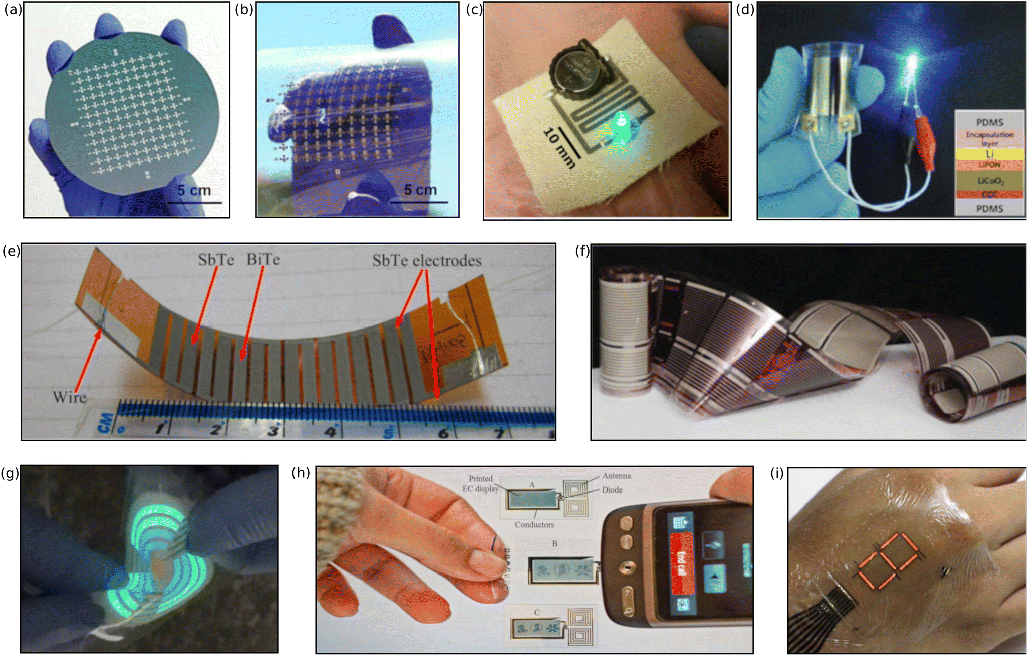 | ||
| Fig. 1 Printed electronics applications. (a) and (b) Fully screen-printed SWCNT TFT arrays on rigid and flexible substrates.13 Reprinted with permission from American Chemical Society, copyright 2014. (c) Inkjet-printed paths using silver nanoparticle inks on cotton woven fabrics connected to a LED and a battery.10 Reprinted with permission from American Chemical Society, copyright 2017. (d) A flexible lithium-ion battery turns on a blue LED under bending.19 Reprinted with permission from American Chemical Society, copyright 2012. (e) Screen printed planar thermoelectric generator on the Kapton substrate.15 Reprinted with permission from Elsevier, copyright 2016. (f) Rolls of gravure-printed inverted OPV modules.20 (g) Fully screen-printed, multicolour electroluminescent displays in the bent and twisted states.24 Reprinted with permission from American Chemical Society, copyright 2020. (h) Printed e-label with the antenna-diode-display circuit.14 Reprinted from the National Academy of Sciences, copyright 2016. (i) Transfer printed seven-segment PLED displays as an example of epidermal electronics.421 Reprinted from the American Association for the Advancement of Science under a Creative Commons Attribution NonCommercial License 4.0, copyright 2016. | ||
Almost all electronic components require conductive electrodes based on highly conductive materials. Here the range of available materials is the broadest.4,25,26 The mainly used conductive materials are metal nanoparticles (NPs) and nanowires (NWs) from Ag, Cu, Ni or Au, to name a few,5,27–34 carbon nanotubes (CNTs),3,35–40 graphene platelets (GNPs),41–46 conductive polymers,47–49 transparent conducting oxide nanoinks (TCOs),50–52 semiconductor nanomaterials,53–57 and more recently also reactive inks (nanomaterial-free) with metallic compounds and complexes as precursors, converted to bulk metal in the post-treatment process.58–61 Optoelectronic devices such as displays, organic light emitting diodes (OLEDs), and solar cells additionally require transparent electrodes for a trade-off between transparency and conductivity.62–64 Semiconductor inks in the form of nanomaterials dispersions or solutions of conjugated polymers are used to fabricate transistors and optoelectronic devices,65,66 and various active materials are needed for the production of sensors.67–70 New frontiers are opening on the fabrication of all the above-mentioned applications with eco-friendly materials for disposable electronic devices,71–74 and new fields of hybrid approaches are emerging, such as patchable75,76 or ingestible bioelectronics.77,78 The selection of materials is mainly determined by the required physical properties of the devices, such as conductivity, but an additional functionality is often required, such as optical transparency or mechanical stability to bending, twisting and stretching, which is especially important for flexible electronics. In most cases, the final functionality of the electronic product is related to both properties of the ink and the substrate, and the synergy of both. Besides the rigid substrates (glass and ceramics), the key players in printed electronics are elastic substrates in the form of polymer foils25,79,80 or paper81–83 and textiles.10,84,85
A large variety of printing, deposition and writing techniques have been incorporated to fabricate electronic devices in the last decades. While the term printed electronics often also covers coating techniques such as spin, spray, dip, slot die, blade and bar coating, we will focus here only on the printing techniques allowing for selective patterning of devices and circuits. This is especially important because selected 2D printing techniques are also used for the 3D printing of electronics. To briefly introduce to the reader some of the applications of the coating techniques, it is worth mentioning that they are often used for processing transparent electrodes or large-scale photovoltaics, and the coating processes can be easily scaled up and are adaptable to large-scale roll-to-roll production. In the group of the most popular printing techniques used in printed electronics applications, several are the key players, including screen printing (flatbed and rotary),20,86–89 gravure and rotogravure,20,90–92 flexographic,93,94 and offset printing.95,96 All techniques mentioned above are in the group of contact printing, which means that the tool (mask, matrix, stencil) is in direct contact with the substrate during the deposition process. These techniques also require the fabrication of patterned, indispensable masks, thus often introducing high setup costs and time. On the other hand, we have a series of non-contact techniques. This group is also highly exploited in the research and applications of printed electronics technology. Among the non-contact printing technologies, two techniques gained a lot of interest: ink-jet printing56,69,82,97,98 and Aerosol Jet Printing (AJP).12,99–101 The ink-jet technique can be additionally divided into Drop-On-Demand (DOD), continuous ink-jet printing and electrohydrodynamic jet printing, with the first being the most popular among the non-contact, maskless printing techniques. All these maskless techniques are often called digital printing, meaning they do not require additional mask fabrication, and the design can be directly printed on the Computer Numerically Controlled (CNC) setup. One of the serious drawbacks of the ink-jet technique is the use of low-viscosity inks to avoid nozzle clogging,102 limited for AJP.99
Due to the nature of several contact printing techniques and the incorporation of masks or stencils for the selective deposition of inks, their use is severely limited or even impossible in 3D additive manufacturing. At the same time, maskless non-contact printing techniques (ink-jet and AJP) have attracted significant attention in the area of additive manufacturing. Moreover, the translation from 2D to 3D printing with these digital techniques is very efficient. Therefore the two above-mentioned maskless, non-contact jet techniques will be covered in detail in further sections of this review.
3 Additive manufacturing – the enabler
Additive manufacturing is called by many names, but the most popular term is 3D printing. With the definition from the American Society for Testing and Materials (ASTM), it is ‘a process of joining materials to make objects from 3D model data, usually layer upon layer’.103 In other words, it is a computer-controlled fabrication of a three-dimensional object, with the material being sequentially deposited layer-by-layer along the Z-axis, from the computer-generated slicing code of the object.104 There are two basic 3D printing technologies based on the selective treatment of material: deposition from a nozzle (polymers, inks) and batch solidification (liquids, powders), with minor modifications (i.e. binder jetting of ink onto the powder). Detailed subdivision into several categories differing mainly by the method of layer deposition and fixation as well as by the used material is described in further sections (Fig. 2). A lot of similarities can be observed with the previously mentioned digital printing techniques while 3D printed structures are first digitally constructed as 3D models with computer-aided design (CAD) software, and later this geometry is interpreted and synthesized into a machine code which the 3D printer uses to produce bulk solid objects. Therefore no additional tools are fabricated, such as press stamps or injection moulds. Thanks to that, 3D printing profits from the capability to create geometrically complex constructs with low cost and minimal material waste. Initially developed as a rapid prototyping technique, 3D printing has become increasingly accessible with the advent of low-cost desktop 3D printers,105 gained more powerful traction with the development of novel printing technologies,106–110 and now stepping into professional applications such as the aerospace and automotive industries.111–116 While primarily developed for mechanical and construction element fabrication, 3D printing also spread beyond industry, especially in the field of medicine, addressing clinical needs, creating personalized implants and prostheses,117–121 regenerative scaffolds,122–124 drugs and drug delivery devices,78,125–127 or even enabling printing of living cells, leading to the creation of biological tissues and organs.128–131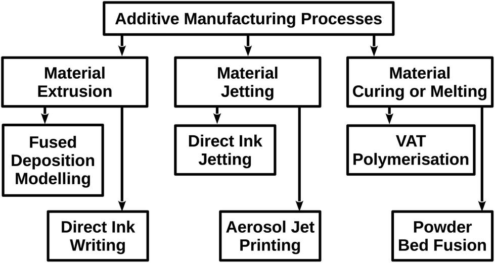 | ||
| Fig. 2 Selected additive manufacturing processes most suitable for 3D printed electronic applications. | ||
Having such tremendous technology in our hands, it was just a matter of time to implement additive manufacturing techniques for fabricating elements and circuits in electronics technology through combining the advances of printed electronics technology. As such, the enabling possibility of fabricating 3D structural electronics emerged. But only selected techniques are adaptable for printing electronics, and here, in this section, we will look closer at several of the most popular 3D printing techniques concerning their possible applications in 3D printed electronics fabrication. At the end of this section, other 3D printing additive techniques that have not yet gained much attention for producing electronic devices are also briefly mentioned.
The general concept of additively manufactured structural electronics is based on the fabrication of 3D structures with multilayered circuitry by selectively applying conductive and insulating materials to each layer, connecting them with interlayer conductive paths and additional mounting of non-printable discrete electronic components or small subsystems like integrated circuits (Fig. 3).132–134 Fabrication of paths and basic elements can be achieved via conformal printing without 3D printers, but selective printing techniques allow fabricating truly structural bulk circuitry embedded inside casings or construction elements. In the literature, we can find many successful attempts to fabricate various 3D printed electronic components and devices with different architectures to demonstrate the potential of additive manufacturing, yet readers need to be advised that the “3D printing” term is consequently overused most of the time for planar printing techniques. Most often, “additive manufacturing” is used for all additive approaches for fabricating electronic components. This is because printed electronics, involving multiple passes and building planar devices layer-by-layer, is, in fact, also an additive approach, and this is the source of misunderstanding. In this review, the focus is on printing techniques fabricating as much as possible spatial 3D objects (according to the mentioned ASTM definition), with embedded components, vertical interconnects, bulk load-bearings etc., or at least conformal ones on 3D substrates (thin-film ink-based techniques). Wherever possible, examples of impressive achievements of 2D printed electronics are presented, with great potential for implementation in the 3D printing of electronics (in analogy to ink-jet utilising the same concept as PolyJet).
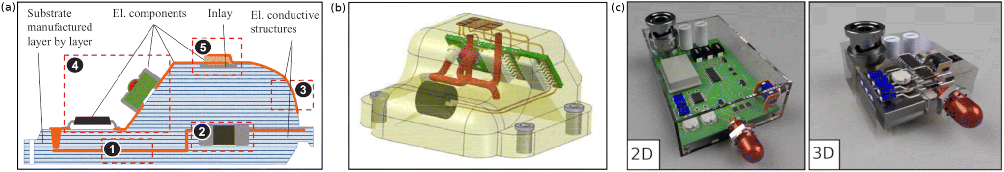 | ||
| Fig. 3 Opportunities for the adaptation of structural electronic circuits with embedded conductive tracks and components. Examples (a)132 and (b)133 reprinted from Elsevier B.V., under Attribution-NonCommercial-NoDerivs 3.0 Unported license, copyright 2014. (c)134 Reprinted from MDPI, Basel, Switzerland, under Creative Commons Attribution 4.0 license, copyright 2022. | ||
3.1 Fused deposition modeling – FDM
One of the most popular and widespread additive techniques is Fused Deposition Modelling (FDM, a brand name of Stratasys), also called Fused Filament Fabrication or Filament Freeform Fabrication (FFF). It is in a group of selective deposition of a liquid/melted material. The principle of this technique is based on extruding a thermally molten or semisolid material through a nozzle, followed by its solidification through cooling, to form a single layer, and the process repeats for the second layer.135–137 During the FDM process, the thermoplastic filament is fed from a spool and melted by the heated extruder head to decrease the viscosity. The melted filament is mechanically extruded through the tip of the nozzle by pressure induced from feeder rollers transporting the filament. The heated nozzle is positioned to perform planar movement according to the preset profile trajectory. The extruded filament is cooled shortly after deposition, progressively adhering to the build plate or previously cured layers. This process is defined by the resolution categories: Z resolution, XY resolution, and the minimum feature size.138 Resolution on the Z axis corresponds to the minimum layer height. In techniques such as FDM (or later described optical techniques), this value is correlated with the resolution of the motors driving the build plate or printer nozzle. The same applies to the XY resolution corresponding to the minimum horizontal movement of the build plate, nozzle or the optical imaging system. The XY resolution determines the minimum feature size, which can be defined as the smallest horizontal feature allowable to be printed. This is also related to the feature size determined in the FDM process by the diameter of the nozzle.108 In standard FDM equipment, the minimum feature size is in the range of 100 μm, and the printing speed defined by the length of the filament extruded via the nozzle is in the range of 1–10 m min−1.139–141Fig. 4a shows the working principle of the FDM technique.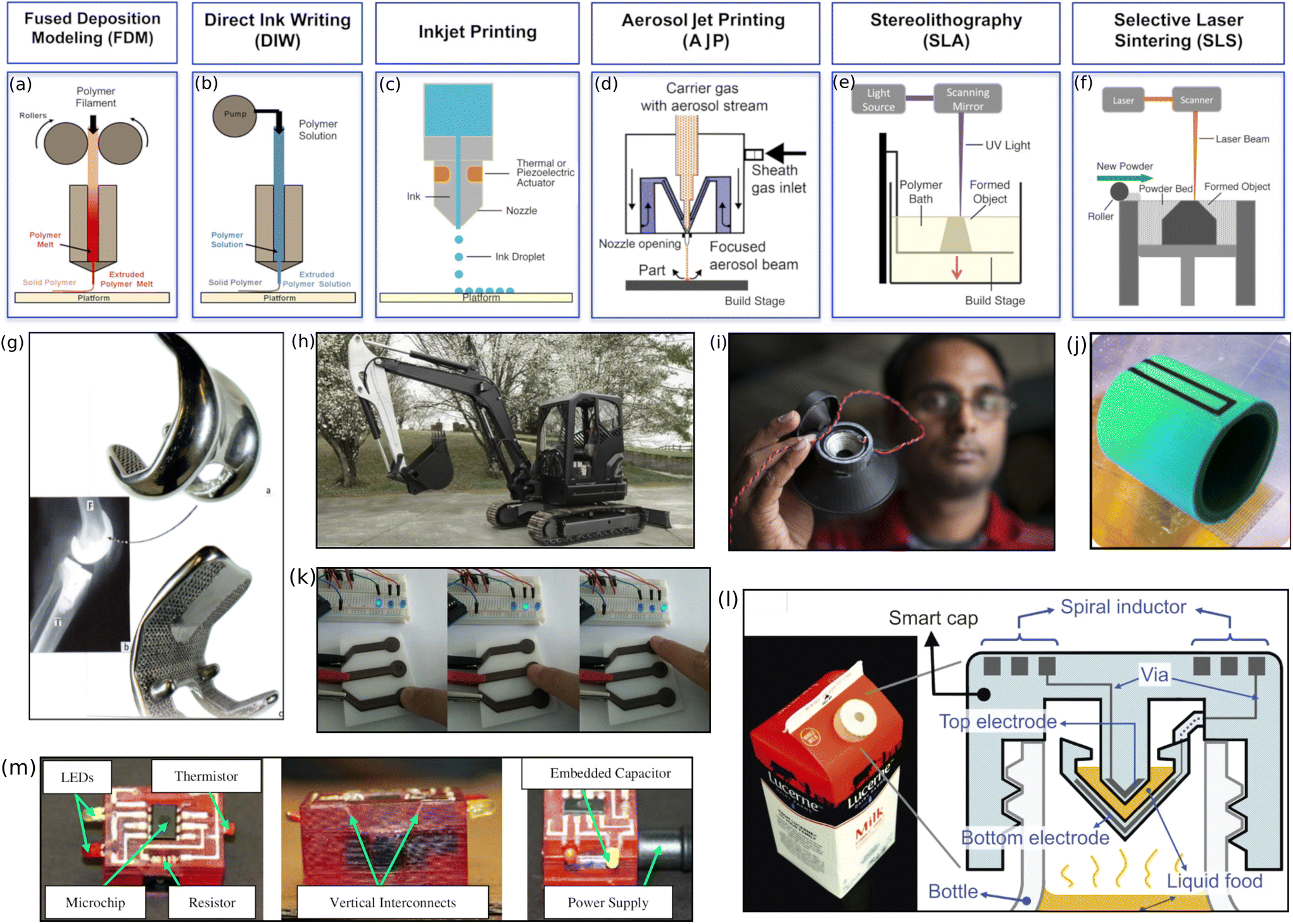 | ||
| Fig. 4 Schematic illustration of selected 3D printing techniques: (a) extrusion-based methods such as fused deposition modelling (FDM) and (b) direct ink writing (DIW), (c) inkjet printing and Multi-Jet techniques, (d) aerosol jet printing (AJP), (e) UV resin-based method stereolithography (SLA) and (f) powder-based methods such as selective laser sintering (SLS). Figures (a–c, e, f),120 copyright 2016, and (d),182 copyright 2013, reprinted and adapted with permission from American Chemical Society. (g) Knee inserts from a Co–Cr–Mo alloy fabricated with the EBM technique.121 Reprinted with permission from Elsevier, copyright 2017. (h) Full-size working excavator equipped with a 3D printed arm containing incorporated hydraulic lines fabricated with the WAAM/mBAAM technique.206 Reprinted with permission from Elsevier, copyright 2019. (i) Functional 3D printed loudspeaker with combined FDM and DIW techniques.223 Author Jason Koski, reprinted with permission from Cornell University Photography. (j) 3D printed capacitive ‘smart’ vessel.225 Reprinted from PLOS, under Creative Commons Attribution License, copyright 2012. (k) Human interface device (HID) FDM printed from a high-conductivity copper-filled composite.226 Reprinted from Springer Nature, under Creative Commons Attribution 4.0 International License, copyright 2018. (l) 3D printed “smart cap” for rapid detection of liquid food quality featuring wireless readout.228 Reprinted from Springer Nature, under Creative Commons Attribution 4.0 International License, copyright 2015. (m) Fabrication of the 3D 555 timer circuit with SLA and DIW techniques.230 Reprinted with permission from Emerald Publishing Limited, all rights reserved. | ||
The leading materials for the FDM technique are various thermoplastic polymers that can be thermally melted and extruded.141,142 Such a thermoplastic filament from polymers or composites has to be prepared beforehand using other extrusion processes in the form of filaments, with a standard diameter according to the printer's nozzle. Optionally FDM printers can be equipped with a hopper and a screw extruder, as in the injection moulding process, to directly extrude thermally melted polymer pellets via a heated nozzle.143,144 Polymers required for FDM processing are usually from the most popular group of acrylonitrile butadiene styrene copolymers (ABS), polylactic acid (PLA), polycarbonate (PC), polyurethanes (PU), polyphenylsulfone, poly(ether ether ketone), and poly(ether imide).141,145
The main advantages related to the use of the FDM technique, to name a few, are the relative simplicity and low cost of the equipment (printers can cost as little as a few hundred dollars), widely available polymer filaments and a relatively high print speed.105,141,146 The main disadvantages are related to the fabrication of supporting structures required for free-standing models (in contrast to a powder bed system), relatively low resolution in terms of precise electronic devices and possible nozzle clogging for viscous composite filaments. Nevertheless, the most significant advantage in the scope of electronics printing is easy integration to achieve multi-material printing,135,147 which could be easily implemented by simply adding as many printing nozzles as the number of materials needed to be processed.
3.2 Direct ink writing – DIW
Direct ink writing (DIW) is a very similar technique to the above-mentioned FDM printing, except that the printing material used here is in the form of a viscous functional ink instead of a filament, and there is no thermal melting of the material. The functional ink stored in the syringe container is extruded using pressure from a needle-like nozzle and deposited on a substrate or a previous layer.148 Pressure is generated on the piston via a pneumatic gas pump or motor-driven screw. The materials used here are in the form of low-viscosity inks flowing easily through the nozzle or shear-thinning pastes requiring a much larger driving force. When using low-viscosity inks, a curing system is used to cure the extruded filament instantly, allowing the retention of its 3D structure. Such post-processing steps used to solidify the extruded ink are related to photopolymerization or thermal curing.108,148 A modification of this process uses an additional shear thinning fluid, or a high viscosity gel, as a supporting matrix in a reservoir, with a nozzle injecting a low viscosity filler material into this supporting matrix.149 In standard DIW equipment, the minimum feature size is in the range of 1–500 μm, heavily ink dependent,148,150,151 and the printing speed defined by the volume of the extruded paste via the nozzle is in the range of 100–1000 mL h−1.148,152,153 Other process parameters related to the XY and Z axis resolution remain similar to the FDM technique due to many similarities in the equipment construction. Fig. 4b shows the working principle of the DIW technique.Direct ink writing is a highly flexible technique regarding the used material. Inks can be formulated from polymeric and colloidal suspensions or even adapted from printing techniques such as screen-printing.154 The range of viscosity for the materials is large, from liquid to paste, usually in the range of 102–108 [cP].155–157 Due to this, various suspensions, shear-thinning fluids, gels, foams, composite mixtures, and even biological cells can be printed.158–162
DIW offers many benefits, including printing at room temperature, the versatility of materials, including biological inks, and the easy fabrication of free-standing structures.163,164 Some disadvantages are related to complex ink formulation for small feature sizes, and using various binders can result in inferior electrical properties.108 Similarly to FDM, DIW offers a distinct advantage for 3D printed electronics as the implementation can be done easily with multiple nozzles and multi ink reservoirs, which allows integrating multiple functionalities in a 3D printing format.165,166
3.3 Direct ink jetting
A different approach for the selective deposition of a material is direct ink jetting, with several names used, such as ink-jet for the printing industry and printed electronics or Poly-Jet, Multi-Jet used in additive manufacturing for the description of 3D printing. As mentioned previously in the Printed electronics – the origin section, the most often used technique is Drop-On-Demand (DOD), with thermal or piezoelectric actuators propelling low-viscosity inks and ejecting droplets from micrometre-sized nozzles onto a build plate.167–169 Thermal printers heat the ink in microseconds, thermally expanding the ink volume (forming a bubble), and force a drop of ink through the nozzle, while piezoelectric printers apply voltage to a piezoelectric membrane attached to a glass tube, changing the pressure inside the ink chamber propelling a droplet through the nozzle. Deposited 2D patterns are instantly photo-cured under UV irradiation by the lamp attached next to the printhead.170,171 In low-viscosity ink techniques such as Multi-Jet, the droplet thickness determines the Z resolution. Ink droplets as small as 2–12 pL can be deposited with this method, resulting in a thin layer of a few micrometres even down to the sub-micron scale.171,172 Similarly to the FDM and DIW techniques, XY minimal resolution corresponds to the horizontal movement of the build plate or printhead, and it is in the range of 5–100 μm, additionally determined by a footprint of the deposited ink droplet.108,170,173 The printing speed defined by the volume of the deposited ink is in the range of 100–1000 mL h−1 for multi-head multi-nozzle systems.170Fig. 4c demonstrates the working principle of the Multi-Jet 3D printing technique.Ink-jet techniques require very low viscosity inks for efficient printing and the ink has to be precisely formulated to prevent nozzle clogging.102 Usually there is very limited range of viscosity values that can be used, most often <0.25 Pa s.170,174,175 Similarly to DIW and further discussed AJP, the deposition of ink without high temperatures allows for the deposition of a wide range of thermally fragile and living biological materials.130,176
The main advantages of ink-jet based techniques are related to the use of various substrates, limited waste production, easy application of a low-viscosity solution, and most of all high printing resolution, crucial for high-integration devices like transistors. The drawbacks are mostly related to the high risk of nozzle clogging with high-loaded inks, limiting the ink formulation, the observable “coffee-ring effect”,177,178 affecting the sub-micron quality of the printed features, and the need for complicated and expensive microelectromechanical multinozzle systems to print with a high speed. At the same time this technique is one of the most widespread applications in printed electronics and is rapidly expanding also in 3D printed electronics applications thanks to its easy adaptation to multimaterial deposition, with the use of multiple print heads.170,175
3.4 Aerosol jet printing – AJP
One of the well-known and fast-growing non-contact techniques in printed electronics and additive manufacturing, complementary to ink-jet, a direct write, is Aerosol Jet Printing (AJP). Compared with ink-jet techniques, AJP is a newly developed technology used for printing on both flat and non-flat substrates. It shares many similarities with the previously mentioned techniques, except the material deposition. In AJP, a low-viscosity ink is converted into an aerosol, compressed into a focused stream, and ejected from a nozzle with a high speed. In this technique, an atomizer (pneumatic or ultrasonic) converts the liquid functional ink into an aerosol of micrometre scale diameter droplets. Such prepared aerosol mist is transported to the print nozzle by a carrier gas flow and enwrapped by additional sheath gas flow in the print head cylindrically. Aerodynamic interaction between the sheath gas stream and the aerosol stream allows the efficient formulation of a sharp aerosol stream, exiting the nozzle tip to be deposited onto a substrate with a high speed.179Fig. 4d shows the working principles of the AJP process. The XY resolution is determined by the positioning system, as for FDM or DIW techniques. The minimum feature size (line density and width) related to the diameter of an aerodynamically focused stream is down to 10 μm, and the thickness (Z resolution) is comparable to ink-jet with a few hundred nanometers thick layers.179,180 The printing speed defined as the volume of the deposited material is up to 1200 mL h−1.181Aerosol jet printing is also an ink-based technique and thus requires low-viscosity inks, although it is more flexible than ink-jet printing due to the efficient use of two atomizing methods (pneumatic or ultrasonic) and allows for ink solutions and dispersions with the viscosity in the range from 1 to 1000 [cp],179,182 enabling the use of a wide range of inks with metals,101 carbon-nanomaterials,12 ceramics183 and biological materials.184
The general advantages of this technique are similar to other ink-based techniques, with the versatility of the materials used, the ability to easily deposit nanoparticles without the clogging problems observed for the ink-jet technique, and application of various substrates, with the most significant high-resolution of print. As a disadvantage, the most visible is the complexity of the system generating high-cost of implementation, also the use of particles is limited mostly to nanoparticles in the inks, and the printed line morphology (width, thickness, roughness) is influenced significantly by the atomization settings, the sheath gas flow rate, the carrier gas flow rate and the print speed that need to be controlled simultaneously.180,182 But the most powerful advantage of AJP in the scope of 3D printed electronics applications is the ability to print on non-planar complex surfaces because of the high stand-off distance (up to 5 mm) between the nozzle and the substrate, which makes it more tolerable to the non-uniformity of the substrate's surface.101 Also, this technique has the uncommon ability to print in multiple directions, including upwards and on complex surfaces, such as on five orthogonal sides of a cube.180 Readers are advised to get familiar with the impressive demonstrations of the capabilities of the AJP technique for printing on complex surfaces, inducing a golf ball.185
3.5 VAT polymerisation
3D printing methods using light to solidify selectively photocurable resins in tanks are generally called VAT polymerisation additive manufacturing. This term is rarely used to describe selected 3D printing techniques, while the most common in use are stereolithography (SLA) and Digital Light Projection (DLP) stereolithography. The other most influencing techniques in that group are Two-Photon Polymerization (2PP) and Continuous Liquid Interface Production (CLIP). In the further sections, I will refer to the whole group of photocurable resin-based techniques as VAT or SLA, and if needed, their distinct names will be used. SLA was one of the first developed 3D printing methods and is one of the most widely used additive techniques. It uses a tank of photocurable resin which is selectively photopolymerized by an ultraviolet (UV) laser to create one volume element (voxel) at a time.186,187 Once a layer of resin is solidified, the build platform retracts (Z step down), and a new layer of resin is introduced. Other resin-based techniques share many similarities, for example, Digital Light Projection (DLP) lithography188,189 and continuous liquid interface production (CLIP)190 also precisely solidify the photocurable resin, but are able to solidify an entire layer of resin at a time. On the level of one layer, they are almost identical to the well-known photolithography procedure used for the fabrication of electronic printed circuit boards (PCBs). Instead of SLA's point-wise light projection, the DLP technique accomplishes one layer using a dynamic mask in the form of a micromirror device191 or a liquid crystal display192 projecting a complete 2D pattern on the liquid resin. The CLIP technique accelerates the process by incorporating an oxygen-permeable window, enabling a 10 μm layer of uncured resin to exist between the window and the part, which allows images to be continuously projected, and the part can be steadily drawn out of the resin as one print instead of a set of layers.190 The 2PP technique also uses a laser, here an ultrashort IR (infrared) femtosecond laser pulse is focused on the point in the resin basin to polymerize a tiny voxel within the resin, enabling an exceptional 100 nm feature size but a very low volume of 1 cm3.106 For VAT 3D printing systems, Z resolution is similar to FDM or DIW techniques, related to the resolution of the motors driving the height of the build plate. Here, the XY minimum feature size is determined by the spot size of the laser for SLA (10–200 μm)187 and pixel size for DLP-based techniques (range of micrometres).191,192 The fabrication speed is among the fastest in 3D printing, reaching 106 mm3 h−1 for SLA, and even ten times faster for DLP and CLIP techniques.190,191Fig. 4e demonstrates the SLA printing technique.Materials selection for SLA is limited, as they all need to be photocurable resins. This is very similar to the previously mentioned Multi-Jet technique. Within this group, we can find a lot of different materials with various physical properties, especially with different mechanical properties. Yet, the fabrication of conductive or bioactive materials is difficult or sometimes impossible due to the use of crosslinkers and catalysts that are UV activated.193
The advantages of VAT polymerisation techniques relate to a very smooth surface in comparison with FDM, higher overall resolution, and high throughput, all these with relatively low-cost equipment.190,194 Unfortunately, for SLA and similar techniques, we face the synergy of the most impactful disadvantages of additive manufacturing: limitation to a single material printing and need for photocurable resins, both creating problems in the fabrication of electrically conductive components. Some of the rare multi-material VAT solutions will be listed in the Perspectives at the end of this review.
3.6 Powder bed techniques
Besides the most popular deposition and polymerisation techniques, it is also necessary to mention a vast group of powder-based techniques. Although their use in 3D printed electronics fabrication is very limited, they play a key role in the automotive and aerospace industries or mass production of implants for biomedical applications. Powder-based technologies utilize the material in a solid state (powder) from a vast range of functional materials (plastics, ceramics, and metals). These techniques share many similarities with the previously mentioned VAT polymerisation techniques, while here the resin is substituted with powder, and different techniques for selective solidification of powder are used. For all these techniques, the basic principle is that the pattern of each deposited layer of powder is converted into a continuous solid. This conversion can be achieved by Selective Laser Sintering (SLS), Selective Laser Melting (SLM), Direct Metal Laser Sintering (DMLS), Electron Beam Melting (EBM), and by ink-jetting a binder on the layer of powder (Binder-Jet) that might be additionally sintered with an IR lamp in Multi-Jet Fusion techniques (MJF)195–199 or post-processed in furnaces for sintering ink-jet binding metal powders like Metal-Jet.200,201 As an example of powder techniques, in SLS, instead of a photocurable resin, a bed of polymer, ceramic, or metal powder is sintered (or melted for SLM) with a laser,198,199 after that the bed retracts, a fresh layer of powder is rolled onto the top of the part, and the process repeats. The powder bed is usually able to support the construct, and hence, no additional supporting structures are needed as required for FDM, SLA or Multi-Jet techniques. In this technique, resolution limitations are related to the size of the particles to be sintered (or bound) and the spot of the energy beam or the ink drop, but can still achieve a feature size of approximately 50–100 μm.198,199 Generally, XY and Z resolution is also drive-related as for the FDM or SLA techniques (movement of the build plate, nozzles or optics). Fig. 4f shows the working principles of the SLS technique.One of the biggest advantages of this group of techniques is fairly large availability of materials. Occasionally some techniques need no support for printed structures (SLS, MJF, and Binder-Jet), no thermal stress for the Binder-Jet technique, and mechanical properties comparable to milling or moulding (SLM, DMLS, and EBM) (Fig. 4g). At the same time, some disadvantages are related to the high porosity of the final parts, and for high-temperature laser or electron beam processes, thermal stresses have to be considered as they can cause distortion to the printed part.195,199 As for the VAT polymerisation techniques, the drawback for electronics applications is in the “one powder at a time” process, although bulk conductive metal parts are also possible to fabricate. And the same as for SLA, some attempts for multi-material fabrication will be presented in the Perspectives section.
3.7 Other techniques
A brief glimpse of other emerging additive techniques covers concrete extrusion for house building,202,203 Wire-Arc Additive Manufacturing (WAAM) incorporating wire-arc welding and a 6-axis robotic manipulator,204,205 Big-Area Additive Manufacturing (BAAM) being a sort of very large-scale FDM,206–208 Direct Energy Deposition (DED) involving the melting of metal powder with a high-powered laser beam,209 or liquid and molten metal ink-jet, FDM and DIW techniques.210–214 An example of a full scale excavator arm fabricated with the WAAM/BAAM technique is presented in Fig. 4h.3.8 3D printed structural electronics
Various 3D printing technologies have already been explored with polymer composites, metal and carbon nanomaterials, powders or other materials owing to the increasing research interest in the 3D printing of electronics. There have been a number of books, reviews and foresight papers published in the last decade on the applications of 3D printing of electronics.2,4,215–221 From the most promising and revolutionary concepts introduced in the literature, there needs to be mentioned a fully 3D printed loudspeaker with FDM and DIW techniques,222,223 followed by one of the most complete 3D electronic printers introduced to the market, combining FDM and DIW with low-viscosity, reactivity, and low-temperature cured silver inks exhibiting resistivity close to bulk silver.224 FDM printed composites were used for the fabrication of piezoresistive and capacitive sensors for smart gloves, smart vessels and tactile pads,225,226 large-scale composite magnets,207 and polymer composites highly-loaded with dielectric ceramic powders.227 By the combination of SLA and DIW techniques, a portfolio of 3D printed resistors, inductors and capacitors with a wireless “smart cap” for a milk package was prepared,228 including a functional electrical circuit with a 555 timer, an electronic gaming die, and a set of sensors embedded in a helmet,229–231 and a university-based startup prepared a low orbit satellite.232 Also, SLS techniques are used for the fabrication of electrodes233 and antennas234,235 from metal powders. Selected applications of additive manufacturing for the fabrication of functional components in the mentioned domains are presented in Fig. 4.4 3D printed nanomaterials – the game-changer
In previous sections, we saw how additive manufacturing could overcome the limitations of conventional subtractive manufacturing methods (i.e. machining) or formative methods (i.e. forging and casting) to create complex geometries and multifunctional, multi-material structures. These new perspectives provided by additive manufacturing to integrate various materials into multifunctional constructs enable the creation of unique electronic devices. Nanomaterial patterning with additive manufacturing techniques can be the enabler for harnessing their nanoscale properties and effects and the fabrication of active structures with electrical, mechanical, optical, thermal, magnetic and biological properties. In this section, we will briefly review the properties of selected nanomaterials suitable for electronic applications and look closer at the current achievements in the synergistic integration of nanomaterials with additive manufacturing technologies to fabricate 3D printed structural electronics.4.1 Nanomaterials
Nanomaterials are materials with one spatial dimension between 1 and 100 nm. Such small dimensions promote a range of unique properties related to the size and morphology of nanomaterials not explored previously with bulk materials, even on the microscale.236–238 The easiest one to explain is the surface area, which is substantially high for nanomaterials compared to their bulk counterparts, and it is unrelated to the building atoms of nanomaterials. Furthermore, a material with dimensions on this scale and significant values of the surface-to-volume ratio exhibits modified physical and chemical properties. The weakly bound surface atoms at the surface of the nanoparticles foster melting-point depression due to their reduced cohesive energy (300–400 °C instead of 1064 °C for Au),239 increase their chemical reactivity, and compared to the bulk material structure, the mechanical and electrical properties of nanomaterials are improved by increases of crystal perfection or reductions of defects.240,241 Such size-dependent effects arising from the nanoscale are sometimes directly perceived in our macro world, like Au or Ag nanoparticle solutions that appear purple or red, instead of yellow-orange or soft-white shiny colours of the bulk materials, respectively. And such effects can be tuned via the size of the nanomaterial particle and not their chemical structure.190,237 The same applies to the luminescence emission from quantum dots (semiconducting nanoparticles) with different diameters (1–10 nm) affecting the emission wavelength that is exploited to create LEDs and display devices with exceptionally high-colour purity.242,243 A great number of research studies are also conducted towards exploiting nanomaterials’ antiviral, antibacterial, and antifungal properties and their capacity to deal with pathogen-related diseases.244,245For the fabrication of 3D printed electronic devices, we have to have specific electrical, dielectric, magnetic, semiconductive and other properties. The simplest approach to harness the potential of nanomaterials is the fabrication of low-temperature sintered conductive nanomaterial traces enabling the electrical conductivity almost at the same level as the bulk material.246 For this, the most utilised material is silver nanoparticles (AgNPs).247 However, due to their high cost, a lot of work is directed to replacing them (and other noble metals, such as gold or platinum) with less expensive counterparts, such as copper, aluminium or nickel. Some major challenges exist in this field, while their oxidation under ambient conditions is considerably high, an inert atmosphere would be required during the fabrication process.248–250 To eliminate this obstacle, attempts are made to use additional reducing agents or coat the nanoparticles with other metals (i.e. Cu@Ag).58,60,251 While a highly developed surface promotes fast oxidation of nanoparticles, at the same time the increased surface area of metal and carbon nanomaterials allows creating novel devices, such as supercapacitors.252 At the nanoscale level, a non-magnetic element can become magnetic.253 Such small sizes also promote the quantum confinement effect as the motion of their electrons are confined to a higher degree than their corresponding bulk counterpart, creating plasmon resonance, enabling the creation of highly sensitive biosensors and improved solar cell efficiency.254–256 Other confinement effects provide metal-like properties in non-conductive materials. For example, boron in bulk form is not considered a metal, while a borophene (2D sheet of boron atoms) is an excellent conductor,257 similarly titanium aluminium carbide (Ti3AlC2) ceramics in a 2D-layered structure exhibit metal-like electrical conductivity,258 what most of all applies to the celebrity of nanomaterials, graphene.259–261 The intriguing feature of nanomaterials is also the influence of the crystallographic chirality along the 2D sheet. This is the most known electronic feature of the graphene sheet, being the foundation of carbon nanotubes (CNTs). Depending on the chirality angle (direction of electron transport in the hexagonal graphene sheet), carbon nanotubes can be almost metal-like conductors or semiconductors259,262 without the change in their chemical structure, remaining purely carbon-based.
The above-mentioned features have made nanoscale materials valuable assets for a wide range of applications, promising exceptional boosting of the performances of various electronic devices. Here comes the printed electronics technology and subsequently 3D printed structural electronics. But both these approaches require the preparation of nanomaterials (usually in the form of nanopowders) for the efficient deposition and fabrication of complex systems. Here, composites arise as the most efficient use of nanomaterials for the fabrication of bulk structures with enhanced physical properties. However, the complexity of composites and ink preparation deserves separate review papers, and readers are advised to explore other sources on this topic.263–266 The challenge is to do it efficiently and with the most optimised results with respect to the expected properties.
4.2 3D printing with nanomaterials for structural electronics
In the literature, we find a great number of review papers dealing with printed and 3D electronics with nanomaterials.4,181,267–271 Most papers presenting successful attempts to fabricate various 3D printed electronic components and devices are focused on the conductive paths, passive components, circuitry, antennas, and electrodes. Less information is presented regarding more problematic active components and photonic and energy devices. A large part of experiments is devoted to sensors, with these being close to the passive components but having a wide range of applications. The range of materials available for 3D printed electronics is limited compared to printed electronics. Most conductive materials are based on metals or carbon nanomaterials, although the second group exhibits several orders of magnitude higher resistivity.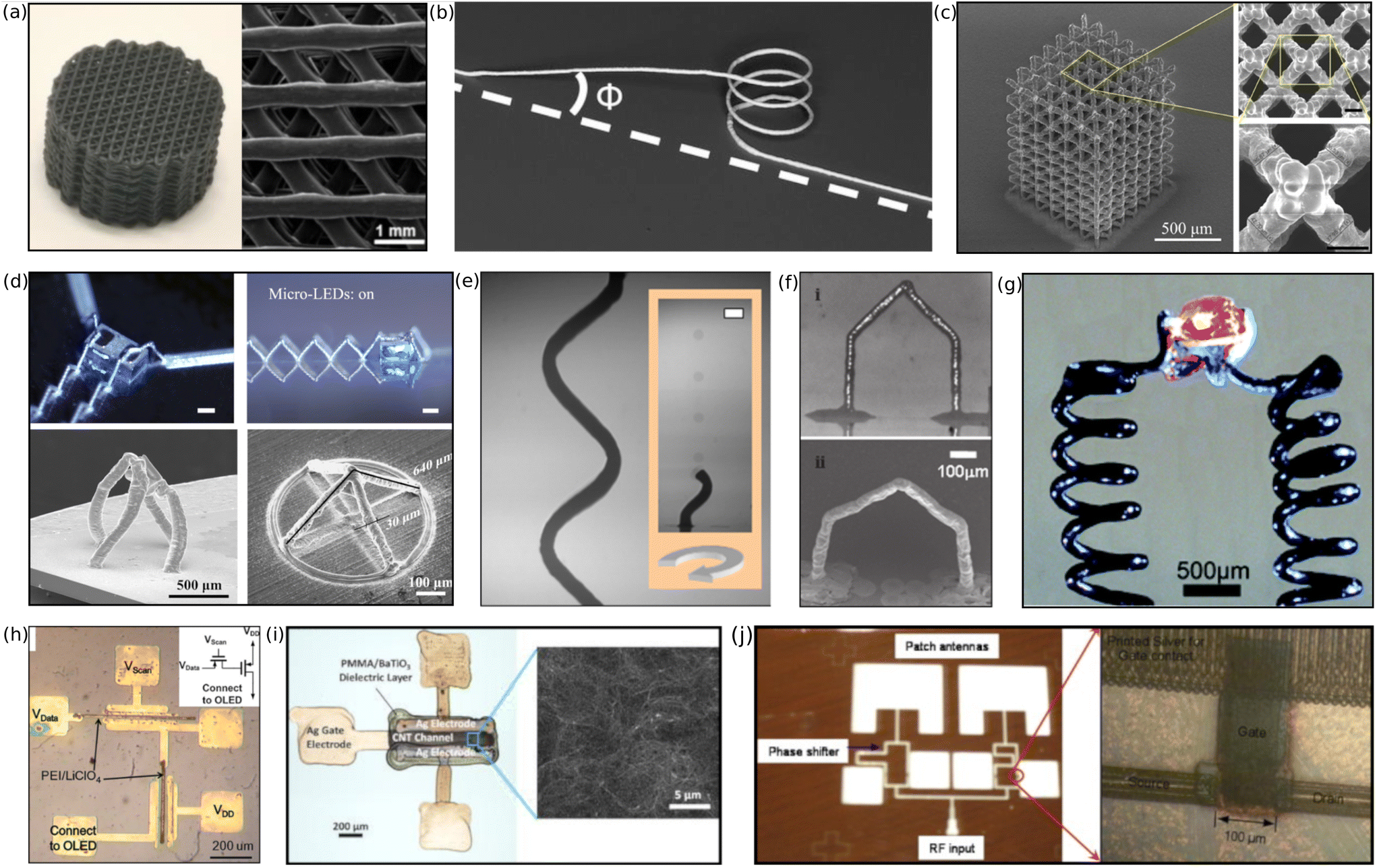 | ||
| Fig. 5 (a) FDM 3D printed porous part of LLDPE/GNPs, with the SEM image of the internal microstructure.274 Reprinted with permission from Elsevier, copyright 2021. (b) Freeform 3D metallic freestanding helical silver coils with diameter = 500 μm, fabricated with combined DIW and laser sintering.289 Reprinted with permission from the National Academy of Sciences, copyright 2016. (c) AJP printed microarchitectures with elements having a diameter of about 35 μm, and (d) stretchable spatial interconnects assembled between two micro-LEDs, also with spiral high aspect ratio hollow columns forming a dome.305 Reprinted from the American Association for the Advancement of Science, under Creative Commons Attribution-NonCommercial license, copyright 2017. (e) Micro helix and (f) micro bridge interconnector microstructures of metal NPs fabricated by modified ink-jet printing.303 Reprinted with permission from IOP Publishing, copyright 2010. (g) Optical image of two helical sensors DIW printed from electrically conductive PLA–MWCNT nanocomposite paste supporting and powering LEDs.313 (h) Control circuit made of two fully ink-jet printed top-gated SWCNT TFTs.316 Reprinted with permission from American Chemical Society, copyright 2011. (i) Fully AJP printed flexible photodetector using SWNTs, with the SEM image of the printed SWNT network on top of PMMA/BaTiO3.320 Reprinted with the permission of AIP Publishing, copyright 2017. (j) Photographs of the AJP printed SWCNT-based flexible device with printed TFTs.321 Reprinted with permission from Elsevier B.V., copyright 2010. | ||
While FDM composites are high-viscosity materials with dominant polymer dielectric bases, the idea is to incorporate conductive particles in less viscous and less dense matrix vehicles. Such an approach is possible with DIW pastes and ink extrusion techniques, where much higher loadings allow for achieving much higher conductivity values. With the application of conductive pastes and carbon nanomaterials also, conductive/resistive elements can be fabricated, although instead of thermal melting and extrusion of the composite filament, here the paste is extruded from the nozzle at room temperature and additionally cured by the evaporation of the solvent. This approach allows for the preparation of conductive compositions with GNPs or CNTs with loading as high as 40–60 wt% resulting in the conductivity values reaching up to 103 S m−1 for carbon nanomaterial-based lines.41,279–282 Other than heated solvent evaporation, also freeze drying is applied for 3D printing of silver NWs and graphene aerogels with combined DIW and ink-jet techniques.164,283,284 But the DIW technique has more advantages, especially in the use of metal nanopowders as inks and paste conductive fillers. Similarly to the use of carbon nanomaterials, a high loading of nanoparticles can be obtained here as well, yet additional thermal sintering of the deposited paste allows obtaining almost solid metallic lines. With the use of silver NPs with loading as high as 60–80 wt%, electrical conductivity in the range of 107 S m−1, close to the values of bulk silver or copper is possible.150,285–288 Although the DIW technique is often used for planar applications, with this technique it is possible to fabricate conductive 3D printed structures such as coils or grids (Fig. 5b).289 With the DIW technique also, a broader range of materials can be utilised, such as MXenes. With this group of materials and the DIW technique, various microelectronic, sensing and biological inks were prepared for the fabrication of electronic structures with conductivity up to 200 S m−1.290–292 Additionally, with the mixture of GNPs functionalized with Fe3O4 nanoparticles, DIW printed and thermally annealed, the obtained composites exhibited conductivity of 580 S m−1, and in addition, a saturation magnetization value of 15.8 emu g−1 was obtained.293
Of course, it is obligatory to mention ink-based techniques, such as AJP or ink-jet, further adaptable also Multi-Jet for 3D printing. As mentioned before, ink-based methods are often classified as 3D printing, while they actually fabricate thin layers. Only if the hybrid technique of Multi-Jet is applied the spatial elements are fabricated. Nevertheless, the applicability of the achievements of printed electronics with digital ink techniques such as ink-jet and AJP is enormous, and therefore the application of these selected ink-based techniques is intentionally presented in this review. The advantage of these techniques is the ability to incorporate metal nanopowders for further sintering processes, which is impossible for the FDM process. Also, a higher loading of carbon nanomaterials can be obtained (in the conductive layer) due to the lack of excessive polymer matrix, obligatory for the FDM process. Conductive lines prepared from metal nanoparticles, usually sintered at elevated temperatures, allow achieving with little effort resistivity close to the bulk metals.101,182,294,295 At the same time, carbon nanomaterials inks allow the fabrication of electrodes with conductivity a few orders of magnitude lower (up to 104 S m−1).177,296–300 Therefore more interesting approaches for the use of ink-based techniques will be listed regarding practical applications such as sensors or active components. But the ink-jet technique is also capable of fabricating multilayer, nonplanar circuits.185,301 A few publications mention the preparation of various conductive 3D microstructures (bridges, pillar arrays, helices, and zigzags) with the conductivity reaching 106 S m−1,302–304 and the same applies to the fabrication of 3D microlattices and other structures with the AJP technique (Fig. 5c and d).305
More exotic additive manufacturing techniques incorporated for the fabrication of 3D printed electronics are SLS and SLA. For the SLS (or SLM) technique, the approach is quite similar to the fabrication of construction elements, and regular metal powders can be used to form electrically conductive metal elements. Yet, for precise micro-components, silver and copper NPs are used instead of micro powders. With such adaptation, the electrical conductivity of 106 S m−1 is reached.289 With the SLS technique also, composite powders with carbon nanomaterials can be used. Sintered conductive 3D objects based on a 1 wt% CNT/TPU (flexible thermoplastic polyurethane) composite were obtained, exhibiting good flexibility and an electrical conductivity of 0.1 S m−1.306 For photoresin-based techniques such as SLA, there are no major breakthroughs in the fabrication of conductive elements. Few papers report results of the fabrication of 3D objects with in situ syntheses of conductive Ag NPs formed by UV irradiation of a photocurable resin and silver nitrate, with “measurable resistance” (500 kΩ)307 or graphene-based compositions subjected to thermal post-treatment reaching a conductivity of 10−5 S m−1.308
Having conductive electrodes, we are able to fabricate another passive element, a capacitor. Various research groups have demonstrated fully printed capacitors from silver and gold nanoparticle inks with the planar ink-jet technique,309,310 and with graphene/carbon-based conductive filaments with FDM,311 exhibiting a capacitance of 3.1 nF cm−2, 314 pF and 150 pF respectively. Also, multilayered capacitors and inductors fabricated with the ink-jet technique and AgNP inks, being very close to the Multi-Jet approach for 3D printing, were demonstrated.312 A large group of supercapacitors, having gained special interest regarding the application of nanomaterials, is described in further sections.
Being able to fabricate 3D metallic structures with DIW289 and ink-jet techniques302–304 opens the possibility of the fabrication of other passive components – inductors and antennas for various fields ranging from smart packaging, anticounterfeiting, healthcare to public safety applications (Fig. 5e and f). But carbon nanomaterials are also used for the fabrication of such components, and here DIW and FDM techniques play an important role. Based on the experiments of printing 3D free-standing conductive structures from CNT–PLA composites, such as 3D helix (inductor) (Fig. 5g),313 several attempts were made to fabricate 3D printed inductors for wireless charging application using the FDM printing technique,311 or 3D printed antennas for radio frequency identification (RFID) tags.314 A similar approach was also used for the fabrication of lightweight EMI shielding from 3D printed PLA/graphene nanocomposites, with reflection in the X-band frequency of 16 dB.315
On the other hand, we also need active components such as diodes and transistors, with these being the fundamental components of modern advanced electronic circuits. These components are typically multilayered and are built from different materials such as semiconductors, conductors, and dielectrics, i.e. channel, electrodes (drain, source, gate), and isolation dielectrics in the most simple transistor. On the mass scale, the fabrication of high-performance active components is based on silicon wafer technology. Yet, printed electronics for at least two decades has been working on the large-scale fabrication of printed diodes,14 transistors,310,316 and microchips (Fig. 5h).18,317,318 For the 3D printed electronics, the biggest restriction is in the structure of the transistor. The main principle is based on thin layer structures, and therefore none of the truly 3D printed techniques is capable of fabricating such fine features (in the range of μm), besides ink-jet (Fig. 5i)319,320 and AJP321 techniques (Fig. 5j). Therefore for the fabrication of high-efficiency active circuits, the need for the integration of 3D printing techniques such as FDM, SLA or SLS with ink-based techniques well developed for printed electronics still remains. As a closing note, it is worth mentioning that the direction for the development of high-performance silicon chips in the nm technology is based on the 3D structures of the channel and surrounding gate,322,323 but these structures are still fabricated with photolithography used in silicon technology, and not with additive manufacturing as described in this review.
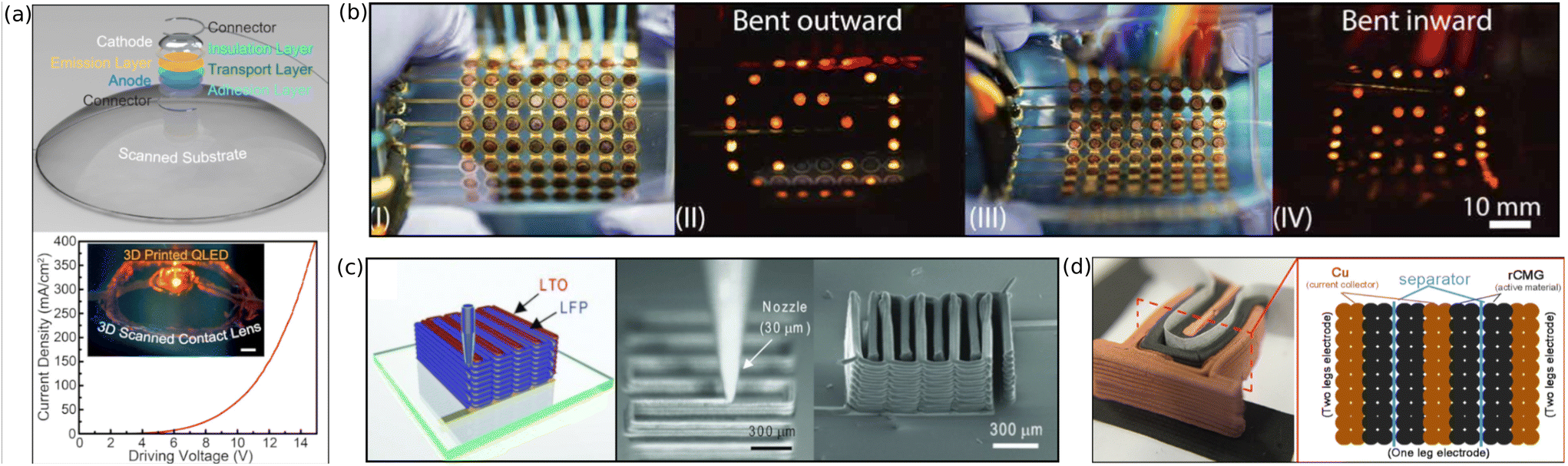 | ||
| Fig. 6 (a) 3D printed QD-LED onto a curvilinear contact lens.242 Reprinted with permission from American Chemical Society, copyright 2014. (b) 3D printed flexible OLED displays with the demonstration of different combinations of bending orientations.325 Reprinted from the American Association for the Advancement of Science under a Creative Commons Attribution NonCommercial License 4.0, copyright 2022. (c) 3D interdigitated microbattery architecture fabricated with the DIW printing technique.336 Reprinted with permission from John Wiley and Sons, copyright 2013. (d) FDM printed supercapacitor device including a cellulose paper separator and positive and negative electrodes, with a scheme of the cross section.338 Reprinted with permission from American Chemical Society, copyright 2017. | ||
Other techniques and applications cover, for instance, the preparation of graphene-based PLA composite filaments for the FDM technique to fabricate electrodes for pseudo-capacitors348 or submicron graphite PLA composites for printing electrodes to investigate the electrochemical performances of such 3D printed materials.349 Also the SLA technique was utilised to print capacitors from polymer composites containing silver NP decorated lead zirconate titanate powders (PZT), with the observable negative influence of Ag nanoparticles increasing the refractive index and thus decreasing the cure depth of the resin.350
DIW and FDM techniques play a major role in the fabrication of 3D printed sensors. Most often, carbon nanomaterials are used as functional fillers in inks and composites. One of the examples is a strain sensor from graphene–PDMS paste, printed in multiple directions to fabricate a sensor mesh,351 which is further modified with silica nanoparticles to enhance the mechanical and thermal properties.352 Several similar approaches utilising GNPs or CNTs can be found in the literature, as the preparation of carbon nanomaterial-based slurries for DIW printing is one of the simplest approaches for applying these nanomaterials for 3D printed sensors,353,354 (Fig. 7a and b) also with the use of food-inspired egg white as an organic hydrogel (Fig. 7c).355 One of the most impressive attempts to 3D print such structures with water-driven self-healable MWCNT–chitosan compositions for DIW is presented in the form of multilayered scaffolds, spider- and starfish-shaped objects (Fig. 7d).356 But besides carbon nanomaterials also, silver NWs and cellulose nanocrystals were adapted for ion detection in wireless sensor systems.357 The same applies to a mixture of cellulose nanofibers with MXenes for printing self-healable strain sensors, although printed with various shapes as one layer only, such a technique holds great potential for 3D printing.290 Of course, the variety of ink-based printing techniques applied for sensor fabrication is much wider, including AJP sensors from graphene for immunosensing358 or silver NP based for cerebral aneurysm monitoring359 but low viscosity ink techniques still have a long way for the fabrication of truly 3D printed elements.
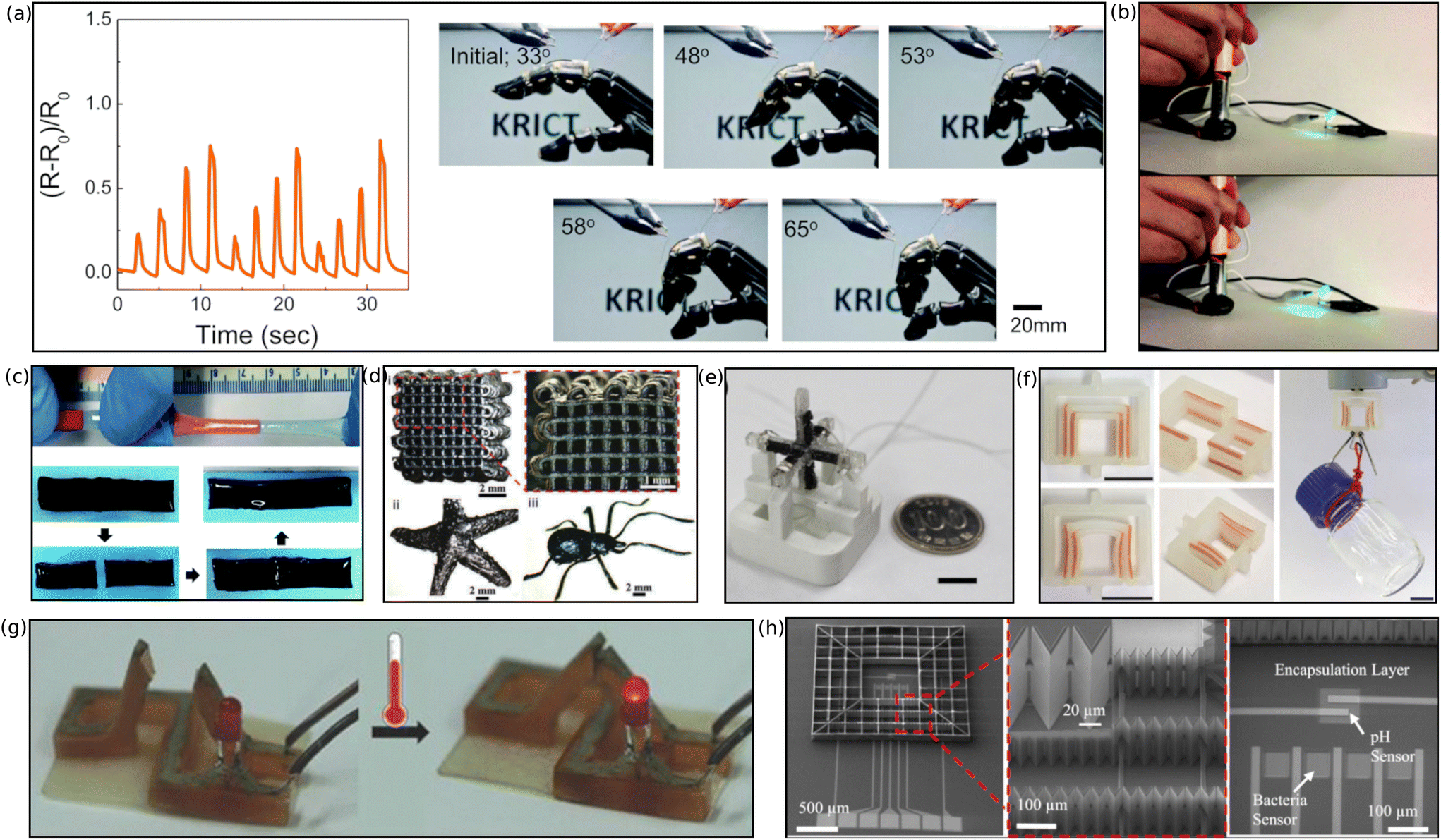 | ||
| Fig. 7 (a) DIW printed nanotube and graphene composite strain sensors for detecting robot finger motions with different bending angles.353 (b) 3D printed graphene-based hydrogel sensor demonstrating strain-dependent conductivity.354 (c) DIW 3D printed stretchable hydrogel from natural egg white for fabrication of electronic sensors and actuators, demonstrating a self-healing capability without any external stimulus.355 (d) Chitosan–CNT solvent composites for sensors, demonstrating 3D printed scaffolds as spider and starfish-shaped structures.356 (e) 3D cubic cross multiaxial force sensor on a FDM printed structure fabricated with CNT–TPU filaments.276 Reprinted with permission from Elsevier, copyright 2017. (f) Magnetically assisted 3D printed composite actuators.376 Reprinted from Springer Nature, under Creative Commons CC BY license, copyright 2015. (g) 3D printed shape memory-based electrical devices from carbon nanotubes with a temperature activated sensor in its “off” and “on” state.380 Reprinted with permission from John Wiley and Sons, copyright 2016. (h) A bio-inspired 3D printed graphene-based micro-structure for sensing of bacteria.388 Reprinted from Elsevier B.V., under Creative Commons CC-BY license, copyright 2019. | ||
Great potential also lies in the FDM technique and nanocomposites for the fabrication of sensors, as they do not have to exhibit exceptionally high conductivities and because the FDM technique is one of the most suitable techniques for the fabrication of bulk structures with embedded sensors. One of the most often described materials in the literature for FDM printing of sensors are CNT, GNP or other carbon-based composites with PLA and ABS. Commercial materials “carbomorph” and “blackmagic” are among the most often used materials for FDM fabrication of electronics.225,348,360,361 The electrical, thermal and mechanical properties of 3D printed MWCNT/ABS were also examined with respect to the influence of printing parameters, here the deposition direction, on the mechanical and electrical properties of composite sensors.362 Biomedical sensing systems play an important role in the studies on FDM printed composites with PLA and carbon nanomaterials due to the biocompatibility of such materials.362 A simple cone-geometry electrode printed from a carbon–PLA composite has been used in an ex vivo experiment over the gut tissue of guinea pig for monitoring the serotonin level and muscle contraction.363 Other approaches include PLA/graphene electrodes for the detection of H2O2,364 a mycotoxin (ZEA) compound,365 metal ions in biological specimens,366 glucose biosensing,367 and immunobiosensors for the detection of viruses.368 Using a similar material, a graphene–ABS composite, a 3D printed electrocardiogram (ECG) sensor was FDM printed and additionally coated with titanium and a gold layer to prevent corrosion and oxidation.369 Substituting the rigid ABS or PLA matrix with a flexible thermoplastic polyurethane matrix filled with MWCNTs allows for the fabrication of elastic strain sensors using the piezoresistive changes in materials properties.370 Also, MXene and CNT reinforced TPU composites were implemented for elastic strain sensors and electromagnetic shielding applications (Fig. 7e).276,371 Other nanomaterials can also be incorporated into the FDM polymer composites, such as ABS filled with magnetite nanoparticles (Fe3O4 NP) for the fabrication of glucose sensors,372 or immobilised on the surface of printed PLA/graphene electrochemical sensors, as presented for electrodes modified with gold nanoparticles (Au NPs) in the literature.373
Only a few examples present the utilisation of the SLA technique for fabricating composite sensors due to the obstacle in the preparation of conductive structures with VAT polymerisation materials. In one of the publications, work towards the integration of mechanical and electrical properties in complex 3D shapes is presented, which used graphene nanoplatelets aligned with an electric field during SLA printing for a 3D printed lightweight smart armour that can sense its damage with a hesitated resistance change.374 Also, a strain sensor array was fabricated from a UV curable resin with MWCNTs, with additional responses to humidity and temperature.375
Being able to print micromechanical fine structures and integrate them with electronic circuits end elements sparked the idea for the fabrication of lab-on-chip microsystems. Lab on a chip is defined as research towards miniaturizing biological or chemical processes, with input from microfluidics and miniaturized sensors (biochips), typically utilising time-consuming, multi-step lithographic processes to fabricate such MEMS systems.382 Here 3D printing emerged allowing for rapid customization and new applications with 3D structural electronics. An entirely DIW-printed lab on a chip consisted of carbon–TPU printed strain gauges, followed by electrical leads and contact pads printed with silver-nanoparticle polyamide ink and various insulating and support layers. This biochip micro-architecture allowed growth and monitoring of cardiac tissues over the course of a month.383 Also, a nanoparticle luminescent indicator ink was used with the DIW technique to print sensors integrated into scaffolds for the growth and metabolic activity monitoring of microalgae and mesenchymal stem cells.384 The micro-fluidics and micro-drive applications of the FDM technique include configurable 3D printed microfluidic lab on a chip reactionware devices for chemical syntheses, fabricated in just a few hours, used for gold nanoparticle synthesis.385 Furthermore, module-based microfluidic components were fabricated from polymers with FDM and integrated nano-/micro-particles as biosensors to detect the AFP antigen.386 An SLA printed microfluidic device with magnetic nanoparticles was used to actively remove and sort E. coli bacteria from a solution.387 A similar VAT technique, two-photon polymerization (2PP), was used to create a bio-inspired microscopic cage for motile bacteria to improve the sensitivity of a graphene-based biosensor (Fig. 7h).388
5 Perspectives
It is worth noting that during the preparation of this review, many new techniques and applications emerged or are under development and hence, they are not mentioned here. Secondly, only the most popular 3D printing techniques were taken into account, and tens or hundreds of other techniques and modifications exist that can also be applied for the fabrication of 3D printed electronics, just to name a few exotic ones such as fluid shear patterning, evaporative patterning, acoustic patterning, electrical patterning, magnetic patterning, optical patterning, thermal patterning etc.181 One of the most obvious areas of advancement lies in the implementation of ink-based techniques such as ink-jet and AJP for the fabrication of truly 3D structures, as presented previously for the rare application of AJP for fabrication of microlattices.305,342 The development of new materials is also progressing by visibly approaching MXenes for the fabrication of conductive and radio-frequency devices.389,390 Also, new forms of materials allow resolving some previously mentioned problems with the application of various nanomaterials, for instance, silver-coated copper nanopowder core–shell particles (CuNP@Ag),391 or Ni coated392 or Sn coated particles,30 for limitation or elimination of the reactivity of Cu NPs. This section covers also the area of interdisciplinary approaches combining commonly separated fields of research i.e. electronics and biomedicine.The broad area for development covers the preparation of a whole new branch of materials for VAT and Multi-Jet techniques, using both UV curable resins. Due to the mentioned restrictions related to the fabrication of highly conductive UV-cured composites, only dielectric, photonic, magnetic or highly resistive materials can be obtained, severely limiting the application of these techniques. Already many problems with the adaptation of VAT techniques for 3D printed electronics are observed, such as the negative impact on the polymerisation process with a high concentration of metal or ceramic and oxide nanoparticles,332,333,393 forcing additional sintering procedures to obtain conductive structures with silver NPs for ink-based techniques.394,395
Unfortunately, for VAT polymerisation and powder-bed techniques, there is a more fundamental restriction: one material at a time. While most of the extrusion or ink-based techniques, such as FDM or Multi-Jet, are easily adaptable for multi-material printing, it is extremely difficult for SLA and SLS techniques. This limitation is often solved by separate printing and attaching layers with different properties and materials,396,397 or by the replacement of resins or powders, leading to the repetition of the process.398–402 Such an approach significantly slows down the process, increases the overall manufacturing time, and poses the risk of cross-contamination between materials, which becomes even more apparent taking into account that frequent material change is needed for hundreds of layers with the increasing complexity of the part. Only the recent example of the VAT polymerisation technique deals with this problem, utilising a dynamic fluid control and exchange process, enabling a fast switch between liquid photopolymers, even including micro-/nano-particle suspensions. Such a technique was even used for the fabrication of actuators based on UV resins filled with Cu and Al2O3 nanopowder.403
In the scope of multi-material printing, the most frequent approach is introducing hybrid techniques, being a partial solution for the limitations of UV-cured VAT techniques and powder-bed ones. Already one of the most popular adaptations of the SLA technique for the fabrication of electronics is 3D printing of substrates, even 3D shaped, and filling specially prepared grooves with conductive inks, most often with DIW, ink-jet or AJP techniques.229–231,404 The same applies for the FDM or SLS printed substrates even for the fabrication of active components such as transistors.405 Additional laser sintering of metal NPs can be applied.288,406 While the binder-jet technique already uses ink-jet printing, the materials in one section of printing heads can be replaced with conductive inks or the AJP technique can be incorporated into the process.132
As we saw previously in the section regarding 3D printing of biomedical sensors or lab-on-chips and in the large section of 3D printed electronics, the most obvious next step is the combination of both of them. One aspect is the enhancement of functionality in both electronic systems and biomedical applications. The second one is related to the biocompatibility of carbon-based nanomaterials, which can additionally foster the development of 3D printed bioelectronics. Nanomaterials as additives are already used in 3D printed biocompatible substrates such as hydrogels to enhance bioactivity and cell viability. The seamlessly interweaved electronics with geometrically complex, biocompatible scaffolds and devices can additionally enhance already complex biological systems.407–411 A more advanced approach covers the use of FDM or DIW techniques and carbon nanomaterials in the fabrication of electrically conductive scaffolds for effective stimulation of cell proliferation for implants and biological tissues or organs.41,383 One of the most impressive achievements covers the use of DIW printing of a regenerative scaffold with living chondrocytes in the shape of an ear and co-printed with silver nanoparticles as a coiled antenna inside the ear, which is the most visible example of the possibility of integrating biological constructs with functional electronics.412 This topic is not entirely new, and readers can refer to several review papers covering 3D printed biodevices.413,414
4D is another approach. It has already been briefly mentioned with 3D printed actuators. With additive manufacturing, 3D printed origami electronics, self-assembling conductive structures, and bioinspired shape-changing systems are also fabricated.399,415–418 Finally, embedding interconnects is the topic for future works on 3D printed electronics for the integration of SMD-components419 followed by the effective design of 3D circuitry, including also toolpath planning and alignment of the 3D parts for optimal printing.420
The areas for exploration of 3D printed structural electronics with nanomaterials are vast and could also dig deeper into surface activation and growth of nanoparticles on 3D printed structures, selective electrochemical metallization of low conductivity carbon composites and SLA structures, especially important for high-frequency radio circuits or electromagnetic interference shielding. All breakthroughs and successes in the 3D printing of electronics mentioned in this paper allow reimagining our approach for fabricating electronics. However, many challenges remain for the application of nanomaterials for the 3D printing of electronics, and more efforts need to be made for this technology to be widely adopted in mass production by the electronic manufacturing industry.
Author contributions
M. S. investigated the literature, wrote the original draft, assembled the figures and revised the manuscript.Conflicts of interest
There are no conflicts to declare.Acknowledgements
This work was supported by the Foundation for Polish Science, within the project “Functional heterophase materials for structural electronics” (First TEAM/2016-1/7), co-financed by the European Union under the European Regional Development Fund; supported by the Institute of Metrology and Biomedical Engineering, Faculty of Mechatronics at the Warsaw University of Technology under the Excellence Initiative – Research University program (agreement no. 1820/108/Z11/2022). I want to express my deepest gratitude to Kacper Skarżyński for provoking me to prepare this review.Notes and references
- N. Shahrubudin, T. Lee and R. Ramlan, Procedia Manuf., 2019, 35, 1286–1296 CrossRef.
- H. H. Hamzah, S. A. Shafiee, A. Abdalla and B. A. Patel, Electrochem. Commun., 2018, 96, 27–31 CrossRef CAS.
- K. D. Harris, A. L. Elias and H.-J. Chung, J. Mater. Sci., 2016, 51, 2771–2805 CrossRef CAS.
- A. Kamyshny and S. Magdassi, Chem. Soc. Rev., 2019, 48, 1712–1740 RSC.
- D. McCoul, W. Hu, M. Gao, V. Mehta and Q. Pei, Adv. Electron. Mater., 2016, 2, 1500407 CrossRef.
- V. Subramanian and T. Lee, Nanotechnology, 2012, 23, 340201 CrossRef PubMed.
- H. Zhang, S. K. Moon and T. H. Ngo, Int. J. Precis. Eng. Manuf. – Green Technol., 2020, 7, 511–524 CrossRef.
- S. Niu, N. Matsuhisa, L. Beker, J. Li, S. Wang, J. Wang, Y. Jiang, X. Yan, Y. Yun, W. Burnett, A. S. Y. Poon, J. B.-H. Tok, X. Chen and Z. Bao, Nat. Electron., 2019, 2, 361–368 CrossRef.
- A. Rivadeneyra, J. Fernández-Salmerón, M. Agudo, J. A. López-Villanueva, L. F. Capitan-Vallvey and A. J. Palma, Sens. Actuators, B, 2014, 195, 123–131 CrossRef CAS.
- O. Nechyporchuk, J. Yu, V. A. Nierstrasz and R. Bordes, ACS Sustainable Chem. Eng., 2017, 5, 4793–4801 CrossRef CAS.
- K. Fukuda and T. Someya, Adv. Mater., 2017, 29, 1602736 CrossRef PubMed.
- M. Rother, M. Brohmann, S. Yang, S. B. Grimm, S. P. Schießl, A. Graf and J. Zaumseil, Adv. Electron. Mater., 2017, 3, 1700080 CrossRef.
- X. Cao, H. Chen, X. Gu, B. Liu, W. Wang, Y. Cao, F. Wu and C. Zhou, ACS Nano, 2014, 8, 12769–12776 CrossRef CAS PubMed.
- N. Sani, M. Robertsson, P. Cooper, X. Wang, M. Svensson, P. Andersson Ersman, P. Norberg, M. Nilsson, D. Nilsson, X. Liu, H. Hesselbom, L. Akesso, M. Fahlman, X. Crispin, I. Engquist, M. Berggren and G. Gustafsson, Proc. Natl. Acad. Sci. U. S. A., 2014, 111, 11943–11948 CrossRef CAS PubMed.
- Z. Cao, E. Koukharenko, M. Tudor, R. Torah and S. Beeby, Sens. Actuators, A, 2016, 238, 196–206 CrossRef CAS.
- A. M. Gaikwad, D. A. Steingart, T. Nga-Ng, D. E. Schwartz and G. L. Whiting, Appl. Phys. Lett., 2013, 102, 233302 CrossRef.
- P. Giannakou, M. G. Masteghin, R. C. T. Slade, S. J. Hinder and M. Shkunov, J. Mater. Chem. A, 2019, 7, 21496–21506 RSC.
- R. A. Street, T. N. Ng, D. E. Schwartz, G. L. Whiting, J. P. Lu, R. D. Bringans and J. Veres, Proc. IEEE, 2015, 103, 607–618 CAS.
- M. Koo, K.-I. Park, S. H. Lee, M. Suh, D. Y. Jeon, J. W. Choi, K. Kang and K. J. Lee, Nano Lett., 2012, 12, 4810–4816 CrossRef CAS PubMed.
- M. Välimäki, P. Apilo, R. Po, E. Jansson, A. Bernardi, M. Ylikunnari, M. Vilkman, G. Corso, J. Puustinen and J. Tuominen, et al. , Nanoscale, 2015, 7, 9570–9580 RSC.
- M.-S. Lee, K. Lee, S.-Y. Kim, H. Lee, J. Park, K.-H. Choi, H.-K. Kim, D.-G. Kim, D.-Y. Lee, S. Nam and J.-U. Park, Nano Lett., 2013, 13, 2814–2821 CrossRef CAS PubMed.
- G. Grau and V. Subramanian, Adv. Electron. Mater., 2016, 2, 1500328 CrossRef.
- S. I. Park, D. S. Brenner, G. Shin, C. D. Morgan, B. A. Copits, H. U. Chung, M. Y. Pullen, K. N. Noh, S. Davidson, S. J. Oh, J. Yoon, K.-I. Jang, V. K. Samineni, M. Norman, J. G. Grajales-Reyes, S. K. Vogt, S. S. Sundaram, K. M. Wilson, J. S. Ha, R. Xu, T. Pan, T.-i. Kim, Y. Huang, M. C. Montana, J. P. Golden, M. R. Bruchas, R. W. Gereau and J. A. Rogers, Nat. Biotechnol., 2015, 33, 1280–1286 CrossRef CAS PubMed.
- C. Zhao, Y. Zhou, S. Gu, S. Cao, J. Wang, M. Zhang, Y. Wu and D. Kong, ACS Appl. Mater. Interfaces, 2020, 12, 47902–47910 CrossRef CAS PubMed.
- R. Abbel, P. Teunissen, E. Rubingh, T. van Lammeren, R. Cauchois, M. Everaars, J. Valeton, S. van de Geijn and P. Groen, Transl. Mater. Res., 2014, 1, 015002 CrossRef CAS.
- M. Layani, A. Kamyshny and S. Magdassi, Nanoscale, 2014, 6, 5581–5591 RSC.
- A. Kamyshny and S. Magdassi, Small, 2014, 10, 3515–3535 CrossRef CAS PubMed.
- S. Kim, S. Won, G.-D. Sim, I. Park and S.-B. Lee, Nanotechnology, 2013, 24, 085701 CrossRef PubMed.
- D. Langley, G. Giusti, C. Mayousse, C. Celle, D. Bellet and J.-P. Simonato, Nanotechnology, 2013, 24, 452001 CrossRef PubMed.
- H. J. Park, Y. Jo, M. K. Cho, J. Young-Woo, D. Kim, S. Y. Lee, Y. Choi and S. Jeong, Nanoscale, 2018, 10, 5047–5053 RSC.
- B. Reiser, L. González-García, I. Kanelidis, J. H. M. Maurer and T. Kraus, Chem. Sci., 2016, 7, 4190–4196 RSC.
- Y.-H. Son, J.-Y. Jang, M. K. Kang, S. Ahn and C. S. Lee, Thin Solid Films, 2018, 656, 61–67 CrossRef CAS.
- W. Wu, Nanoscale, 2017, 9, 7342–7372 RSC.
- N. Sharma, N. M. Nair, G. Nagasarvari, D. Ray and P. Swaminathan, Flexible Printed Electron., 2022, 7, 014009 CrossRef.
- L. Cai and C. Wang, Nanoscale Res. Lett., 2015, 10, 320 CrossRef PubMed.
- Y. Che, H. Chen, H. Gui, J. Liu, B. Liu and C. Zhou, Semicond. Sci. Technol., 2014, 29, 073001 CrossRef CAS.
- K. Kordás, T. Mustonen, G. Tóth, H. Jantunen, M. Lajunen, C. Soldano, S. Talapatra, S. Kar, R. Vajtai and P. Ajayan, Small, 2006, 2, 1021–1025 CrossRef PubMed.
- P. N. Nirmalraj, P. E. Lyons, S. De, J. N. Coleman and J. J. Boland, Nano Lett., 2009, 9, 3890–3895 CrossRef CAS PubMed.
- S. Park, M. Vosguerichian and Z. Bao, Nanoscale, 2013, 5, 1727 RSC.
- J. Zaumseil, Semicond. Sci. Technol., 2015, 30, 074001 CrossRef.
- A. E. Jakus, E. B. Secor, A. L. Rutz, S. W. Jordan, M. C. Hersam and R. N. Shah, ACS Nano, 2015, 9, 4636–4648 CrossRef CAS PubMed.
- W. Li, F. Li, H. Li, M. Su, M. Gao, Y. Li, D. Su, X. Zhang and Y. Song, ACS Appl. Mater. Interfaces, 2016, 8, 12369–12376 CrossRef CAS PubMed.
- K. S. Novoselov, V. I. Fal'ko, L. Colombo, P. R. Gellert, M. G. Schwab and K. Kim, Nature, 2012, 490, 192–200 CrossRef CAS PubMed.
- M. H. Overgaard, M. Kühnel, R. Hvidsten, S. V. Petersen, T. Vosch, K. Nørgaard and B. W. Laursen, Adv. Mater. Technol., 2017, 2, 1700011 CrossRef.
- E. B. Secor, S. Lim, H. Zhang, C. D. Frisbie, L. F. Francis and M. C. Hersam, Adv. Mater., 2014, 26, 4533–4538 CrossRef CAS PubMed.
- D.-M. Sun, C. Liu, W.-C. Ren and H.-M. Cheng, Small, 2013, 9, 1188–1205 CrossRef CAS PubMed.
- W. Clemens, W. Fix, J. Ficker, A. Knobloch and A. Ullmann, J. Mater. Res., 2004, 19, 1963–1973 CrossRef CAS.
- B. Weng, R. L. Shepherd, K. Crowley, A. J. Killard and G. G. Wallace, Analyst, 2010, 135, 2779 RSC.
- C.-Y. Yang, M.-A. Stoeckel, T.-P. Ruoko, H.-Y. Wu, X. Liu, N. B. Kolhe, Z. Wu, Y. Puttisong, C. Musumeci, M. Massetti, H. Sun, K. Xu, D. Tu, W. M. Chen, H. Y. Woo, M. Fahlman, S. A. Jenekhe, M. Berggren and S. Fabiano, Nat. Commun., 2021, 12, 2354 CrossRef CAS PubMed.
- E. N. Dattoli and W. Lu, MRS Bull., 2011, 36, 782–788 CrossRef CAS.
- Y. Kashiwagi, A. Koizumi, Y. Takemura, S. Furuta, M. Yamamoto, M. Saitoh, M. Takahashi, T. Ohno, Y. Fujiwara, K. Murahashi, K. Ohtsuka and M. Nakamoto, Appl. Phys. Lett., 2014, 105, 223509 CrossRef.
- J. Song, S. A. Kulinich, J. Li, Y. Liu and H. Zeng, Angew. Chem., 2015, 127, 472–476 CrossRef.
- A. Kim, Y. Won, K. Woo, C.-H. Kim and J. Moon, ACS Nano, 2013, 7, 1081–1091 CrossRef CAS PubMed.
- M. M. Rehman, G. U. Siddiqui, J. Z. Gul, S.-W. Kim, J. H. Lim and K. H. Choi, Sci. Rep., 2016, 6, 36195 CrossRef CAS PubMed.
- J. J. Schneider, R. C. Hoffmann, J. Engstler, S. Dilfer, A. Klyszcz, E. Erdem, P. Jakes and R. A. Eichel, J. Mater. Chem., 2009, 19, 1449 RSC.
- X. Lin, J. Kavalakkatt, M. C. Lux-Steiner and A. Ennaoui, Adv. Sci., 2015, 2, 1500028 CrossRef PubMed.
- S. Lim, B. Cho, J. Bae, A. R. Kim, K. H. Lee, S. H. Kim, M. G. Hahm and J. Nam, Nanotechnology, 2016, 27, 435501 CrossRef PubMed.
- Y. Farraj, M. Grouchko and S. Magdassi, Chem. Commun., 2015, 51, 1587–1590 RSC.
- N. Komoda, M. Nogi, K. Suganuma and K. Otsuka, ACS Appl. Mater. Interfaces, 2012, 4, 5732–5736 CrossRef CAS PubMed.
- Y. S. Rosen, A. Yakushenko, A. Offenhäusser and S. Magdassi, ACS Omega, 2017, 2, 573–581 CrossRef CAS PubMed.
- D.-Y. Shin, M. Jung and S. Chun, J. Mater. Chem., 2012, 22, 11755 RSC.
- Y.-M. Chien, F. Lefevre, I. Shih and R. Izquierdo, Nanotechnology, 2010, 21, 134020 CrossRef PubMed.
- T.-M. Lee, J.-H. Noh, S.-W. Kwak, B. Kim, J. Jo and I. Kim, Microelectron. Eng., 2012, 98, 556–560 CrossRef CAS.
- T. T. Larsen-Olsen, R. R. Søndergaard, K. Norrman, M. Jørgensen and F. C. Krebs, Energy Environ. Sci., 2012, 5, 9467 RSC.
- P. H. Lau, K. Takei, C. Wang, Y. Ju, J. Kim, Z. Yu, T. Takahashi, G. Cho and A. Javey, Nano Lett., 2013, 13, 3864–3869 CrossRef CAS PubMed.
- H. Yan, Z. Chen, Y. Zheng, C. Newman, J. R. Quinn, F. Dötz, M. Kastler and A. Facchetti, Nature, 2009, 457, 679–686 CrossRef CAS PubMed.
- V. Correia, C. Caparros, C. Casellas, L. Francesch, J. G. Rocha and S. Lanceros-Mendez, Smart Mater. Struct., 2013, 22, 105028 CrossRef.
- S. Khan, L. Lorenzelli and R. S. Dahiya, IEEE Sens. J., 2015, 15, 3164–3185 Search PubMed.
- A. Moya, G. Gabriel, R. Villa and F. Javier-del Campo, Curr. Opin. Electrochem., 2017, 3, 29–39 CrossRef CAS.
- J. Wang and M. Musameh, Analyst, 2004, 129, 1 RSC.
- J. Noh, M. Jung, Y. Jung, C. Yeom, M. Pyo and G. Cho, Proc. IEEE, 2015, 103, 554–566 CAS.
- A. Poulin, X. Aeby, G. Siqueira and G. Nyström, Sci. Rep., 2021, 11, 23784 CrossRef CAS PubMed.
- Y. Wang, H. Y. Kwok, W. Pan, Y. Zhang, H. Zhang, X. Lu and D. Y. Leung, J. Power Sources, 2020, 450, 227685 CrossRef CAS.
- R. Zhang and Y. Jia, ACS Sens., 2021, 6, 3024–3031 CrossRef CAS PubMed.
- S. Choi, S. I. Han, D. Jung, H. J. Hwang, C. Lim, S. Bae, O. K. Park, C. M. Tschabrunn, M. Lee, S. Y. Bae, J. W. Yu, J. H. Ryu, S.-W. Lee, K. Park, P. M. Kang, W. B. Lee, R. Nezafat, T. Hyeon and D.-H. Kim, Nat. Nanotechnol., 2018, 13, 1048–1056 CrossRef CAS PubMed.
- E. Roh, B.-U. Hwang, D. Kim, B.-Y. Kim and N.-E. Lee, ACS Nano, 2015, 9, 6252–6261 CrossRef CAS PubMed.
- Y. L. Kong, Integrated Sensors for Biological and Neural Sensing, Online Only, United States, 2021, p. 25.
- Y. L. Kong, X. Zou, C. A. McCandler, A. R. Kirtane, S. Ning, J. Zhou, A. Abid, M. Jafari, J. Rogner, D. Minahan, J. E. Collins, S. McDonnell, C. Cleveland, T. Bensel, S. Tamang, G. Arrick, A. Gimbel, T. Hua, U. Ghosh, V. Soares, N. Wang, A. Wahane, A. Hayward, S. Zhang, B. R. Smith, R. Langer and G. Traverso, Adv. Mater. Technol., 2019, 4, 1800490 CrossRef PubMed.
- C. Ionescu, D. Bonfert and M. Branzei, Proceedings of the 2014 37th International Spring Seminar on Electronics Technology, Dresden, Germany, 2014, pp. 75–80.
- I. Reinhold, C. E. Hendriks, R. Eckardt, J. M. Kranenburg, J. Perelaer, R. R. Baumann and U. S. Schubert, J. Mater. Chem., 2009, 19, 3384 RSC.
- B. N. Altay, B. Aksoy, D. Banerjee, D. Maddipatla, P. D. Fleming, M. Bolduc, S. G. Cloutier, M. Z. Atashbar, R. B. Gupta and M. Demir, ACS Appl. Electron. Mater., 2021, 3, 3904–3914 CrossRef CAS.
- F. Hoeng, J. Bras, E. Gicquel, G. Krosnicki and A. Denneulin, RSC Adv., 2017, 7, 15372–15381 RSC.
- Y. Shen, Z. Chen, Y. Zhou, Z. Lei, Y. Liu, W. Feng, Z. Zhang and H. Chen, RSC Adv., 2019, 9, 19501–19507 RSC.
- N. Maheshwari, M. Abd-Ellah and I. A. Goldthorpe, Flexible Printed Electron., 2019, 4, 025005 CrossRef CAS.
- Z. Wang, W. Wang, Z. Jiang and D. Yu, Prog. Org. Coat., 2016, 101, 604–611 CrossRef CAS.
- X. Cao, C. Lau, Y. Liu, F. Wu, H. Gui, Q. Liu, Y. Ma, H. Wan, M. R. Amer and C. Zhou, ACS Nano, 2016, 10, 9816–9822 CrossRef CAS PubMed.
- F. C. Krebs, J. Fyenbo and M. Jørgensen, J. Mater. Chem., 2010, 20, 8994 RSC.
- F. C. Krebs, M. Jørgensen, K. Norrman, O. Hagemann, J. Alstrup, T. D. Nielsen, J. Fyenbo, K. Larsen and J. Kristensen, Sol. Energy Mater. Sol. Cells, 2009, 93, 422–441 CrossRef CAS.
- H. Menon, R. Aiswarya and K. P. Surendran, RSC Adv., 2017, 7, 44076–44081 RSC.
- X. B. Cao, L. P. Hoang, C. N. T. Kim and T. T. Vu, Opt. Commun., 2023, 527, 128948 CrossRef CAS.
- T. Kololuoma, J. Leppäniemi, H. Majumdar, R. Branquinho, E. Herbei-Valcu, V. Musat, R. Martins, E. Fortunato and A. Alastalo, J. Mater. Chem. C, 2015, 3, 1776–1786 RSC.
- H. Zhu, B. B. Narakathu, Z. Fang, A. Tausif-Aijazi, M. Joyce, M. Atashbar and L. Hu, Nanoscale, 2014, 6, 9110 RSC.
- A. Hübler, G. Schmidt, H. Kempa, K. Reuter, M. Hambsch and M. Bellmann, Org. Electron., 2011, 12, 419–423 CrossRef.
- Z. W. Zhong, J. H. Ee, S. H. Chen and X. C. Shan, Mater. Manuf. Processes, 2020, 35, 564–571 CrossRef CAS.
- M. Kerndl and P. Steffan, 2020 43rd International Conference on Telecommunications and Signal Processing (TSP), Milan, Italy, 2020, pp. 637–639.
- Y. Kusaka, N. Fukuda and H. Ushijima, Jpn. J. Appl. Phys., 2020, 59, SG0802 CrossRef CAS.
- R. Venkata Krishna Rao, K. Venkata Abhinav, P. S. Karthik and S. P. Singh, RSC Adv., 2015, 5, 77760–77790 RSC.
- N. Zhang, J. Luo, R. Liu and X. Liu, RSC Adv., 2016, 6, 83720–83729 RSC.
- B. H. King, M. J. O'Reilly and S. M. Barnes, 2009 34th IEEE Photovoltaic Specialists Conference (PVSC), Philadelphia, PA, USA, 2009, pp. 001107–001111.
- E. B. Secor, N. S. Bell, M. P. Romero, R. R. Tafoya, T. H. Nguyen and T. J. Boyle, Nanoscale, 2022, 14, 12651–12657 RSC.
- J. G. Tait, E. Witkowska, M. Hirade, T.-H. Ke, P. E. Malinowski, S. Steudel, C. Adachi and P. Heremans, Org. Electron., 2015, 22, 40–43 CrossRef CAS.
- A. Lee, K. Sudau, K. H. Ahn, S. J. Lee and N. Willenbacher, Ind. Eng. Chem. Res., 2012, 51, 13195–13204 CrossRef CAS.
- W. E. Frazier, J. Mater. Eng. Perform., 2014, 23, 1917–1928 CrossRef CAS.
- A. Bandyopadhyay and S. Bose, Additive manufacturing, CRC Press, Boca Raton, 2nd edn, 2020 Search PubMed.
- T. Rayna and L. Striukova, Technol. Forecast. Soc. Change, 2016, 102, 214–224 CrossRef.
- B. H. Cumpston, S. P. Ananthavel, S. Barlow, D. L. Dyer, J. E. Ehrlich, L. L. Erskine, A. A. Heikal, S. M. Kuebler, I.-Y. S. Lee, D. McCord-Maughon, J. Qin, H. Röckel, M. Rumi, X.-L. Wu, S. R. Marder and J. W. Perry, Nature, 1999, 398, 51–54 CrossRef CAS.
- A. Meurisse, A. Makaya, C. Willsch and M. Sperl, Acta Astronaut., 2018, 152, 800–810 CrossRef.
- R. L. Truby and J. A. Lewis, Nature, 2016, 540, 371–378 CrossRef CAS PubMed.
- C. Zhang, D. Ouyang, S. Pauly and L. Liu, Mater. Sci. Eng., R, 2021, 145, 100625 CrossRef.
- B. A. Praveena, N. Lokesh, B. Aabdulrajak, N. Santhosh, B. L. Praveena and R. Vignesh, Mater. Today: Proc., 2022, 52, 1309–1313 Search PubMed.
- B. Blakey-Milner, P. Gradl, G. Snedden, M. Brooks, J. Pitot, E. Lopez, M. Leary, F. Berto and A. du Plessis, Mater. Des., 2021, 209, 110008 CrossRef CAS.
- D. Böckin and A.-M. Tillman, J. Cleaner Prod., 2019, 226, 977–987 CrossRef.
- R. Leal, F. M. Barreiros, L. Alves, F. Romeiro, J. C. Vasco, M. Santos and C. Marto, Int. J. Adv. Manuf. Technol., 2017, 92, 1671–1676 CrossRef.
- J. C. Najmon, S. Raeisi and A. Tovar, Review of additive manufacturing technologies and applications in the aerospace industry, Elsevier, 2019, pp. 7–31 Search PubMed.
- S. Salifu, D. Desai, O. Ogunbiyi and K. Mwale, Int. J. Adv. Manuf. Technol., 2022, 119, 6877–6891 CrossRef.
- A. A. Shapiro, J. P. Borgonia, Q. N. Chen, R. P. Dillon, B. McEnerney, R. Polit-Casillas and L. Soloway, J. Spacecr. Rockets, 2016, 53, 952–959 CrossRef.
- N. Martelli, C. Serrano, H. van-den Brink, J. Pineau, P. Prognon, I. Borget and S. El-Batti, Surgery, 2016, 159, 1485–1500 CrossRef PubMed.
- S. Ruiters, Y. Sun, S. de Jong, C. Politis and I. Mombaerts, Br. J. Ophthalmol., 2016, 100, 879–881 CrossRef PubMed.
- J. Zuniga, D. Katsavelis, J. Peck, J. Stollberg, M. Petrykowski, A. Carson and C. Fernandez, BMC Res. Notes, 2015, 8, 10 CrossRef PubMed.
- M. Guvendiren, J. Molde, R. M. Soares and J. Kohn, ACS Biomater. Sci. Eng., 2016, 2, 1679–1693 CrossRef CAS PubMed.
- L. Murr, J. Mech. Behav. Biomed. Mater., 2017, 76, 164–177 CrossRef CAS PubMed.
- C. Schubert, M. C. van Langeveld and L. A. Donoso, Br. J. Ophthalmol., 2014, 98, 159–161 CrossRef PubMed.
- S. Patra and V. Young, Cell Biochem. Biophys., 2016, 74, 93–98 CrossRef CAS PubMed.
- Y. Yang, G. Wang, H. Liang, C. Gao, S. Peng, L. Shen and C. Shuai, Int. J. Bioprint., 2018, 5, 148 Search PubMed.
- A. Goyanes, J. Wang, A. Buanz, R. Martínez-Pacheco, R. Telford, S. Gaisford and A. W. Basit, Mol. Pharm., 2015, 12, 4077–4084 CrossRef CAS PubMed.
- M. A. Luzuriaga, D. R. Berry, J. C. Reagan, R. A. Smaldone and J. J. Gassensmith, Lab Chip, 2018, 18, 1223–1230 RSC.
- I. D. Ursan, L. Chiu and A. Pierce, J. Am. Pharm. Assoc., 2013, 53, 136–144 CrossRef PubMed.
- R. R. Jose, M. J. Rodriguez, T. A. Dixon, F. Omenetto and D. L. Kaplan, ACS Biomater. Sci. Eng., 2016, 2, 1662–1678 CrossRef CAS PubMed.
- J. W. Lee, Y.-J. Choi, W.-J. Yong, F. Pati, J.-H. Shim, K. S. Kang, I.-H. Kang, J. Park and D.-W. Cho, Biofabrication, 2016, 8, 015007 CrossRef PubMed.
- F. P. Melchels, M. A. Domingos, T. J. Klein, J. Malda, P. J. Bartolo and D. W. Hutmacher, Prog. Polym. Sci., 2012, 37, 1079–1104 CrossRef CAS.
- A. Saha, T. G. Johnston, R. T. Shafranek, C. J. Goodman, J. G. Zalatan, D. W. Storti, M. A. Ganter and A. Nelson, ACS Appl. Mater. Interfaces, 2018, 10, 13373–13380 CrossRef CAS PubMed.
- J. Hoerber, J. Glasschroeder, M. Pfeffer, J. Schilp, M. Zaeh and J. Franke, Procedia CIRP, 2014, 17, 806–811 CrossRef.
- B. Niese, T. Stichel, P. Amend, U. Urmoneit, S. Roth and M. Schmidt, Phys. Procedia, 2014, 56, 336–344 CrossRef.
- B. Wałpuski and M. Słoma, Appl. Sci., 2022, 12, 1110 CrossRef.
- D. Espalin, J. Alberto-Ramirez, F. Medina and R. Wicker, Rapid Prototyp. J., 2014, 20, 236–244 CrossRef.
- R. Melnikova, A. Ehrmann and K. Finsterbusch, IOP Conf. Ser.: Mater. Sci. Eng., 2014, 62, 012018 CAS.
- B. Wendel, D. Rietzel, F. Kühnlein, R. Feulner, G. Hülder and E. Schmachtenberg, Macromol. Mater. Eng., 2008, 293, 799–809 CrossRef CAS.
- L. Zhou, J. Fu and Y. He, Adv. Funct. Mater., 2020, 30, 2000187 CrossRef CAS.
- A. Armillotta, Rapid Prototyp. J., 2006, 12, 35–41 CrossRef.
- R. F. Quero, G. Domingos-da Silveira, J. A. Fracassi-da Silva and D. P. de Jesus, Lab Chip, 2021, 21, 3715–3729 RSC.
- I. J. Solomon, P. Sevvel and J. Gunasekaran, Mater. Today: Proc., 2021, 37, 509–514 CAS.
- L. Novakova-Marcincinova, J. Novak-Marcincin, J. Barna and J. Torok, 2012 IEEE 16th International Conference on Intelligent Engineering Systems (INES), Lisbon, Portugal, 2012, pp. 73–76.
- A. Georgopoulou and F. Clemens, Flexible Printed Electron., 2022, 7, 025010 CrossRef.
- N. Kumar, P. K. Jain, P. Tandon and P. M. Pandey, J. Braz. Soc. Mech. Sci. Eng., 2018, 40, 175 CrossRef.
- D. Roberson, C. M. Shemelya, E. MacDonald and R. Wicker, Rapid Prototyp. J., 2015, 21, 137–143 CrossRef.
- M. Chung, N. Radacsi, C. Robert, E. D. McCarthy, A. Callanan, N. Conlisk, P. R. Hoskins and V. Koutsos, 3D Print. Med., 2018, 4, 2 CrossRef PubMed.
- D. Baca and R. Ahmad, Int. J. Adv. Manuf. Technol., 2020, 106, 4509–4520 CrossRef.
- M. A. S. R. Saadi, A. Maguire, N. T. Pottackal, M. S. H. Thakur, M. M. Ikram, A. J. Hart, P. M. Ajayan and M. M. Rahman, Adv. Mater., 2022, 34, 2108855 CrossRef CAS PubMed.
- K. Hajash, B. Sparrman, C. Guberan, J. Laucks and S. Tibbits, 3D Print. Addit. Manuf., 2017, 4, 123–132 CrossRef.
- B. Y. Ahn, S. B. Walker, S. C. Slimmer, A. Russo, A. Gupta, S. Kranz, E. B. Duoss, T. F. Malkowski and J. A. Lewis, J. Visualized Exp., 2011, 3189 Search PubMed.
- G. Pierin, C. Grotta, P. Colombo and C. Mattevi, J. Eur. Ceram. Soc., 2016, 36, 1589–1594 CrossRef CAS.
- G. Franchin, L. Wahl and P. Colombo, J. Am. Ceram. Soc., 2017, 100, 4397–4401 CrossRef CAS.
- T. J. Wallin, J. Pikul and R. F. Shepherd, Nat. Rev. Mater., 2018, 3, 84–100 CrossRef.
- F. Tricot, C. Venet, D. Beneventi, D. Curtil, D. Chaussy, T. P. Vuong, J. E. Broquin and N. Reverdy-Bruas, RSC Adv., 2018, 8, 26036–26046 RSC.
- L. Friedrich and M. Begley, J. Colloid Interface Sci., 2018, 529, 599–609 CrossRef CAS PubMed.
- A. M'Barki, L. Bocquet and A. Stevenson, Sci. Rep., 2017, 7, 6017 CrossRef PubMed.
- J. R. Raney, B. G. Compton, J. Mueller, T. J. Ober, K. Shea and J. A. Lewis, Proc. Natl. Acad. Sci. U. S. A., 2018, 115, 1198–1203 CrossRef CAS PubMed.
- A. W. Feinberg and J. S. Miller, MRS Bull., 2017, 42, 557–562 CrossRef CAS.
- M. A. Heinrich, W. Liu, A. Jimenez, J. Yang, A. Akpek, X. Liu, Q. Pi, X. Mu, N. Hu, R. M. Schiffelers, J. Prakash, J. Xie and Y. S. Zhang, Small, 2019, 15, 1970126 CrossRef.
- S. V. Murphy and A. Atala, Nat. Biotechnol., 2014, 32, 773–785 CrossRef CAS PubMed.
- J. T. Muth, P. G. Dixon, L. Woish, L. J. Gibson and J. A. Lewis, Proc. Natl. Acad. Sci. U. S. A., 2017, 114, 1832–1837 CrossRef CAS PubMed.
- M. Schaffner, P. A. Rühs, F. Coulter, S. Kilcher and A. R. Studart, Sci. Adv., 2017, 3, eaao6804 CrossRef PubMed.
- J. H. Kim, W. S. Chang, D. Kim, J. R. Yang, J. T. Han, G.-W. Lee, J. T. Kim and S. K. Seol, Adv. Mater., 2015, 27, 157–161 CrossRef CAS PubMed.
- Q. Zhang, F. Zhang, S. P. Medarametla, H. Li, C. Zhou and D. Lin, Small, 2016, 12, 1702–1708 CrossRef CAS PubMed.
- V. G. Rocha, E. Saiz, I. S. Tirichenko and E. García-Tuñón, J. Mater. Chem. A, 2020, 8, 15646–15657 RSC.
- O. D. Yirmibesoglu, L. E. Simonsen, R. Manson, J. Davidson, K. Healy, Y. Menguc and T. Wallin, Commun. Mater., 2021, 2, 82 CrossRef CAS.
- J. Brünahl and A. M. Grishin, Sens. Actuators, A, 2002, 101, 371–382 CrossRef.
- T. Gomes, C. Constantino, E. Lopes, A. Job and N. Alves, Thin Solid Films, 2012, 520, 7200–7204 CrossRef CAS.
- F. Kamphoefner, IEEE Trans. Electron Devices, 1972, 19, 584–593 Search PubMed.
- Y. L. Tee, C. Peng, P. Pille, M. Leary and P. Tran, JOM, 2020, 72, 1105–1117 CrossRef.
- H. Yang, J. C. Lim, Y. Liu, X. Qi, Y. L. Yap, V. Dikshit, W. Y. Yeong and J. Wei, Virtual Phys. Prototyp., 2017, 12, 95–103 CrossRef.
- L. Setti, A. Fraleoni-Morgera, B. Ballarin, A. Filippini, D. Frascaro and C. Piana, Biosens. Bioelectron., 2005, 20, 2019–2026 CrossRef CAS PubMed.
- T. H. J. van Osch, J. Perelaer, A. W. M. de Laat and U. S. Schubert, Adv. Mater., 2008, 20, 343–345 CrossRef CAS.
- S. Krainer, C. Smit and U. Hirn, RSC Adv., 2019, 9, 31708–31719 RSC.
- P. Patpatiya, K. Chaudhary, A. Shastri and S. Sharma, Proc. Inst. Mech. Eng., Part C, 2022, 236, 7899–7926 CrossRef CAS.
- B. Derby, J. Mater. Chem., 2008, 18, 5717 RSC.
- A. Shimoni, S. Azoubel and S. Magdassi, Nanoscale, 2014, 6, 11084–11089 RSC.
- D. Soltman and V. Subramanian, Langmuir, 2008, 24, 2224–2231 CrossRef CAS PubMed.
- N. J. Wilkinson, M. A. A. Smith, R. W. Kay and R. A. Harris, Int. J. Adv. Manuf. Technol., 2019, 105, 4599–4619 CrossRef.
- J. A. Paulsen, M. Renn, K. Christenson and R. Plourde, 2012 Future of Instrumentation International Workshop (FIIW) Proceedings, Gatlinburg, TN, USA, 2012, pp. 1–4.
- B. Elder, R. Neupane, E. Tokita, U. Ghosh, S. Hales and Y. L. Kong, Adv. Mater., 2020, 32, 1907142 CrossRef CAS PubMed.
- A. Mahajan, C. D. Frisbie and L. F. Francis, ACS Appl. Mater. Interfaces, 2013, 5, 4856–4864 CrossRef CAS PubMed.
- C. E. Folgar, C. Suchicital and S. Priya, Mater. Lett., 2011, 65, 1302–1307 CrossRef CAS.
- I. Grunwald, E. Groth, I. Wirth, J. Schumacher, M. Maiwald, V. Zoellmer and M. Busse, Biofabrication, 2010, 2, 014106 CrossRef PubMed.
- AJP Application Videos, https://www.optomec.com/resources/3d-printing-application-videos/, accessed 2022-11-27.
- C. W. Hull, Apparatus for production of three-dimensional objects by stereolithography, US Pat., US4575330A, 1984 Search PubMed.
- E. M. Maines, M. K. Porwal, C. J. Ellison and T. M. Reineke, Green Chem., 2021, 23, 6863–6897 RSC.
- Y. Pan, Y. Chen and C. Zhou, 2012 International Solid Freeform Fabrication Symposium, 2012.
- C. Wu, R. Yi, Y.-J. Liu, Y. He and C. C. Wang, 2016 IEEE/RSJ International Conference on Intelligent Robots and Systems (IROS), Daejeon, South Korea, 2016, pp. 2155–2160.
- J. R. Tumbleston, D. Shirvanyants, N. Ermoshkin, R. Janusziewicz, A. R. Johnson, D. Kelly, K. Chen, R. Pinschmidt, J. P. Rolland, A. Ermoshkin, E. T. Samulski and J. M. DeSimone, Science, 2015, 347, 1349–1352 CrossRef CAS PubMed.
- C. Sun, N. Fang, D. Wu and X. Zhang, Sens. Actuators, A, 2005, 121, 113–120 CrossRef CAS.
- X. Zheng, J. Deotte, M. P. Alonso, G. R. Farquar, T. H. Weisgraber, S. Gemberling, H. Lee, N. Fang and C. M. Spadaccini, Rev. Sci. Instrum., 2012, 83, 125001 CrossRef PubMed.
- X. Sun, P. Tyagi, S. Agate, M. G. McCord, L. A. Lucia and L. Pal, Carbohydr. Polym., 2020, 234, 115898 CrossRef CAS PubMed.
- H. H. Hwang, W. Zhu, G. Victorine, N. Lawrence and S. Chen, Small Methods, 2018, 2, 1700277 CrossRef PubMed.
- A. X. Guo, L. Cheng, S. Zhan, S. Zhang, W. Xiong, Z. Wang, G. Wang and S. C. Cao, J. Mater. Sci. Technol., 2022, 125, 252–264 CrossRef.
- M. Mele, G. Campana and G. L. Monti, Addit. Manuf., 2019, 30, 100879 Search PubMed.
- A. Mostafaei, A. M. Elliott, J. E. Barnes, F. Li, W. Tan, C. L. Cramer, P. Nandwana and M. Chmielus, Prog. Mater. Sci., 2021, 119, 100707 CrossRef CAS.
- S. F. S. Shirazi, S. Gharehkhani, M. Mehrali, H. Yarmand, H. S. C. Metselaar, N. Adib Kadri and N. A. A. Osman, Sci. Technol. Adv. Mater., 2015, 16, 033502 CrossRef PubMed.
- A. Wang, H. Wang, Y. Wu and H. Wang, Int. J. Adv. Manuf. Technol., 2021, 116, 1–37 CrossRef.
- P. Nandwana, A. M. Elliott, D. Siddel, A. Merriman, W. H. Peter and S. S. Babu, Curr. Opin. Solid State Mater. Sci., 2017, 21, 207–218 CrossRef CAS.
- HP Metal Jet S100 3D Printing Solution, https://www.hp.com/us-en/printers/3d-printers/products/metal-jet.html, accessed 2022-11-27.
- M. K. Mohan, A. Rahul, G. De-Schutter and K. Van Tittelboom, Cem. Concr. Compos., 2021, 115, 103855 CrossRef CAS.
- J. Zhang, J. Wang, S. Dong, X. Yu and B. Han, Composites, Part A, 2019, 125, 105533 CrossRef CAS.
- S. R. Singh and P. Khanna, Mater. Today: Proc., 2021, 44, 118–128 CAS.
- F. Wang, S. Williams, P. Colegrove and A. A. Antonysamy, Metall. Mater. Trans. A, 2013, 44, 968–977 CrossRef CAS.
- C. Greer, A. Nycz, M. Noakes, B. Richardson, B. Post, T. Kurfess and L. Love, Addit. Manuf., 2019, 27, 159–166 CAS.
- L. Li, A. Tirado, I. C. Nlebedim, O. Rios, B. Post, V. Kunc, R. R. Lowden, E. Lara-Curzio, R. Fredette, J. Ormerod, T. A. Lograsso and M. P. Paranthaman, Sci. Rep., 2016, 6, 36212 CrossRef CAS PubMed.
- A. Roschli, K. T. Gaul, A. M. Boulger, B. K. Post, P. C. Chesser, L. J. Love, F. Blue and M. Borish, Addit. Manuf., 2019, 25, 275–285 Search PubMed.
- D.-S. Shim, G.-Y. Baek, J.-S. Seo, G.-Y. Shin, K.-P. Kim and K.-Y. Lee, Opt. Laser Technol., 2016, 86, 69–78 CrossRef CAS.
- M. Fang, S. Chandra and C. B. Park, Rapid Prototyp. J., 2008, 14, 44–52 CrossRef.
- T. V. Neumann and M. D. Dickey, Adv. Mater. Technol., 2020, 5, 2000070 CrossRef CAS.
- B. Podsiadły, L. Bezgan and M. Słoma, Electronics, 2022, 11, 3829 CrossRef.
- V. Sukhotskiy, I. Karampelas, G. Garg, A. Verma, M. Tong, S. Vader, Z. Vader and E. Furlani, 2017 International Solid Freeform Fabrication Symposium, 2017.
- C.-H. Wang, H.-L. Tsai, Y.-C. Wu and W.-S. Hwang, J. Micromech. Microeng., 2016, 26, 095012 CrossRef.
- C. K. Chua, W. Y. Yeong, H. Y. Low, T. Tran and H. W. Tan, 3D Printing and Additive Manufacturing of Electronics: Principles and Applications, WORLD SCIENTIFIC, 2021 Search PubMed.
- D. Han and H. Lee, Curr. Opin. Chem. Eng., 2020, 28, 158–166 CrossRef.
- J. A. Lewis and B. Y. Ahn, Nature, 2015, 518, 42–43 CrossRef CAS PubMed.
- Y. Liu and Y. Zhu, in 3D-Printed Soft Wearable Electronics: Techniques, Materials, and Applications, ed. K. Zhou, Springer International Publishing, Cham, 2023, pp. 1–49 Search PubMed.
- H. W. Tan, Y. Y. C. Choong, C. N. Kuo, H. Y. Low and C. K. Chua, Prog. Mater. Sci., 2022, 127, 100945 CrossRef CAS.
- C. H. Rao, K. Avinash, B. K. S. V. L. Varaprasad and S. Goel, J. Electron. Mater., 2022, 51, 2747–2765 CrossRef CAS.
- Y. Park, I. Yun, W. G. Chung, W. Park, D. H. Lee and J. Park, Adv. Sci., 2022, 9, 2104623 CrossRef PubMed.
- Loudspeaker is first-ever 3-D-printed consumer electronic, 2013, https://www.sciencedaily.com/releases/2013/12/131216142224.htm, accessed 2022-11-27.
- First 3-D Printed Loudspeaker Hints at Future of Consumer Electronics, 2013, https://spectrum.ieee.org/tech-talk/consumer-electronics/gadgets/first-3d-printed-loudspeaker-hints-at-future-of-consumer-electronics, accessed 2022-11-27.
- S. B. Walker and J. A. Lewis, J. Am. Chem. Soc., 2012, 134, 1419–1421 CrossRef CAS PubMed.
- S. J. Leigh, R. J. Bradley, C. P. Purssell, D. R. Billson and D. A. Hutchins, PLoS One, 2012, 7, e49365 CrossRef CAS PubMed.
- B. Podsiadły, A. Skalski, B. Wałpuski and M. Słoma, J. Mater. Sci.: Mater. Electron., 2018, 30, 1236–1245 CrossRef.
- F. Castles, D. Isakov, A. Lui, Q. Lei, C. E. J. Dancer, Y. Wang, J. M. Janurudin, S. C. Speller, C. R. M. Grovenor and P. S. Grant, Sci. Rep., 2016, 6, 22714 CrossRef CAS PubMed.
- S.-Y. Wu, C. Yang, W. Hsu and L. Lin, Microsyst. Nanoeng., 2015, 1, 15013 CrossRef CAS.
- S. Castillo, D. Muse, F. Medina, E. MacDonald and R. Wicker, Proceedings of the 20th Annual Solid Freeform Fabrication Symposium, 2009, pp. 730–737.
- A. J. Lopes, E. MacDonald and R. B. Wicker, Rapid Prototyp. J., 2012, 18, 129–143 CrossRef.
- E. Macdonald, R. Salas, D. Espalin, M. Perez, E. Aguilera, D. Muse and R. B. Wicker, IEEE Access, 2014, 2, 234–242 Search PubMed.
- D. Espalin, D. W. Muse, E. MacDonald and R. B. Wicker, Int. J. Adv. Manuf. Technol., 2014, 72, 963–978 CrossRef.
- Z. Zhou and X.-F. Wu, J. Power Sources, 2013, 222, 410–416 CrossRef CAS.
- G.-L. Huang, S.-G. Zhou and T.-H. Chio, 2016 IEEE International Symposium on Antennas and Propagation (APSURSI), Fajardo, PR, USA, 2016, pp. 481–482.
- G.-L. Huang, S.-G. Zhou, T.-H. Chio and T.-S. Yeo, IEEE Antennas Wirel. Propag. Lett., 2016, 15, 622–625 Search PubMed.
- N. Baig, I. Kammakakam and W. Falath, Mater. Adv., 2021, 2, 1821–1871 RSC.
- H. Goesmann and C. Feldmann, Angew. Chem., Int. Ed., 2010, 49, 1362–1395 CrossRef CAS PubMed.
- E. Roduner, Chem. Soc. Rev., 2006, 35, 583 RSC.
- M.-C. Daniel and D. Astruc, Chem. Rev., 2004, 104, 293–346 CrossRef CAS PubMed.
- M. J. Jacinto, P. K. Kiyohara, S. H. Masunaga, R. F. Jardim and L. M. Rossi, Appl. Catal., A, 2008, 338, 52–57 CrossRef CAS.
- R. Tomar, A. A. Abdala, R. Chaudhary and N. Singh, Mater. Today: Proc., 2020, 29, 967–973 CAS.
- Y. L. Kong, I. A. Tamargo, H. Kim, B. N. Johnson, M. K. Gupta, T.-W. Koh, H.-A. Chin, D. A. Steingart, B. P. Rand and M. C. McAlpine, Nano Lett., 2014, 14, 7017–7023 CrossRef CAS PubMed.
- D. V. Talapin and J. Steckel, MRS Bull., 2013, 38, 685–691 CrossRef CAS.
- E. Castro, A. H. Garcia, G. Zavala and L. Echegoyen, J. Mater. Chem. B, 2017, 5, 6523–6535 RSC.
- P. Makvandi, C. Wang, E. N. Zare, A. Borzacchiello, L. Niu and F. R. Tay, Adv. Funct. Mater., 2020, 30, 1910021 CrossRef CAS.
- Y. Khan, F. J. Pavinatto, M. C. Lin, A. Liao, S. L. Swisher, K. Mann, V. Subramanian, M. M. Maharbiz and A. C. Arias, Adv. Funct. Mater., 2016, 26, 1004–1013 CrossRef CAS.
- A. Kamyshny, M. Ben-Moshe, S. Aviezer and S. Magdassi, Macromol. Rapid Commun., 2005, 26, 281–288 CrossRef CAS.
- T. Campbell, R. K. Kalia, A. Nakano, P. Vashishta, S. Ogata and S. Rodgers, Phys. Rev. Lett., 1999, 82, 4866–4869 CrossRef CAS.
- T. J. Foley, C. E. Johnson and K. T. Higa, Chem. Mater., 2005, 17, 4086–4091 CrossRef CAS.
- S. Magdassi, M. Grouchko and A. Kamyshny, Materials, 2010, 3, 4626–4638 CrossRef CAS PubMed.
- M. Grouchko, A. Kamyshny and S. Magdassi, J. Mater. Chem., 2009, 19, 3057 RSC.
- M. Beidaghi and Y. Gogotsi, Energy Environ. Sci., 2014, 7, 867 RSC.
- A.-H. Lu, E. Salabas and F. Schüth, Angew. Chem., Int. Ed., 2007, 46, 1222–1244 CrossRef CAS PubMed.
- J. Cao, T. Sun and K. T. Grattan, Sens. Actuators, B, 2014, 195, 332–351 CrossRef CAS.
- F. Kruis, H. Fissan and A. Peled, J. Aerosol Sci., 1998, 29, 511–535 CrossRef CAS.
- J. Wu, P. Yu, A. S. Susha, K. A. Sablon, H. Chen, Z. Zhou, H. Li, H. Ji, X. Niu, A. O. Govorov, A. L. Rogach and Z. M. Wang, Nano Energy, 2015, 13, 827–835 CrossRef CAS.
- J. Liu, C. Zhang, L. Xu and S. Ju, RSC Adv., 2018, 8, 17773–17785 RSC.
- B. Fan, S. Shang, B. Dai, B. Zhao, N. Li, M. Li, L. Zhang, R. Zhang and F. Marken, Ceram. Int., 2020, 46, 17085–17092 CrossRef CAS.
- N. Choudhary, S. Hwang and W. Choi, in Carbon Nanomaterials: A Review, ed. B. Bhushan, D. Luo, S. R. Schricker, W. Sigmund and S. Zauscher, Springer Berlin Heidelberg, Berlin, Heidelberg, 2014, pp. 709–769 Search PubMed.
- A. K. Geim and K. S. Novoselov, Nat. Mater., 2007, 6, 183–191 CrossRef CAS PubMed.
- S. K. Krishnan, E. Singh, P. Singh, M. Meyyappan and H. S. Nalwa, RSC Adv., 2019, 9, 8778–8881 RSC.
- S. Iijima and T. Ichihashi, Nature, 1993, 363, 603–605 CrossRef CAS.
- D. S. Saidina, N. Eawwiboonthanakit, M. Mariatti, S. Fontana and C. Hérold, J. Electron. Mater., 2019, 48, 3428–3450 CrossRef CAS.
- T. Sang-Tran, N. Dutta and N. Roy-Choudhury, Materials, 2019, 12, 978 CrossRef PubMed.
- T. S. Tran, N. K. Dutta and N. R. Choudhury, Adv. Colloid Interface Sci., 2018, 261, 41–61 CrossRef CAS PubMed.
- J. Wang, Y. Liu, Z. Fan, W. Wang, B. Wang and Z. Guo, Adv. Compos. Hybrid Mater., 2019, 2, 1–33 CrossRef CAS.
- V. Guerra, C. Wan and T. McNally, Funct. Compos. Mater., 2020, 1, 3 CrossRef.
- S. Hales, E. Tokita, R. Neupane, U. Ghosh, B. Elder, D. Wirthlin and Y. L. Kong, Nanotechnology, 2020, 31, 172001 CrossRef CAS PubMed.
- R. Herbert, H. Lim, S. Park, J. Kim and W. Yeo, Adv. Healthcare Mater., 2021, 10, 2100158 CrossRef CAS PubMed.
- H. Le-Ferrand, S. Chabi and S. Agarwala, Adv. Intell. Syst., 2020, 2, 1900151 CrossRef.
- M. H. Omar, K. A. Razak, M. N. Ab-Wahab and H. H. Hamzah, RSC Adv., 2021, 11, 16557–16571 RSC.
- S. Dul, L. Fambri and A. Pegoretti, Composites, Part A, 2016, 85, 181–191 CrossRef CAS.
- X. Wei, D. Li, W. Jiang, Z. Gu, X. Wang, Z. Zhang and Z. Sun, Sci. Rep., 2015, 5, 11181 CrossRef PubMed.
- J. Jing, Y. Xiong, S. Shi, H. Pei, Y. Chen and P. Lambin, Compos. Sci. Technol., 2021, 207, 108732 CrossRef CAS.
- L. Lei, Z. Yao, J. Zhou, B. Wei and H. Fan, Compos. Sci. Technol., 2020, 200, 108479 CrossRef CAS.
- K. Kim, J. Park, J.-h. Suh, M. Kim, Y. Jeong and I. Park, Sens. Actuators, A, 2017, 263, 493–500 CrossRef CAS.
- S. Shi, Y. Chen, J. Jing and L. Yang, RSC Adv., 2019, 9, 29980–29986 RSC.
- K. Fu, Y. Yao, J. Dai and L. Hu, Adv. Mater., 2017, 29, 1603486 CrossRef PubMed.
- K. Chizari, M. A. Daoud, A. R. Ravindran and D. Therriault, Small, 2016, 12, 6076–6082 CrossRef CAS PubMed.
- G. Gonzalez, A. Chiappone, I. Roppolo, E. Fantino, V. Bertana, F. Perrucci, L. Scaltrito, F. Pirri and M. Sangermano, Polymer, 2017, 109, 246–253 CrossRef CAS.
- G. de la Osa, D. Pérez-Coll, P. Miranzo, M. I. Osendi and M. Belmonte, Chem. Mater., 2016, 28, 6321–6328 CrossRef CAS.
- S. Sayyar, S. Gambhir, J. Chung, D. L. Officer and G. G. Wallace, Nanoscale, 2017, 9, 2038–2050 RSC.
- P. Yan, E. Brown, Q. Su, J. Li, J. Wang, C. Xu, C. Zhou and D. Lin, Small, 2017, 13, 1701756 CrossRef PubMed.
- G. Zhao, C. Zhou and D. Lin, J. Micro Nano-Manuf., 2018, 6, 010905 CrossRef.
- B. Y. Ahn, D. J. Lorang and J. A. Lewis, Nanoscale, 2011, 3, 2700 RSC.
- K. Ankireddy, S. Vunnam, J. Kellar and W. Cross, J. Mater. Chem. C, 2013, 1, 572–579 RSC.
- Y. Jo, J. Y. Kim, S. Jung, B. Y. Ahn, J. A. Lewis, Y. Choi and S. Jeong, Nanoscale, 2017, 9, 14798–14803 RSC.
- B. Wałpuski and M. Słoma, Adv. Eng. Mater., 2021, 23, 2001085 CrossRef.
- M. A. Skylar-Scott, S. Gunasekaran and J. A. Lewis, Proc. Natl. Acad. Sci. U. S. A., 2016, 113, 6137–6142 CrossRef CAS PubMed.
- W. Cao, C. Ma, D. Mao, J. Zhang, M. Ma and F. Chen, Adv. Funct. Mater., 2019, 29, 1905898 CrossRef CAS.
- H. Rastin, B. Zhang, A. Mazinani, K. Hassan, J. Bi, T. T. Tung and D. Losic, Nanoscale, 2020, 12, 16069–16080 RSC.
- C. Zhang, L. McKeon, M. P. Kremer, S.-H. Park, O. Ronan, A. Seral-Ascaso, S. Barwich, C. O. Coileáin, N. McEvoy, H. C. Nerl, B. Anasori, J. N. Coleman, Y. Gogotsi and V. Nicolosi, Nat. Commun., 2019, 10, 1795 CrossRef PubMed.
- M. Wajahat, J. H. Kim, J. Ahn, S. Lee, J. Bae, J. Pyo and S. K. Seol, Carbon, 2020, 167, 278–284 CrossRef CAS.
- Q. Huang, W. Shen, Q. Xu, R. Tan and W. Song, Mater. Chem. Phys., 2014, 147, 550–556 CrossRef CAS.
- J.-T. Wu, S. Lien-Chung Hsu, M.-H. Tsai, Y.-F. Liu and W.-S. Hwang, J. Mater. Chem., 2012, 22, 15599 RSC.
- A. Denneulin, J. Bras, F. Carcone, C. Neuman and A. Blayo, Carbon, 2011, 49, 2603–2614 CrossRef CAS.
- G. L. Goh, S. Agarwala and W. Y. Yeong, ACS Appl. Mater. Interfaces, 2019, 11, 43719–43730 CrossRef CAS PubMed.
- T. Pandhi, E. Kreit, R. Aga, K. Fujimoto, M. T. Sharbati, S. Khademi, A. N. Chang, F. Xiong, J. Koehne, E. M. Heckman and D. Estrada, Sci. Rep., 2018, 8, 10842 CrossRef PubMed.
- E. B. Secor, P. L. Prabhumirashi, K. Puntambekar, M. L. Geier and M. C. Hersam, J. Phys. Chem. Lett., 2013, 4, 1347–1351 CrossRef CAS PubMed.
- F. Torrisi, T. Hasan, W. Wu, Z. Sun, A. Lombardo, T. S. Kulmala, G.-W. Hsieh, S. Jung, F. Bonaccorso, P. J. Paul, D. Chu and A. C. Ferrari, ACS Nano, 2012, 6, 2992–3006 CrossRef CAS PubMed.
- R. Mikkonen, P. Puistola, I. Jönkkäri and M. Mäntysalo, ACS Appl. Mater. Interfaces, 2020, 12, 11990–11997 CrossRef CAS PubMed.
- B. W. An, K. Kim, H. Lee, S.-Y. Kim, Y. Shim, D.-Y. Lee, J. Y. Song and J.-U. Park, Adv. Mater., 2015, 27, 4322–4328 CrossRef CAS PubMed.
- S. H. Ko, J. Chung, N. Hotz, K. H. Nam and C. P. Grigoropoulos, J. Micromech. Microeng., 2010, 20, 125010 CrossRef.
- C. Kullmann, N. C. Schirmer, M.-T. Lee, S. H. Ko, N. Hotz, C. P. Grigoropoulos and D. Poulikakos, J. Micromech. Microeng., 2012, 22, 055022 CrossRef.
- M. S. Saleh, C. Hu and R. Panat, Sci. Adv., 2017, 3, e1601986 CrossRef PubMed.
- Z. Li, Z. Wang, X. Gan, D. Fu, G. Fei and H. Xia, Macromol. Mater. Eng., 2017, 302, 1700211 CrossRef.
- E. Fantino, A. Chiappone, I. Roppolo, D. Manfredi, R. Bongiovanni, C. F. Pirri and F. Calignano, Adv. Mater., 2016, 28, 3712–3717 CrossRef CAS PubMed.
- A. Chiappone, I. Roppolo, E. Naretto, E. Fantino, F. Calignano, M. Sangermano and F. Pirri, Composites, Part B, 2017, 124, 9–15 CrossRef CAS.
- V. Correia, K. Mitra, H. Castro, J. Rocha, E. Sowade, R. Baumann and S. Lanceros-Mendez, J. Manuf. Process., 2018, 31, 364–371 CrossRef.
- S. H. Ko, J. Chung, H. Pan, C. P. Grigoropoulos and D. Poulikakos, Sens. Actuators, A, 2007, 134, 161–168 CrossRef CAS.
- P. F. Flowers, C. Reyes, S. Ye, M. J. Kim and B. J. Wiley, Addit. Manuf., 2017, 18, 156–163 CAS.
- G. McKerricher, J. Gonzalez Perez and A. Shamim, IEEE Trans. Electron Devices, 2015, 62, 1002–1009 CAS.
- S.-z. Guo, X. Yang, M.-C. Heuzey and D. Therriault, Nanoscale, 2015, 7, 6451–6456 RSC.
- D. J. Roach, C. Roberts, J. Wong, X. Kuang, J. Kovitz, Q. Zhang, T. G. Spence and H. J. Qi, Addit. Manuf., 2020, 36, 101544 CAS.
- K. Prashantha and F. Roger, J. Macromol. Sci., Part A: Pure Appl. Chem., 2017, 54, 24–29 CrossRef CAS.
- P. Chen, Y. Fu, R. Aminirad, C. Wang, J. Zhang, K. Wang, K. Galatsis and C. Zhou, Nano Lett., 2011, 11, 5301–5308 CrossRef CAS PubMed.
- D.-H. Lien, Z.-K. Kao, T.-H. Huang, Y.-C. Liao, S.-C. Lee and J.-H. He, ACS Nano, 2014, 8, 7613–7619 CrossRef CAS PubMed.
- E. S. Park, Y. Chen, T.-J. K. Liu and V. Subramanian, Nano Lett., 2013, 13, 5355–5360 CrossRef CAS PubMed.
- D. Song, F. Zare Bidoky, W. J. Hyun, S. B. Walker, J. A. Lewis and C. D. Frisbie, ACS Appl. Mater. Interfaces, 2018, 10, 15926–15932 CrossRef CAS PubMed.
- S. Zhang, L. Cai, T. Wang, J. Miao, N. Sepúlveda and C. Wang, Appl. Phys. Lett., 2017, 110, 123105 CrossRef.
- C. S. Jones, X. Lu, M. Renn, M. Stroder and W.-S. Shih, Microelectron. Eng., 2010, 87, 434–437 CrossRef CAS.
- R. Kumar, S. Bala and A. Kumar, Silicon, 2022, 14, 1053–1067 CrossRef CAS.
- S. Monfray, T. Skotnicki, Y. Morand, S. Descombes, P. Coronel, P. Mazoyer, S. Harrison, P. Ribot, A. Talbot, D. Dutartre, M. Haond, R. Palla, Y. Le Friec, F. Leverd, M.-E. Nier, C. Vizioz and D. Louis, 2002 Symposium on VLSI Technology. Digest of Technical Papers (Cat. No. 01CH37303), Honolulu, HI, USA, 2002, pp. 108–109.
- J. Zimmermann, S. Schlisske, M. Held, J.-N. Tisserant, L. Porcarelli, A. Sanchez-Sanchez, D. Mecerreyes and G. Hernandez-Sosa, Adv. Mater. Technol., 2019, 4, 1800641 CrossRef.
- R. Su, S. H. Park, X. Ouyang, S. I. Ahn and M. C. McAlpine, Sci. Adv., 2022, 8, eabl8798 CrossRef CAS PubMed.
- Z. Wang, X. Liu, X. Shen, N. M. Han, Y. Wu, Q. Zheng, J. Jia, N. Wang and J. Kim, Adv. Funct. Mater., 2018, 28, 1707043 CrossRef.
- G. A. Dosovitskiy, P. V. Karpyuk, P. V. Evdokimov, D. E. Kuznetsova, V. A. Mechinsky, A. E. Borisevich, A. A. Fedorov, V. I. Putlayev, A. E. Dosovitskiy and M. V. Korjik, CrystEngComm, 2017, 19, 4260–4264 RSC.
- L. Kapłon, D. Kulig, S. Beddar, T. Fiutowski, W. Górska, J. Hajduga, P. Jurgielewicz, D. Kabat, K. Kalecińska, M. Kopeć, S. Koperny, B. Mindur, J. Moroń, G. Moskal, S. Niedźwiecki, M. Silarski, F. Sobczuk, T. Szumlak and A. Ruciński, Radiat. Meas., 2022, 158, 106864 CrossRef.
- C. Jiang, Z. Zhong, B. Liu, Z. He, J. Zou, L. Wang, J. Wang, J. Peng and Y. Cao, ACS Appl. Mater. Interfaces, 2016, 8, 26162–26168 CrossRef CAS PubMed.
- Y. Liu, F. Li, L. Qiu, K. Yang, Q. Li, X. Zheng, H. Hu, T. Guo, C. Wu and T. W. Kim, ACS Nano, 2019, 13(2), 2042–2049 CrossRef CAS PubMed.
- X. Xiong, C. Wei, L. Xie, M. Chen, P. Tang, W. Shen, Z. Deng, X. Li, Y. Duan, W. Su, H. Zeng and Z. Cui, Org. Electron., 2019, 73, 247–254 CrossRef CAS.
- Q. Guo, R. Ghadiri, T. Weigel, A. Aumann, E. Gurevich, C. Esen, O. Medenbach, W. Cheng, B. Chichkov and A. Ostendorf, Polymers, 2014, 6, 2037–2050 CrossRef.
- A. Vyatskikh, S. Delalande, A. Kudo, X. Zhang, C. M. Portela and J. R. Greer, Nat. Commun., 2018, 9, 593 CrossRef PubMed.
- R. Krini, C. W. Ha, P. Prabhakaran, H. E. Mard, D.-Y. Yang, R. Zentel and K.-S. Lee, Macromol. Rapid Commun., 2015, 36, 1108–1114 CrossRef CAS PubMed.
- K. Fu, Y. Wang, C. Yan, Y. Yao, Y. Chen, J. Dai, S. Lacey, Y. Wang, J. Wan, T. Li, Z. Wang, Y. Xu and L. Hu, Adv. Mater., 2016, 28, 2587–2594 CrossRef CAS PubMed.
- K. Sun, T.-S. Wei, B. Y. Ahn, J. Y. Seo, S. J. Dillon and J. A. Lewis, Adv. Mater., 2013, 25, 4539–4543 CrossRef CAS PubMed.
- C. Zhu, T. Liu, F. Qian, T. Y.-J. Han, E. B. Duoss, J. D. Kuntz, C. M. Spadaccini, M. A. Worsley and Y. Li, Nano Lett., 2016, 16, 3448–3456 CrossRef CAS PubMed.
- V. G. Rocha, E. García-Tuñón, C. Botas, F. Markoulidis, E. Feilden, E. D'Elia, N. Ni, M. Shaffer and E. Saiz, ACS Appl. Mater. Interfaces, 2017, 9, 37136–37145 CrossRef CAS PubMed.
- S. D. Lacey, D. J. Kirsch, Y. Li, J. T. Morgenstern, B. C. Zarket, Y. Yao, J. Dai, L. Q. Garcia, B. Liu, T. Gao, S. Xu, S. R. Raghavan, J. W. Connell, Y. Lin and L. Hu, Adv. Mater., 2018, 30, 1705651 CrossRef PubMed.
- W. Yu, H. Zhou, B. Q. Li and S. Ding, ACS Appl. Mater. Interfaces, 2017, 9, 4597–4604 CrossRef CAS PubMed.
- E. Brown, P. Yan, H. Tekik, A. Elangovan, J. Wang, D. Lin and J. Li, Mater. Des., 2019, 170, 107689 CrossRef CAS.
- M. S. Saleh, J. Li, J. Park and R. Panat, Addit. Manuf., 2018, 23, 70–78 CAS.
- C. Yang, E. Zhou, S. Miyanishi, K. Hashimoto and K. Tajima, ACS Appl. Mater. Interfaces, 2011, 3, 4053–4058 CrossRef CAS PubMed.
- P. Kopola, B. Zimmermann, A. Filipovic, H.-F. Schleiermacher, J. Greulich, S. Rousu, J. Hast, R. Myllylä and U. Würfel, Sol. Energy Mater. Sol. Cells, 2012, 107, 252–258 CrossRef CAS.
- A. Mette, P. L. Richter, M. Hörteis and S. W. Glunz, Prog. Photovolt. Res. Appl., 2007, 15, 621–627 CrossRef CAS.
- W. Yang, J. Yang, J. J. Byun, F. P. Moissinac, J. Xu, S. J. Haigh, M. Domingos, M. A. Bissett, R. A. W. Dryfe and S. Barg, Adv. Mater., 2019, 31, 1902725 CrossRef PubMed.
- L. Yu, Z. Fan, Y. Shao, Z. Tian, J. Sun and Z. Liu, Adv. Energy Mater., 2019, 9, 1901839 CrossRef.
- C. W. Foster, M. P. Down, Y. Zhang, X. Ji, S. J. Rowley-Neale, G. C. Smith, P. J. Kelly and C. E. Banks, Sci. Rep., 2017, 7, 42233 CrossRef PubMed.
- A. Maurel, M. Courty, B. Fleutot, H. Tortajada, K. Prashantha, M. Armand, S. Grugeon, S. Panier and L. Dupont, Chem. Mater., 2018, 30, 7484–7493 CrossRef CAS.
- Y. Yang, Z. Chen, X. Song, B. Zhu, T. Hsiai, P.-I. Wu, R. Xiong, J. Shi, Y. Chen, Q. Zhou and K. Shung, Nano Energy, 2016, 22, 414–421 CrossRef CAS.
- K. Huang, S. Dong, J. Yang, J. Yan, Y. Xue, X. You, J. Hu, L. Gao, X. Zhang and Y. Ding, Carbon, 2019, 143, 63–72 CrossRef CAS.
- S. J. A. Majerus, H. Chong, D. Ariando, C. Swingle, J. Potkay, K. Bogie and C. A. Zorman, 2018 40th Annual International Conference of the IEEE Engineering in Medicine and Biology Society (EMBC), Honolulu, HI, 2018, pp. 2989–2992.
- J. Y. Kim, S. Ji, S. Jung, B.-H. Ryu, H.-S. Kim, S. S. Lee, Y. Choi and S. Jeong, Nanoscale, 2017, 9, 11035–11046 RSC.
- Y. Wang, Q. Chang, R. Zhan, K. Xu, Y. Wang, X. Zhang, B. Li, G. Luo, M. Xing and W. Zhong, J. Mater. Chem. A, 2019, 7, 24814–24829 RSC.
- Q. Chang, M. A. Darabi, Y. Liu, Y. He, W. Zhong, K. Mequanin, B. Li, F. Lu and M. M. Q. Xing, J. Mater. Chem. A, 2019, 7, 24626–24640 RSC.
- Q. Wu, S. Zou, F. P. Gosselin, D. Therriault and M.-C. Heuzey, J. Mater. Chem. C, 2018, 6, 12180–12186 RSC.
- T. Kim, C. Bao, M. Hausmann, G. Siqueira, T. Zimmermann and W. S. Kim, Adv. Electron. Mater., 2019, 5, 1800778 CrossRef.
- K. Parate, S. V. Rangnekar, D. Jing, D. L. Mendivelso-Perez, S. Ding, E. B. Secor, E. A. Smith, J. M. Hostetter, M. C. Hersam and J. C. Claussen, ACS Appl. Mater. Interfaces, 2020, 12, 8592–8603 CrossRef CAS PubMed.
- R. Herbert, S. Mishra, H. Lim, H. Yoo and W. Yeo, Adv. Sci., 2019, 6, 1901034 CrossRef CAS PubMed.
- R. Bogue, Sens. Rev., 2016, 36, 333–338 CrossRef.
- X. Jiao, H. He, W. Qian, G. Li, G. Shen, X. Li, C. Ding, D. White, S. Scearce, Y. Yang and D. Pommerenke, IEEE Trans. Electromagn. Compat., 2015, 57, 868–876 Search PubMed.
- A. Dorigato, V. Moretti, S. Dul, S. Unterberger and A. Pegoretti, Synth. Met., 2017, 226, 7–14 CrossRef CAS.
- H. H. Hamzah, O. Keattch, M. S. Yeoman, D. Covill and B. A. Patel, Anal. Chem., 2019, 91, 12014–12020 CrossRef CAS PubMed.
- V. Katic, P. L. dos Santos, M. F. dos Santos, B. M. Pires, H. C. Loureiro, A. P. Lima, J. C. M. Queiroz, R. Landers, R. A. A. Muñoz and J. A. Bonacin, ACS Appl. Mater. Interfaces, 2019, 11, 35068–35078 CrossRef CAS PubMed.
- M. Zafir Mohamad Nasir, F. Novotný, O. Alduhaish and M. Pumera, Electrochem. Commun., 2020, 115, 106735 CrossRef CAS.
- D. P. Rocha, A. L. Squissato, S. M. da Silva, E. M. Richter and R. A. Munoz, Electrochim. Acta, 2020, 335, 135688 CrossRef CAS.
- R. M. Cardoso, P. R. Silva, A. P. Lima, D. P. Rocha, T. C. Oliveira, T. M. do Prado, E. L. Fava, O. Fatibello-Filho, E. M. Richter and R. A. Muñoz, Sens. Actuators, B, 2020, 307, 127621 CrossRef.
- G. Martins, J. L. Gogola, L. H. Budni, B. C. Janegitz, L. H. Marcolino-Junior and M. F. Bergamini, Anal. Chim. Acta, 2021, 1147, 30–37 CrossRef CAS PubMed.
- P. Salvo, R. Raedt, E. Carrette, D. Schaubroeck, J. Vanfleteren and L. Cardon, Sens. Actuators, A, 2012, 174, 96–102 CrossRef CAS.
- J. F. Christ, N. Aliheidari, A. Ameli and P. Pötschke, Mater. Des., 2017, 131, 394–401 CrossRef CAS.
- Z. Li, D. Feng, B. Li, D. Xie and Y. Mei, Compos. Sci. Technol., 2023, 231, 109803 CrossRef CAS.
- C.-K. Su and J.-C. Chen, Anal. Chim. Acta, 2018, 1036, 133–140 CrossRef CAS PubMed.
- A. M. López Marzo, C. C. Mayorga-Martinez and M. Pumera, Biosens. Bioelectron., 2020, 151, 111980 CrossRef PubMed.
- Y. Yang, X. Li, M. Chu, H. Sun, J. Jin, K. Yu, Q. Wang, Q. Zhou and Y. Chen, Sci. Adv., 2019, 5, eaau9490 CrossRef CAS PubMed.
- T. Xiao, C. Qian, R. Yin, K. Wang, Y. Gao and F. Xuan, Adv. Mater. Technol., 2021, 6, 2000745 CrossRef CAS.
- D. Kokkinis, M. Schaffner and A. R. Studart, Nat. Commun., 2015, 6, 8643 CrossRef PubMed.
- R. L. Truby, M. Wehner, A. K. Grosskopf, D. M. Vogt, S. G. M. Uzel, R. J. Wood and J. A. Lewis, Adv. Mater., 2018, 30, 1706383 CrossRef PubMed.
- G. Siqueira, D. Kokkinis, R. Libanori, M. K. Hausmann, A. S. Gladman, A. Neels, P. Tingaut, T. Zimmermann, J. A. Lewis and A. R. Studart, Adv. Funct. Mater., 2017, 27, 1604619 CrossRef.
- L. Lu, P. Guo and Y. Pan, J. Manuf. Sci. Eng., 2017, 139, 071008 CrossRef.
- M. Zarek, M. Layani, I. Cooperstein, E. Sachyani, D. Cohn and S. Magdassi, Adv. Mater., 2016, 28, 4449–4454 CrossRef CAS PubMed.
- M. Suter, L. Zhang, E. C. Siringil, C. Peters, T. Luehmann, O. Ergeneman, K. E. Peyer, B. J. Nelson and C. Hierold, Biomed. Microdevices, 2013, 15, 997–1003 CrossRef CAS PubMed.
- P. S. Dittrich and A. Manz, Nat. Rev. Drug Discovery, 2006, 5, 210–218 CrossRef CAS PubMed.
- J. U. Lind, T. A. Busbee, A. D. Valentine, F. S. Pasqualini, H. Yuan, M. Yadid, S.-J. Park, A. Kotikian, A. P. Nesmith, P. H. Campbell, J. J. Vlassak, J. A. Lewis and K. K. Parker, Nat. Mater., 2017, 16, 303–308 CrossRef CAS PubMed.
- E. Trampe, K. Koren, A. R. Akkineni, C. Senwitz, F. Krujatz, A. Lode, M. Gelinsky and M. Kühl, Adv. Funct. Mater., 2018, 28, 1804411 CrossRef.
- P. J. Kitson, M. H. Rosnes, V. Sans, V. Dragone and L. Cronin, Lab Chip, 2012, 12, 3267 RSC.
- K. G. Lee, K. J. Park, S. Seok, S. Shin, D. H. Kim, J. Y. Park, Y. S. Heo, S. J. Lee and T. J. Lee, RSC Adv., 2014, 4, 32876–32880 RSC.
- W. Lee, D. Kwon, W. Choi, G. Y. Jung, A. K. Au, A. Folch and S. Jeon, Sci. Rep., 2015, 5, 7717 CrossRef CAS PubMed.
- B. Li, H. Tan, S. Anastasova, M. Power, F. Seichepine and G.-Z. Yang, Biosens. Bioelectron., 2019, 123, 77–84 CrossRef CAS PubMed.
- T.-B. Ma, H. Ma, K.-P. Ruan, X.-T. Shi, H. Qiu, S.-Y. Gao and J.-W. Gu, Chin. J. Polym. Sci., 2022, 40, 248–255 CrossRef CAS.
- X. Wu, T. Tu, Y. Dai, P. Tang, Y. Zhang, Z. Deng, L. Li, H.-B. Zhang and Z.-Z. Yu, Nano-Micro Lett., 2021, 13, 148 CrossRef CAS PubMed.
- C. K. Kim, G.-J. Lee, M. K. Lee and C. K. Rhee, Powder Technol., 2014, 263, 1–6 CrossRef CAS.
- T. G. Kim, H. J. Park, K. Woo, S. Jeong, Y. Choi and S. Y. Lee, ACS Appl. Mater. Interfaces, 2018, 10, 1059–1066 CrossRef CAS PubMed.
- Z. Weng, Y. Zhou, W. Lin, T. Senthil and L. Wu, Composites, Part A, 2016, 88, 234–242 CrossRef CAS.
- M. Layani, I. Cooperstein and S. Magdassi, J. Mater. Chem. C, 2013, 1, 3244 RSC.
- E. Saleh, F. Zhang, Y. He, J. Vaithilingam, J. L. Fernandez, R. Wildman, I. Ashcroft, R. Hague, P. Dickens and C. Tuck, Adv. Mater. Technol., 2017, 2, 1700134 CrossRef.
- E. Cholleti, J. Stringer, M. Assadian, V. Battmann, C. Bowen and K. Aw, Sensors, 2018, 19, 42 CrossRef PubMed.
- Z. Lei, Q. Wang and P. Wu, Mater. Horiz., 2017, 4, 694–700 RSC.
- A. G. Demir and B. Previtali, Manuf. Lett., 2017, 11, 8–11 CrossRef.
- Q. Ge, A. H. Sakhaei, H. Lee, C. K. Dunn, N. X. Fang and M. L. Dunn, Sci. Rep., 2016, 6, 31110 CrossRef PubMed.
- Z. Liu, D. Zhang, S. Sing, C. Chua and L. Loh, Mater. Charact., 2014, 94, 116–125 CrossRef CAS.
- X. Yin, Y. Zhang, J. Xiao, C. Moorlag and J. Yang, Adv. Funct. Mater., 2019, 29, 1904716 CrossRef.
- C. Zhou, Y. Chen, Z. Yang and B. Khoshnevis, 2011 International Solid Freeform Fabrication Symposium, 2011.
- D. Han, C. Yang, N. X. Fang and H. Lee, Addit. Manuf., 2019, 27, 606–615 CAS.
- A. Kundu, C. Nattoo, S. Fremgen, S. Springer, T. Ausaf and S. Rajaraman, RSC Adv., 2019, 9, 8949–8963 RSC.
- T. N. Mangoma, S. Yamamoto, G. G. Malliaras and R. Daly, Adv. Mater. Technol., 2022, 7, 2000798 CrossRef CAS.
- R. van Dommelen, R. I. Haque, O. Chandran, S. Lani and D. Briand, Flexible Printed Electron., 2021, 6, 045003 CrossRef CAS.
- D. Chimene, K. K. Lennox, R. R. Kaunas and A. K. Gaharwar, Ann. Biomed. Eng., 2016, 44, 2090–2102 CrossRef PubMed.
- A. K. Gaharwar, N. A. Peppas and A. Khademhosseini, Biotechnol. Bioeng., 2014, 111, 441–453 CrossRef CAS PubMed.
- E. A. Guzzi and M. W. Tibbitt, Adv. Mater., 2020, 32, 1901994 CrossRef CAS PubMed.
- S. Lee, T. Esworthy, S. Stake, S. Miao, Y. Y. Zuo, B. T. Harris and L. G. Zhang, Adv. Biosyst., 2018, 2, 1700213 CrossRef.
- Y. Lee, J. Kim, J. H. Koo, T.-H. Kim and D.-H. Kim, Korean J. Chem. Eng., 2018, 35, 1–11 CrossRef CAS.
- M. S. Mannoor, Z. Jiang, T. James, Y. L. Kong, K. A. Malatesta, W. O. Soboyejo, N. Verma, D. H. Gracias and M. C. McAlpine, Nano Lett., 2013, 13, 2634–2639 CrossRef CAS PubMed.
- B. C. Gross, J. L. Erkal, S. Y. Lockwood, C. Chen and D. M. Spence, Anal. Chem., 2014, 86, 3240–3253 CrossRef CAS PubMed.
- Y. L. Kong, M. K. Gupta, B. N. Johnson and M. C. McAlpine, Nano Today, 2016, 11, 330–350 CrossRef CAS PubMed.
- K.-I. Jang, K. Li, H. U. Chung, S. Xu, H. N. Jung, Y. Yang, J. W. Kwak, H. H. Jung, J. Song, C. Yang, A. Wang, Z. Liu, J. Y. Lee, B. H. Kim, J.-H. Kim, J. Lee, Y. Yu, B. J. Kim, H. Jang, K. J. Yu, J. Kim, J. W. Lee, J.-W. Jeong, Y. M. Song, Y. Huang, Y. Zhang and J. A. Rogers, Nat. Commun., 2017, 8, 15894 CrossRef CAS PubMed.
- M. Jo, S. Bae, I. Oh, J.-h. Jeong, B. Kang, S. J. Hwang, S. S. Lee, H. J. Son, B.-M. Moon, M. J. Ko and P. Lee, ACS Nano, 2019, 13, 12500–12510 CrossRef CAS PubMed.
- A. Sydney Gladman, E. A. Matsumoto, R. G. Nuzzo, L. Mahadevan and J. A. Lewis, Nat. Mater., 2016, 15, 413–418 CrossRef CAS PubMed.
- S. Xu, Z. Yan, K.-I. Jang, W. Huang, H. Fu, J. Kim, Z. Wei, M. Flavin, J. McCracken, R. Wang, A. Badea, Y. Liu, D. Xiao, G. Zhou, J. Lee, H. U. Chung, H. Cheng, W. Ren, A. Banks, X. Li, U. Paik, R. G. Nuzzo, Y. Huang, Y. Zhang and J. A. Rogers, Science, 2015, 347, 154–159 CrossRef CAS PubMed.
- F. Wasserfall, PhD thesis, Staats-und Universitätsbibliothek Hamburg Carl von Ossietzky, 2019 Search PubMed.
- F. Wasserfall, 2018 International Solid Freeform Fabrication Symposium, 2018.
- T. Yokota, P. Zalar, M. Kaltenbrunner, H. Jinno, N. Matsuhisa, H. Kitanosako, Y. Tachibana, W. Yukita, M. Koizumi and T. Someya, Sci. Adv., 2016, 2, e1501856 CrossRef PubMed.
| This journal is © The Royal Society of Chemistry 2023 |