
Unveiling the degraded electron durability in reduced-dimensional perovskites†
Yu
Lu
a,
Yang
Shen
*a,
Yan-Qing
Li
*b,
Kong-Chao
Shen
a,
Wei
Zhou
a and
Jian-Xin
Tang
 *ac
*ac
aInstitute of Functional Nano & Soft Materials (FUNSOM), Jiangsu Key Laboratory for Carbon-Based Functional Materials & Devices, Soochow University, Suzhou, Jiangsu 215123, China. E-mail: 18862344930@163.com; jxtang@suda.edu.cn
bSchool of Physics and Electronic Science, Ministry of Education Nanophotonics and Advanced Instrument Engineering Research Center, East China Normal University, Shanghai 200241, China. E-mail: yqli@phy.ecnu.edu.cn
cMacao Institute of Materials Science and Engineering (MIMSE), Faculty of Innovation Engineering, Macau University of Science and Technology, Taipa 999078, Macao SAR, China
First published on 9th January 2023
Abstract
The operational stability of reduced-dimensional metal halide perovskites (RD-MHPs) lags far behind the practical requirements for future high-definition displays. Thereinto, the electron durability of RD-MHPs plays a critical role in stable LEDs during continuous operation, however, it still lacks adequate research and a deep understanding. Herein, the electron durability and deterioration mechanism of phenethylammonium (PEA+)-modified RD-MHPs are systematically conducted through an in situ photoelectron spectroscopy technique by implementing tunable electron-beam radiation to simulate device operation. The formation of detrimental metallic lead (Pb0) caused by the reduction of lead ions (Pb2+) is observed along with the decomposition of PEA+ under electron-beam radiation, thereby changing the photophysical properties of PEA+-doped RD-MHPs. These results provide deep insight into the process of how injected electrons affect the performance of PEA+-doped perovskite LEDs, which may also provide potential guidance for designing robust and effective organic spacers for RD-MHPs.
1. Introduction
Lead-based metal halide perovskites (MHPs) have attracted extensive attention in the field of high-definition displays due to their excellent color purity, tunable bandgaps, and feasible solution processability.1,2 Tremendous progress has been made in the electroluminescence (EL) efficiencies of perovskite light-emitting diodes (PeLEDs) within the past few years. Notably, lowering the dimension of perovskite crystals by employing organic spacers has become a prevailing strategy for improving the photophysical properties of MHP emitters.3–5 Benefiting from the quantum confinement effect and cascade energy transfer induced by organic spacers, reduced-dimensional MHPs are prone to display higher photoluminescence quantum yields (PLQYs) compared with three-dimensional (3D) MHPs.6–8 State-of-the-art reduced-dimensional PeLEDs have achieved high external quantum efficiencies over 20% from the green to near-infrared spectral range.5,9–12 Moreover, as hydrophobic capping layers, these organic spacers enable MHPs with better environmental stability.13–15Although reduced-dimensional PeLEDs have shown decent EL efficiencies compared with those of some commercialized products, their poor stabilities have remained as the greatest challenge towards practical applications. To date, a number of studies concerning the stabilities of MHPs have been reported, most of which reveal the degradation mechanism of MHPs under moisture, oxygen, heating, and light radiation conditions.16–20 However, investigations into the electron durability of MHPs, which represents a critical factor influencing the operational stability of reduced-dimensional PeLEDs during continuous current driving, are lacking. This lack of research can be ascribed to measurements on the buried MHP layers within integrated PeLEDs being extremely difficult to undertake. It is worth noting that a special method for obtaining separate MHP layers from PeLEDs is using chlorobenzene (CB) to dissolve the upper functional layers.21 Similarly, Hu et al. studied the property changes of MHP active layers by removing these upper films in solar cells by employing gas cluster ion beam sputtering.22 Such methods provide opportunity for further characterizations of the inside MHP layers after device running. Nevertheless, these works focus on the diffused species in thick MHP layers (>50 nm), during which the potential influences of CB washing and ion cluster sputtering are neglected. Regarding typical green and blue reduced-dimensional PeLEDs, the MHP layers are usually much thinner, making them more vulnerable in the above methods. Additionally, a negative influence triggered by oxygen and humidity exposure is unavoidable when transferring MHP samples. Hence, it is necessary to develop a rational research scheme to study the electron durability of reduced-dimensional MHPs in PeLEDs without introducing external interferential factors.
Herein, the electron durability of phenethylammonium (PEA+)-doped reduced-dimensional MHP thin films is researched by in situ XPS measurements for the first time. The charge neutralization system in the photoelectron spectrometer is employed to generate weak electron radiation onto the perovskite surface in ultra-high vacuum, which can simulate the driving current flow in PeLEDs. The chemical state changes of perovskite components are detected to reveal the degradation mechanism of reduced-dimensional perovskite films. In situ XPS measurements indicate the evidence of a reduction reaction from lead ions (Pb2+) to metal lead (Pb0), which is synchronous with the N escaping from PEA+ species to the vacuum in both Cs+- and FA+-based reduced-dimensional perovskite films. N escape results in A-site cation loss to form a PbBr2-analogous state, which is easily affected by electrons to induce the reduction of Pb2+. Photoluminescence (PL) characterization demonstrates the decrease of the low-n phase and crystal rearrangement to high-n phases. These results provide deep insight into the mechanism of how electrons degrade reduced-dimensional MHP films and devices.
2. Experimental section
2.1 Materials
Cesium bromide (CsBr, 99.0%) and lead bromide (PbBr2, 99.0%) were purchased from TCI. Dimethyl sulfoxide (DMSO, 99.7%) was purchased from MACKLIN. Phenethylammonium bromide (PEABr, 99.5%) was purchased from Xi'an Polymer Light Technology Corp. Formamidine bromide (FABr, 99.0%) was purchased from Advanced Electron Technology Co., Ltd. All the above chemicals were directly used without any purification.2.2 Perovskite films
The all-inorganic CsPbBr3 precursor solution was prepared by dissolving CsBr and PbBr2 in a molar ratio of 1.5![[thin space (1/6-em)]](https://www.rsc.org/images/entities/char_2009.gif) :1 in DMSO. The concentration of PbBr2 was fixed to be 0.13 M. To obtain reduced-dimensional perovskites, the organic spacer PEABr was added into the precursor solution in a molar ratio of 0.6:1 with respect to PbBr2. The pure PbBr2, CsBr and PEABr samples were prepared by the spin-coating method with the same concentration of 0.13 M in DMSO. The 3D and reduced-dimensional FAPbBr3 precursor solutions were prepared by the same process as Cs-based perovskites. The prepared precursor solutions were stirred at room temperature for over 4 hours in a nitrogen-filled glovebox. All the perovskite films were produced by spin-coating onto indium-tin-oxide (ITO)-coated glass substrates at 3000 rpm for 60 s. Before the spin-coating process, the ITO substrates were cleaned sequentially by sonication with acetone, ethanol, and DI-water for 5 min each. Then, the dried ITO substrates were treated with UV-ozone for 20 min. After the spin-coating process, the deposited wet perovskite films were annealed for 7 min at 70 °C to remove DMSO solvent. Electron radiation treatment was performed in a Kratos AXIS UltraDLD ultrahigh vacuum (UHV) surface analysis system integrated with a charge neutralizing gun. The weak electron beam was generated from a tungsten filament under a bias of 4 V.
:1 in DMSO. The concentration of PbBr2 was fixed to be 0.13 M. To obtain reduced-dimensional perovskites, the organic spacer PEABr was added into the precursor solution in a molar ratio of 0.6:1 with respect to PbBr2. The pure PbBr2, CsBr and PEABr samples were prepared by the spin-coating method with the same concentration of 0.13 M in DMSO. The 3D and reduced-dimensional FAPbBr3 precursor solutions were prepared by the same process as Cs-based perovskites. The prepared precursor solutions were stirred at room temperature for over 4 hours in a nitrogen-filled glovebox. All the perovskite films were produced by spin-coating onto indium-tin-oxide (ITO)-coated glass substrates at 3000 rpm for 60 s. Before the spin-coating process, the ITO substrates were cleaned sequentially by sonication with acetone, ethanol, and DI-water for 5 min each. Then, the dried ITO substrates were treated with UV-ozone for 20 min. After the spin-coating process, the deposited wet perovskite films were annealed for 7 min at 70 °C to remove DMSO solvent. Electron radiation treatment was performed in a Kratos AXIS UltraDLD ultrahigh vacuum (UHV) surface analysis system integrated with a charge neutralizing gun. The weak electron beam was generated from a tungsten filament under a bias of 4 V.
2.3 Film properties characterization
X-ray photoemission spectroscopy (XPS) was performed with a Kratos AXIS UltraDLD UHV surface analysis system. XPS measurements were conducted to characterize the elemental constituents by using a monochromatic Al Kα X-ray gun (1486.6 eV) with a total instrumental energy resolution of 0.5 eV. Steady-state photoluminescence (PL) spectra were measured with a FluoroMax-4 fluorescence spectrometer (Horiba Jobin Yvon) under an ambient environment. Transient PL decay measurements were performed with a Quantaurus-Tau fluorescence lifetime spectrometer (C11367-32, Hamamatsu Photonics) in ambient conditions by using a 373 nm pulsed laser with a pulse width of 100 ps and a repetition rate of 5 kHz. Surface microscopic morphologies of perovskite films were characterized by scanning electron microscopy (SEM) (Zeiss Supra 55).3. Results and discussion
To simulate a working PeLED, a schematic model based on a charge neutralization system in the XPS instrument is depicted in Fig. 1. Weak electron radiation onto the perovskite surface can be generated by a tungsten filament under vacuum driven by a magnetic field, subsequently flowing through the perovskite layer to the earth wire. Meanwhile, the high vacuum in the XPS system makes the electron radiation the dominant variable for perovskites, excluding other interference factors (e.g., oxygen, humidity, light, and heat). To examine the stability of PEA+-doped reduced-dimensional MHP film in ultra-high vacuum, the XPS signals from Pb, N, Br, and Cs were detected at various time intervals for comparison. As shown in Fig. S1,† no change in XPS peak positions and intensities of these elements were observed, ensuring that the subsequent changes in chemical states and PL properties of perovskites can be only ascribed to electron radiation.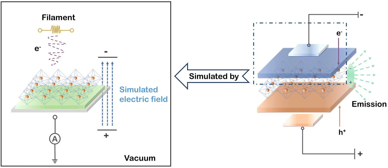 | ||
| Fig. 1 Schematic experimental model of an operating PeLED by the built-in charge neutralizing system in the XPS chamber. | ||
The 3D and reduced-dimensional CsPbBr3 films were prepared for comparison under the same conditions (see Experimental section for details). As displayed in Fig. 2a–f, a new XPS peak of the Pb 4f7/2 orbital located at ∼136.5 eV occurs in the case of PEABr-doped MHP film after electron radiation for 3 h.10,23 As is well known, Pb is an essential element in perovskite unit cells, which directly influences the structural stability of the crystal and photophysical properties. A change of the Pb valence state provides evidence of octahedron unit destruction or crystal transformation. According to previous research, the XPS peak of the Pb signal at ∼136.5 eV can be recognized as metallic Pb0 or Cs4PbBr6.17,24–27 X-ray diffraction (XRD) measurements were performed to obtain structural information of the PEA+-doped MHP film before and after electron radiation (Fig. S2†). The almost identical XRD patterns indicate that no new phase is formed, which confirms that the new XPS signal is derived from Pb0. As is widely recognized, metallic Pb0 is detrimental for carrier transfer and tends to induce severe non-irradiative recombination.24,27 The reduction of Pb2+ has been reported in MAPbI3 perovskite for solar cells as a redox process triggered by illumination or heat, where MA+ refers to a methylamine cation.27 The photogenerated excitons in MAPbI3 are separated into electrons and holes, resulting in Pb2+ reduction and I− oxidation, respectively. Since electron radiation is the only variable in our work, the formation of metallic Pb0 can be ascribed to the reduction reaction induced by electron flow. Interestingly, the total Pb signal maintains a certain intensity, while the N signal decreases, providing strong evidence of N element loss into the vacuum. Hence, we speculate that the decomposition of PEABr, which is the source of N element, provides a great opportunity for Pb2+ reduction.
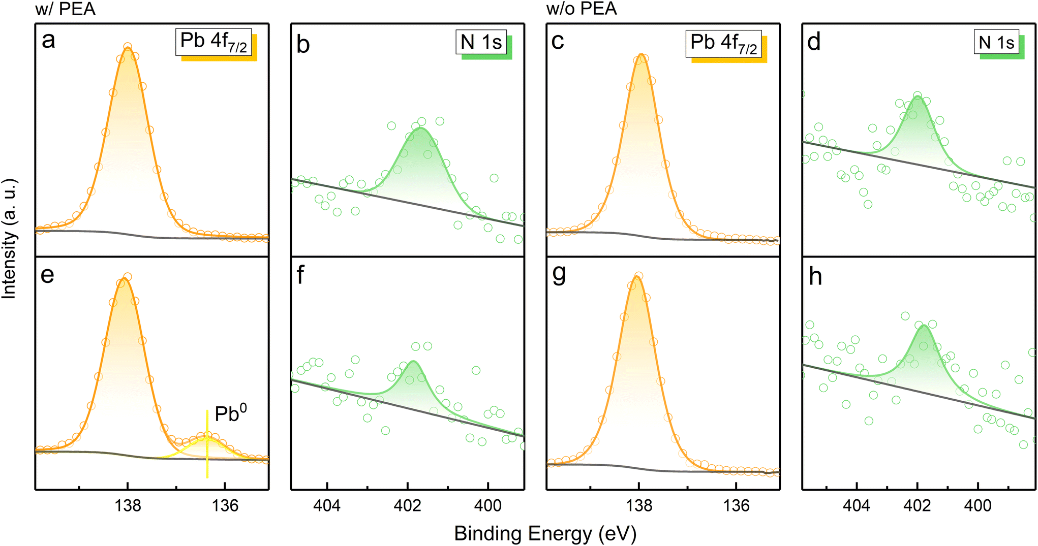 | ||
| Fig. 2 Evolution of the chemical state and element content in 3D and reduced-dimensional CsPbBr3 films. In situ XPS spectra from the orbitals of (a) Pb 4f7/2 and (b) N 1s in perovskite film w/PEA, and (c) Pb 4f7/2 and (d) N 1s in perovskite film w/o PEA before electron radiation; (e) Pb 4f7/2 and (f) N 1s in perovskite film w/PEA, and (g) Pb 4f7/2 and (h) N 1s in perovskite film w/o PEA after electron radiation for 3 h. | ||
The optical properties of PEA+-doped reduced-dimensional MHP film was studied by steady and transient PL measurements (Fig. S3†). A decrease in PL intensity from the low-n phase (n = 3) was observed (as marked by an arrow), along with an obvious red shift of 4 nm in the PL spectrum, which can be attributed to a perovskite recrystallization process. The decomposition of organic spacer PEA+ and the reduction of Pb2+ lead to the associated octahedron exfoliation and decrease in the octahedron layers. However, as the octahedron layers are being destroyed and the n values are becoming smaller, the PL emission should have blue-shifted according to the quantum confinement effect.28,29 Hence, a surface recrystallization process of the low-n phase transferring to the high-n phase under electron radiation possibly exists, which is responsible for the spectral PL red shift. A faster transient PL decay (Fig. S3† inset) is observed for the perovskite films treated by electron radiation, demonstrating the increased defects for non-radiative recombination. Fig. S4† shows the scanning electronic microscopy (SEM) morphology of PEA+-doped MHP film before and after electron radiation. Apparent blurred regions can be observed in the SEM image of pristine PEA+-doped MHP film, which can be attributed to blocked secondary electrons induced by the insulating PEABr accumulation. By contrast, these blurred regions vanish after electron radiation, which represents evidence of the reduced PEA+ content. Moreover, more pinholes appear on the electron-radiated film, probably resulting from N escaping and perovskite recrystallization.
Meanwhile, 3D CsPbBr3 perovskite without PEABr was investigated for comparison. Different from the PEA+-doped perovskite film, no Pb0 XPS signal is observed in the case of the 3D perovskite sample (Fig. 2c and g). Moreover, the 3D perovskite film also gives the N 1s signal, which exhibits no change in the XPS spectra under electron radiation (Fig. 2d and h), probably due to the absorbed nitrogen gas from the glovebox. Considering the distinct differences in the chemical state of Pb and the content of N, it is convincing that the organic spacer PEABr plays an essential role in the reduction of Pb2+.
Considering the ion migration property of perovskite materials,30 an assessment of ion migration is needed. The variation in surface element content was examined by in situ XPS measurements on the PEA+-doped perovskite film to gain more details of the reduction process. Thereinto, Pb atom is assumed as the only unmovable species under an electric field because of its highest activation energy in the perovskite matrix.31 The elemental content ratios were obtained by integrating the peak areas of XPS spectra. The content ratios of perovskite components over Pb element were recorded to evaluate the ion migration occurring during electron radiation. As discussed above, all-inorganic 3D CsPbBr3 film shows excellent electron durability even after 8 h of radiation (Fig. S5†). However, as the radiation time increases, the XPS signal of Pb0 becomes more noticeable in PEA+-doped perovskite film, while the N signal exhibits an opposite evolution (Fig. S6†). Synchronous change demonstrates that Pb2+ reduction and N escape is concomitant. To take a deep look into the underlying process, the evolutional surface element contents are traced. As shown in Fig. 3a, Pb0 content rises with the increasing radiation time in PEA+-doped perovskite film. The content changes of other components in perovskite film are also collected (Fig. 3b) for comparison. The fitted integrated peak areas of XPS spectra are listed in Table S1.† Apparently, the PEA amount shrinks as radiation time increases, which was calculated from the N signal. According to the content ratio of Cs/Pb, we confirm that Cs+ tends to move close to the film surface triggered by electron radiation. An analogy can be obtained for the N escape, indicating that the drive force probably originates from the electric field. The difference is that heavier Cs+ just remains on the surface while the lighter ammonium ion separated from the benzene ring can be pumped into the vacuum. Opposite to the electron flow direction, Br− tends to move down into the perovskite film, resulting in the decrease of the Br/Pb amount ratio. The above ion migration behaviors can verify the effectiveness of our experimental scheme by using a charge neutralizing system to simulate the electric field in a working PeLED.
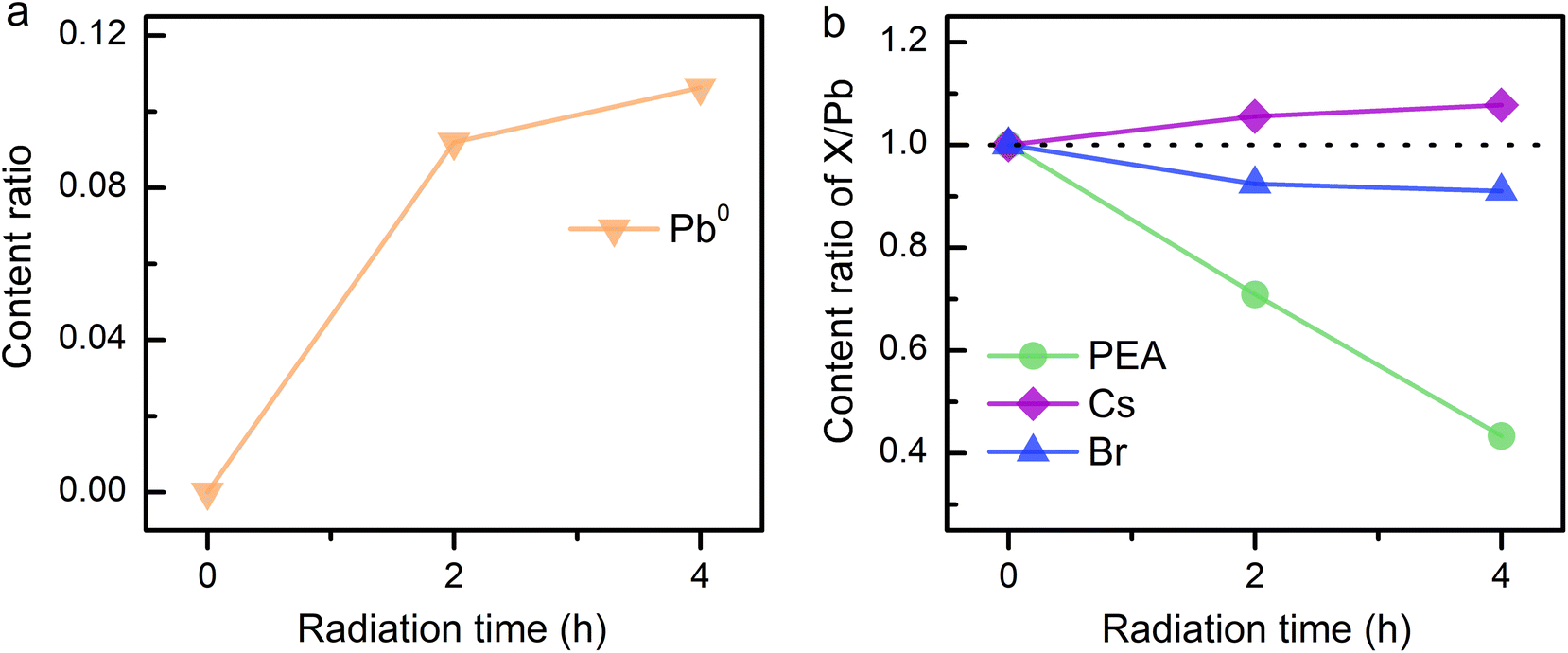 | ||
| Fig. 3 Content change of elements in PEA+-doped CsPbBr3 film. (a) Evolutional content ratios of Pb0. (b) PEA, Cs, and Br to the total Pb with increasing radiation time. | ||
Since the synchronous changes in PEA+ and Pb2+ have been confirmed, pure PEABr and PbBr2 samples were tested by in situ XPS under electron radiation to deduce the detailed process of perovskite degradation. Firstly, the good vacuum stability of PEABr film was proved by an XPS survey scan (Fig. S7a†). As the electron radiation time increases, the XPS signals from the ITO substrate below the PEABr film become stronger, indicating the gradual decomposition process of PEABr molecules (Fig. 4a). As depicted in the inset, the elemental content changes of N and Br exhibit a similar trend as observed in PEA+-doped perovskite film under electron radiation, which further verifies the PEA+ decomposition in perovskite film. In reduced-dimensional perovskite crystals, PEA+ substitutes Cs+ at the same lattice position to arrange the [PbBr6]4− octahedrons to form a layered structure. The decomposition of PEA+ results in the A-site becoming empty, by which the Pb2+ ions near the grain surface become uncoordinated and exposed to the vacuum, providing great opportunity for the reduction reaction under electron radiation. Taking this into consideration, the electron durability of PbBr2 film was also investigated (Fig. 4b–e). The in situ XPS measurement shows an even larger tendency for Pb2+ reduction than that in reduced-dimensional perovskite film under electron radiation. Hence, we can deduce that the loss of A-site cations contributes to the formation of a PbBr2-analogous state, which is prone to be reduced under electron radiation. In addition, a distinct XPS spectral shift of 0.9 eV is observed for both Pb and Br elements, possibly resulting from the unbalanced charge after Pb2+ reduction. Due to the composition migration characteristics of perovskite film, no similar XPS spectral shift is detected. To demonstrate the excellent electron durability of all-inorganic CsPbBr3 film, an in situ XPS measurement on pure CsBr film under electron radiation was performed, indicating no vibration in its content change and chemical state. Accordingly, in inorganic CsPbBr3 film, the electron-stable A-site Cs+ can act as a robust shield for Pb2+ against the electron radiation, thereby suppressing the reduction process. It is noteworthy that a short (∼10 s) contact with air is unavoidable when transferring the perovskite samples from the N2-filled glovebox into the XPS chamber. Given that oxygen and moisture can decompose perovskites, the inorganic CsPbBr3 film was placed in ambient air for 30 min before undertaking XPS measurements. The XPS spectra still undergo no change under electron radiation (Fig. S8†), demonstrating that the short air contact does not affect the validity of our research.
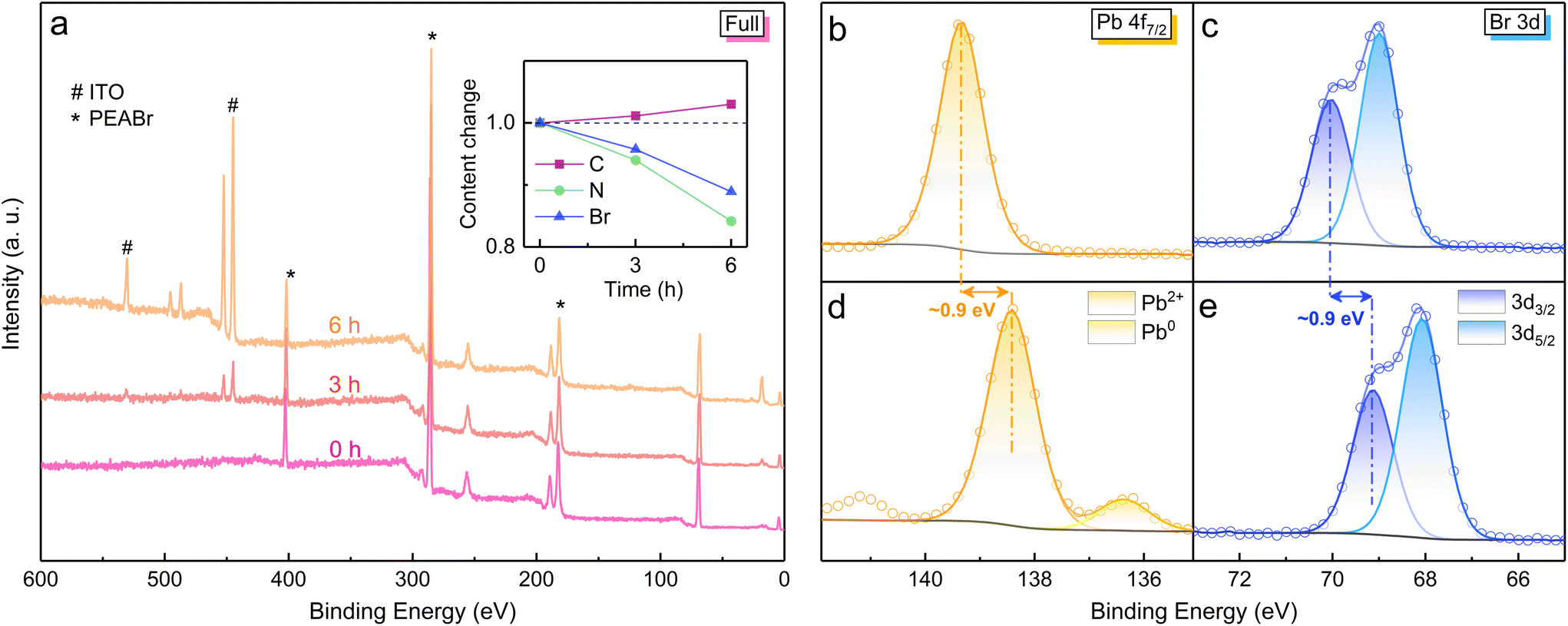 | ||
| Fig. 4 Variations in elemental contents and chemical states. (a) In situ survey scan of PEABr film on ITO substrate with increasing radiation time. The inset shows elemental content changes with respect to their initial values. In situ XPS spectra from the orbitals of Pb 4f7/2 and Br 3d before (b, c) and after (d, e) electron radiation for 3 h. | ||
Furthermore, the formamidine (FA+)-based 3D and PEA+-doped reduced-dimensional perovskites were also studied to prove the universality of our findings. The XPS spectra of Pb0 and N from PEA+ display the analogical variation trend under electron radiation as discussed for the reduced-dimensional Cs-based perovskite (Fig. 5a and b). Moreover, the content evolution of Pb and PEA components corresponds to the phenomena of Pb2+ reduction and PEA decomposition (Fig. 5c and d), respectively. The fitted peak areas of XPS spectra are listed in Table S2.† In addition, the electron durability of the 3D FAPbBr3 film is as excellent as the 3D CsPbBr3 film (Fig. S9†). Therefore, it is believed that PEA+-doped reduced-dimensional perovskites generally feature degraded electron durability compared with their 3D counterparts.
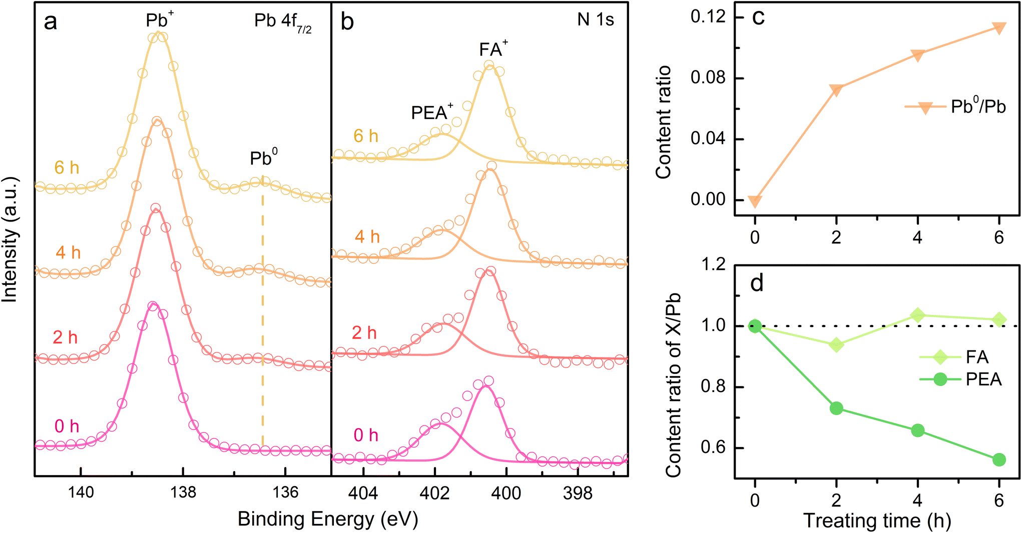 | ||
| Fig. 5 Evolution of the chemical state and element content in PEA+-doped FAPbBr3 film. In situ time-resolved XPS spectra from the orbitals of (a) Pb 4f7/2 and (b) N 1s in PEA and FA. Evolutional content ratio of (c) Pb0 and (d) FA and PEA to the total Pb with increasing radiation time. | ||
Based on the above results and discussions, we are able to present the decomposition mechanism of PEA+-doped reduced-dimensional perovskite, as schematically depicted in Fig. 6. In the layered perovskite structure, as the electron beam erodes the spacing region near perovskite octahedrons, the positive charge centers (–NH3+) of PEA+ escape into the vacuum, leaving unmovable and uncharged phenethyl in place. The main driving force of –NH3+ is the electric field induced by electron radiation. The breakages of PEA+ cations make the surface [PbBr6]4− octahedrons exposed to electron radiation, marked as the orange crystal region in the diagram. Persistently lacking A-site cations make the surface electronic configuration prone to capturing electrons, leading to the reduction process from Pb2+ to metallic Pb0. Considering the photophysical changes induced by electron radiation, the component migration forced by the electric field further contributes to the surface crystal rearrangement of layered perovskite structures from the low-n phase to the high-n phase. Moreover, we speculate that extra crystal defects may occur during this spontaneous process. Consequently, an obvious spectral red shift and reduced exciton decay lifetime were demonstrated for the PEA+-doped reduced-dimensional perovskite. Therefore, the vulnerability of the organic spacers can be a critical factor for the degraded electron durability of reduced-dimensional perovskites. Toward long-term practical device operation, the layered perovskite structure may be fully depleted, leaving growing 3D crystals with masses of defects. Such an unfavorable transformation would result in devastating damage in the operational stability of reduced-dimensional PeLEDs.
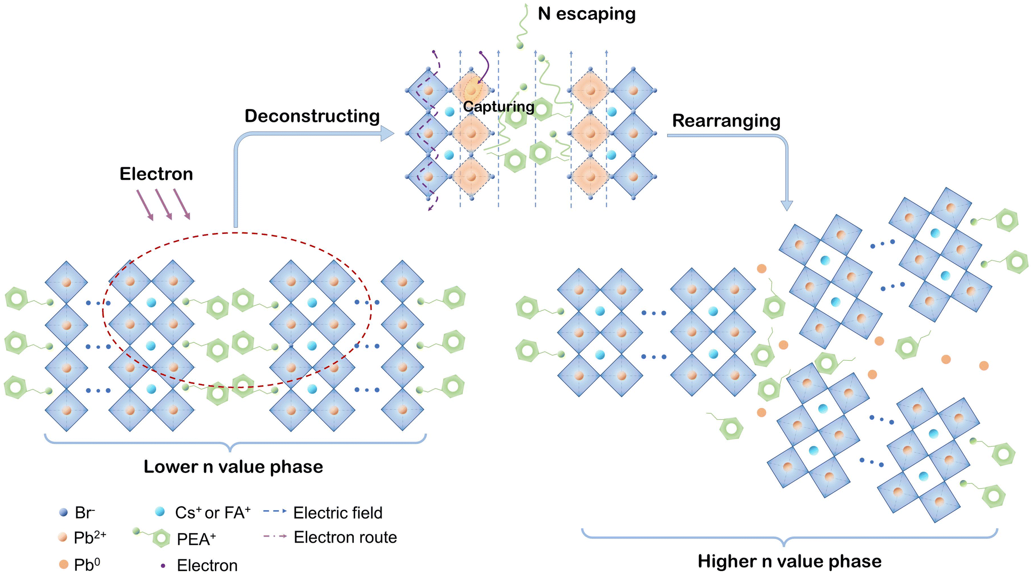 | ||
| Fig. 6 Schematic mechanism diagram of the degraded electron durability in PEA+-doped reduced-dimensional perovskites. | ||
4. Conclusion
In summary, the electron durability of PEA+-doped perovskites has been investigated to unveil the critical degradation process in reduced-dimensional PeLEDs under continuous operation. A rational and feasible research scheme is proposed by employing a built-in charge neutralization system to simulate practical device operation for in situ XPS measurements in ultra-high vacuum. In this way, the metallic Pb atom along with spacer decomposition is observed under electron radiation. We demonstrate that the current-induced PEA+ loss makes the nearby Pb2+ prone to capturing electrons, thereby triggering an unwanted reduction from Pb2+ to Pb0, which represents a universal drawback in the PEA+-doped reduced-dimensional perovskites. It is further deduced that the fractured layered perovskite tends to undergo crystal rearrangement from the low-n phase to the high-n phase. The irreversible influence of electron flow on the layered perovskite structures is detrimental to the long-term operational stability of the mainstream PEA+-doped PeLEDs. Our findings unravel the critical drawback of reduced-dimensional perovskites and provide potential guidance for upgrading organic spacers.Author contributions
Jian-Xin Tang designed the experiments. Yu Lu and Wei Zhou carried out the experiments assisted by Kong-chao Shen, while Yu Lu analyzed the data. Jian-Xin Tang and Kong-chao Shen provided guidance during the experiments and analysis. All authors discussed the results. Yu Lu and Yang Shen wrote the manuscript with contributions from all authors.Conflicts of interest
There are no conflicts to declare.Acknowledgements
The authors acknowledge the financial support from the National Key R&D Program of China (No. 2022YFE0108900), the Science and Technology Development Fund (FDCT), Macau SAR (No. 0018/2022/A1), the National Natural Science Foundation of China (No. 62274117, 62075061), the Science and Technology Innovation Plan of Shanghai Science and Technology Commission (No. 22520760600), the Jiangsu Provincial Department of Science and Technology (No. BZ2022054), and the Collaborative Innovation Center of Suzhou Nano Science & Technology.References
- Z.-K. Tan, R. S. Moghaddam, M. L. Lai, P. Docampo, R. Higler, F. Deschler, M. Price, A. Sadhanala, L. M. Pazos, D. Credgington, F. Hanusch, T. Bein, H. J. Snaith and R. H. Friend, Nat. Nanotechnol., 2014, 9, 687–692 CrossRef CAS PubMed
.
- V. A. Hintermayr, A. F. Richter, F. Ehrat, M. Doblinger, W. Vanderlinden, J. A. Sichert, Y. Tong, L. Polavarapu, J. Feldmann and A. S. Urban, Adv. Mater., 2016, 28, 9478–9485 CrossRef CAS PubMed
- Z. Chu, X. Chu, Y. Zhao, Q. Ye, J. Jiang, X. Zhang and J. You, Small Struct., 2021, 2, 2000133 CrossRef CAS
- Y. Shen, J.-K. Wang, Y.-Q. Li, K.-C. Shen, Z.-H. Su, L. Chen, M.-L. Guo, X.-Y. Cai, F.-M. Xie, X.-Y. Qian, X. Gao, I. S. Zhidkov and J.-X. Tang, Adv. Sci., 2021, 8, 2102213 CrossRef CAS PubMed
- Z. Liu, W. Qiu, X. Peng, G. Sun, X. Liu, D. Liu, Z. Li, F. He, C. Shen, Q. Gu, F. Ma, H.-L. Yip, L. Hou, Z. Qi and S.-J. Su, Adv. Mater., 2021, 33, 2103268 CrossRef CAS PubMed
- Z. Yuan, Y. Miao, Z. Hu, W. Xu, C. Kuang, K. Pan, P. Liu, J. Lai, B. Sun, J. Wang, S. Bai and F. Gao, Nat. Commun., 2019, 10, 2818 CrossRef PubMed
- X. K. Liu, W. Xu, S. Bai, Y. Jin, J. Wang, R. H. Friend and F. Gao, Nat. Mater., 2021, 20, 10–21 CrossRef CAS PubMed
- G. Xing, B. Wu, X. Wu, M. Li, B. Du, Q. Wei, J. Guo, E. K. Yeow, T. C. Sum and W. Huang, Nat. Commun., 2017, 8, 14558 CrossRef CAS PubMed
- Y.-K. Wang, F. Yuan, Y. Dong, J.-Y. Li, A. Johnston, B. Chen, M. I. Saidaminov, C. Zhou, X. Zheng, Y. Hou, K. Bertens, H. Ebe, D. Ma, Z. Deng, S. Yuan, R. Chen, L. K. Sagar, J. Liu, J. Fan, P. Li, X. Li, Y. Gao, M.-K. Fung, Z.-H. Lu, O. M. Bakr, L.-S. Liao and E. H. Sargent, Angew. Chem., Int. Ed., 2021, 60, 16164–16170 CrossRef CAS PubMed
- Y. Shen, L. P. Cheng, Y. Q. Li, W. Li, J. D. Chen, S. T. Lee and J. X. Tang, Adv. Mater., 2019, 31, 1901517 CrossRef PubMed
- Z. Chu, Q. Ye, Y. Zhao, F. Ma, Z. Yin, X. Zhang and J. You, Adv. Mater., 2021, 33, 2007169 CrossRef CAS PubMed
- T. Chiba, Y. Hayashi, H. Ebe, K. Hoshi, J. Sato, S. Sato, Y.-J. Pu, S. Ohisa and J. Kido, Nat. Photonics, 2018, 12, 681–687 CrossRef CAS
- L. Mao, C. C. Stoumpos and M. G. Kanatzidis, J. Am. Chem. Soc., 2019, 141, 1171–1190 CrossRef CAS PubMed
- Z. Huang, A. H. Proppe, H. Tan, M. I. Saidaminov, F. Tan, A. Mei, C.-S. Tan, M. Wei, Y. Hou, H. Han, S. O. Kelley and E. H. Sargent, ACS Energy Lett., 2019, 4, 1521–1527 CrossRef CAS
- Y. Zhang, J. Wen, Z. Xu, D. Liu, T. Yang, T. Niu, T. Luo, J. Lu, J. Fang, X. Chang, S. Jin, K. Zhao and S. F. Liu, Adv. Sci., 2021, 8, e2001433 CrossRef PubMed
- K. Ho, M. Wei, E. H. Sargent and G. C. Walker, ACS Energy Lett., 2021, 6, 934–940 CrossRef CAS
- L. Lu, K. C. Shen, J. Wang, Z. Su, Y. Li, L. Chen, Y. Luo, F. Song, X. Gao and J. X. Tang, ACS Appl. Mater. Interfaces, 2020, 12, 42369–42377 CrossRef CAS PubMed
- C. Kuang, Z. Hu, Z. Yuan, K. Wen, J. Qing, L. Kobera, S. Abbrent, J. Brus, C. Yin, H. Wang, W. Xu, J. Wang, S. Bai and F. Gao, Joule, 2021, 5, 618–630 CrossRef CAS
- T.-H. Han, J.-W. Lee, C. Choi, S. Tan, C. Lee, Y. Zhao, Z. Dai, N. De Marco, S.-J. Lee, S.-H. Bae, Y. Yuan, H. M. Lee, Y. Huang and Y. Yang, Nat. Commun., 2019, 10, 520 CrossRef CAS PubMed
- Y. Liu, A. V. Ievlev, N. Borodinov, M. Lorenz, K. Xiao, M. Ahmadi, B. Hu, S. V. Kalinin and O. S. Ovchinnikova, Adv. Funct. Mater., 2021, 31, 2008777 CrossRef CAS
- P. Teng, S. Reichert, W. Xu, S.-C. Yang, F. Fu, Y. Zou, C. Yin, C. Bao, M. Karlsson, X. Liu, J. Qin, T. Yu, W. Tress, Y. Yang, B. Sun, C. Deibel and F. Gao, Matter, 2021, 4, 3710–3724 CrossRef CAS
- J. Hu, P. Chen, D. Luo, D. Wang, N. Chen, S. Yang, Z. Fu, M. Yu, L. Li, R. Zhu and Z.-H. Lu, Commun. Mater., 2022, 3, 39 CrossRef CAS
- M.-L. Guo, Y. Lu, X.-Y. Cai, Y. Shen, X.-Y. Qian, H. Ren, Y.-Q. Li, W.-J. Wang and J.-X. Tang, J. Mater. Chem. C, 2022, 10, 2998–3005 RSC
- Z. Guo, S. Zhao, N. Shibayama, A. Kumar Jena, I. Takei and T. Miyasaka, Adv. Funct. Mater., 2022, 202207554 Search PubMed
- K. Lin, C. Yan, R. P. Sabatini, W. Feng, J. Lu, K. Liu, D. Ma, Y. Shen, Y. Zhao, M. Li, C. Tian, L. Xie, E. H. Sargent and Z. Wei, Adv. Funct. Mater., 2022, 32, 2200350 CrossRef CAS
- J. Holovský, A. Peter Amalathas, L. Landová, B. Dzurňák, B. Conrad, M. Ledinský, Z. Hájková, O. Pop-Georgievski, J. Svoboda, T. C.-J. Yang and Q. Jeangros, ACS Energy Lett., 2019, 4, 3011–3017 CrossRef
- E. J. Juarez-Perez, L. K. Ono, M. Maeda, Y. Jiang, Z. Hawash and Y. Qi, J. Mater. Chem. A, 2018, 6, 9604–9612 RSC
- L. Zhang, C. Sun, T. He, Y. Jiang, J. Wei, Y. Huang and M. Yuan, Light: Sci. Appl., 2021, 10, 61 CrossRef CAS PubMed
- Z. Chu, Y. Zhao, F. Ma, C. X. Zhang, H. Deng, F. Gao, Q. Ye, J. Meng, Z. Yin, X. Zhang and J. You, Nat. Commun., 2020, 11, 4165 CrossRef CAS PubMed
- J. M. Azpiroz, E. Mosconi, J. Bisquert and F. De Angelis, Energy Environ. Sci., 2015, 8, 2118–2127 RSC
- C. Eames, J. M. Frost, P. R. F. Barnes, B. C. O'Regan, A. Walsh and M. S. Islam, Nat. Commun., 2015, 6, 7497 CrossRef CAS PubMed
Footnote |
| † Electronic supplementary information (ESI) available. See DOI: https://doi.org/10.1039/d2nr06635a |
| This journal is © The Royal Society of Chemistry 2023 |