
 Open Access Article
 This Open Access Article is licensed under a
 Creative Commons Attribution 3.0 Unported Licence
Photosensitisation of inkjet printed graphene with stable all-inorganic perovskite nanocrystals†
Jonathan S.
Austin‡
 a,
Nathan D.
Cottam‡
b,
Chengxi
Zhang‡
c,
Feiran
Wang
a,
Jonathan H.
Gosling
ab,
Oliver
Nelson-Dummet
a,
Tyler S. S.
James
b,
Peter H.
Beton
b,
Gustavo F.
Trindade
d,
Yundong
Zhou
d,
Christopher J.
Tuck
a,
Richard
Hague
a,
Oleg
Makarovsky
b and
Lyudmila
Turyanska
*a
a,
Nathan D.
Cottam‡
b,
Chengxi
Zhang‡
c,
Feiran
Wang
a,
Jonathan H.
Gosling
ab,
Oliver
Nelson-Dummet
a,
Tyler S. S.
James
b,
Peter H.
Beton
b,
Gustavo F.
Trindade
d,
Yundong
Zhou
d,
Christopher J.
Tuck
a,
Richard
Hague
a,
Oleg
Makarovsky
b and
Lyudmila
Turyanska
*a
aCentre for Additive Manufacturing, Faculty of Engineering, University of Nottingham, Jubilee Campus, Nottingham, NG8 1BB, UK. E-mail: Lyudmila.Turyanska@nottingham.ac.uk
bSchool of Physics and Astronomy, University of Nottingham, Nottingham, NG7 2RD, UK
cKey Laboratory of Advanced Display and System Applications, Shanghai University, 149 Yanchang Road, 200072, China
dNational Physical Laboratory, Teddington, Middlesex TW11 0LW, UK
First published on 23rd December 2022
Abstract
All-inorganic perovskite nanocrystals (NCs) with enhanced environmental stability are of particular interest for optoelectronic applications. Here we report on the formulation of CsPbX3 (X is Br or I) inks for inkjet deposition and utilise these NCs as photosensitive layers in graphene photodetectors, including those based on single layer graphene (SLG) as well as inkjet-printed graphene (iGr) devices. The performance of these photodetectors strongly depends on the device structure, geometry and the fabrication process. We achieve a high photoresponsivity, R > 106 A W−1 in the visible wavelength range and a spectral response controlled by the halide content of the perovskite NC ink. By utilising perovskite NCs, iGr and gold nanoparticle inks, we demonstrate a fully inkjet-printed photodetector with R ≈ 20 A W−1, which is the highest value reported to date for this type of device. The performance of the perovskite/graphene photodetectors is explained by transfer of photo-generated charge carriers from the perovskite NCs into graphene and charge transport through the iGr network. The perovskite ink developed here enabled realisation of stable and sensitive graphene-based photon detectors. Compatibility of inkjet deposition with conventional Si-technologies and with flexible substrates combined with high degree of design freedom provided by inkjet deposition offers opportunities for partially and fully printed optoelectronic devices for applications ranging from electronics to environmental sciences.
Introduction
Over the past decade the photoresponsivity of photodetectors based on low-dimensional materials has improved drastically due to materials innovation.1–3 However, these high-performance devices typically require bespoke fabrication techniques and are yet to reach commercial viability.1,2 Additive manufacturing (AM), specifically inkjet printing, has the significance of offering a promising route for large scale, industrial style fabrication of devices incorporating nanomaterials such as graphene,4,5 perovskites6–10 and quantum dots.11–13 Recently, fully inkjet manufactured organic photon detectors were demonstrated on flexible substrates14 and rigid substrates with photoresponsivity, R up to ∼104 A W−1.15 Fully printed graphene/CH3NH3PbClX−3I3/graphene devices demonstrated lower responsivity R ∼ 10−1 A W−1.16 However, organic devices tend to have a slow response17 and poor long-term stability.18Photosensitisation of graphene by surface decoration with inorganic nanomaterials, such as 2D black phosphorus19 and colloidal quantum dots (e.g. ZnO,11 HgTe,12 and PbS13), enables a high degree of tunability of the spectral sensitivity range by size and composition of the nanomaterial. Among low-dimensional materials, perovskite nanocrystals (NCs) are of particular interest for photodetection applications, owing to their high absorption cross-sections, long carrier diffusion lengths, and tuneable optical properties.20 Recently, lead halide-based inks (PbX2, X = Br or I),21 hybrid MAPbBr3,6,7 MAPbX3,8 CH3NH3PbI3,9 and (CH3(CH2)3NH3)2(CH3NH3)n−1PbnI3n+110 perovskites were inkjet-deposited to produce photodetectors with photoresponsivity up to ∼10 A W−1.7 Compatibility of AM techniques with different substrates allows the integration of these new materials with conventional silicon based technologies,12 as well as the fabrication of photodetectors on flexible substrates, such as polyethylene terephthalate and polyimide.6,10 Stable photoresponsivity of up to ∼1 A W−1 was achieved after 15![[thin space (1/6-em)]](https://www.rsc.org/images/entities/char_2009.gif) 000 bending cycles with MAPbBr3 perovskites.6 Recently, significant interest focussed on all-inorganic lead halide perovskites CsPbX3 due to their improved environmental stability,22 however their development for inkjet deposition is still in its infancy, with few reported examples, such as inkjet deposition of CsPbX3 for soft X-ray detection.23,24 Enhanced stability of these perovskites and their integration with AM technologies is yet to be fully exploited for fabrication of optoelectronic devices.
000 bending cycles with MAPbBr3 perovskites.6 Recently, significant interest focussed on all-inorganic lead halide perovskites CsPbX3 due to their improved environmental stability,22 however their development for inkjet deposition is still in its infancy, with few reported examples, such as inkjet deposition of CsPbX3 for soft X-ray detection.23,24 Enhanced stability of these perovskites and their integration with AM technologies is yet to be fully exploited for fabrication of optoelectronic devices.
Here we report a novel formulation of all-inorganic CsPbX3 NC inks for inkjet printing and demonstrate high precision fabrication of complex photoluminescent patterns, including deposition on flexible substrates. We explore different approaches to fabricate perovskite/graphene photodetectors, both combining fabrication of conventional graphene/SiO2/Si with inkjet and fully inkjet deposited heterostructures, and propose a qualitative model that links together their electronic (conductivity, carrier mobility) and optoelectronic (photosensitivity, response time) properties. We explore the deposition of these photosensitive layers onto chemical vapour deposition (CVD) grown single layer graphene (SLG), as well as inkjet deposited graphene (iGr) films to produce photodetectors with high responsivities up to 106 A W−1, tuneable in the VIS–UV range. By inkjet deposition of electrodes (Au nanoparticle inks), graphene, and perovskites we demonstrate a fully-printed CsPb(Br/I)3/iGr photon detector, with a maximum responsivity of about 20 A W−1. The performance of these devices is analysed and explained using modelling of charge transport through functionalised graphene and graphene networks. The compatibility of inkjet deposition with conventional Si-based substrates and devices, and with flexible substrates could enable numerous opportunities, from displays to optoelectronic devices.
Results and discussion
CsPbX3 (X = Br or Br/I mix) perovskite NCs were synthesised using the hot-injection method22 and were used to formulate inks for inkjet printing (Fig. 1a). The NCs had an average size of 11 ± 1 nm and were hexagonal in shape with high crystallinity as expected for the used synthesis method,25 which leads to the formation of polyhedral perovskite nanocrystals due to ammonium ions stabilization of different crystal facets. A lattice spacing of 0.41 ± 0.02 nm was measured from HRTEM images, which corresponds to (110) plane of cubic CsPbBr326 (Fig. 1b and ESI, SI1, Fig. S1†). These NCs are stable with respect to their optical properties for a period of at least 2 months (ESI, SI1 and Fig. S2†). To formulate the inks, the NCs were added to a mixture of hexane, cyclohexanone, and terpineol (1:3:1 v/v) at a concentration of 5 mg ml−1. The composition of the ink was optimised to achieve the viscosity of 1.53 mPa s, surface tension of 37.8 mN m−1, and density of 1.33 g cm−3, which renders it suitable for inkjet deposition. To suppress the coffee ring effect, the high boiling point solvents terpineol and cyclohexanone, and the low boiling point solvent hexane are included together in the ink27,28 and the substrate temperature was set to 60 °C during printing. The inks were deposited using a 20 μm drop spacing in an inert N2 atmosphere to avoid NC oxidation. Printed perovskite NC films were dried on the heated print-bed at T = 60 °C for 30 minutes. Two types of perovskite NCs with different halogen contents were formulated into inks as described above: green CsPbBr3 and red CsPb(Br/I)3 NCs (Fig. 1c and d), which have photoluminescence (PL) emissions centred at 515 nm and 625 nm, respectively (Fig. 1d). Both inks demonstrated bright fluorescence under UV illumination both before and after deposition and drying (Fig. 1a, c and d).
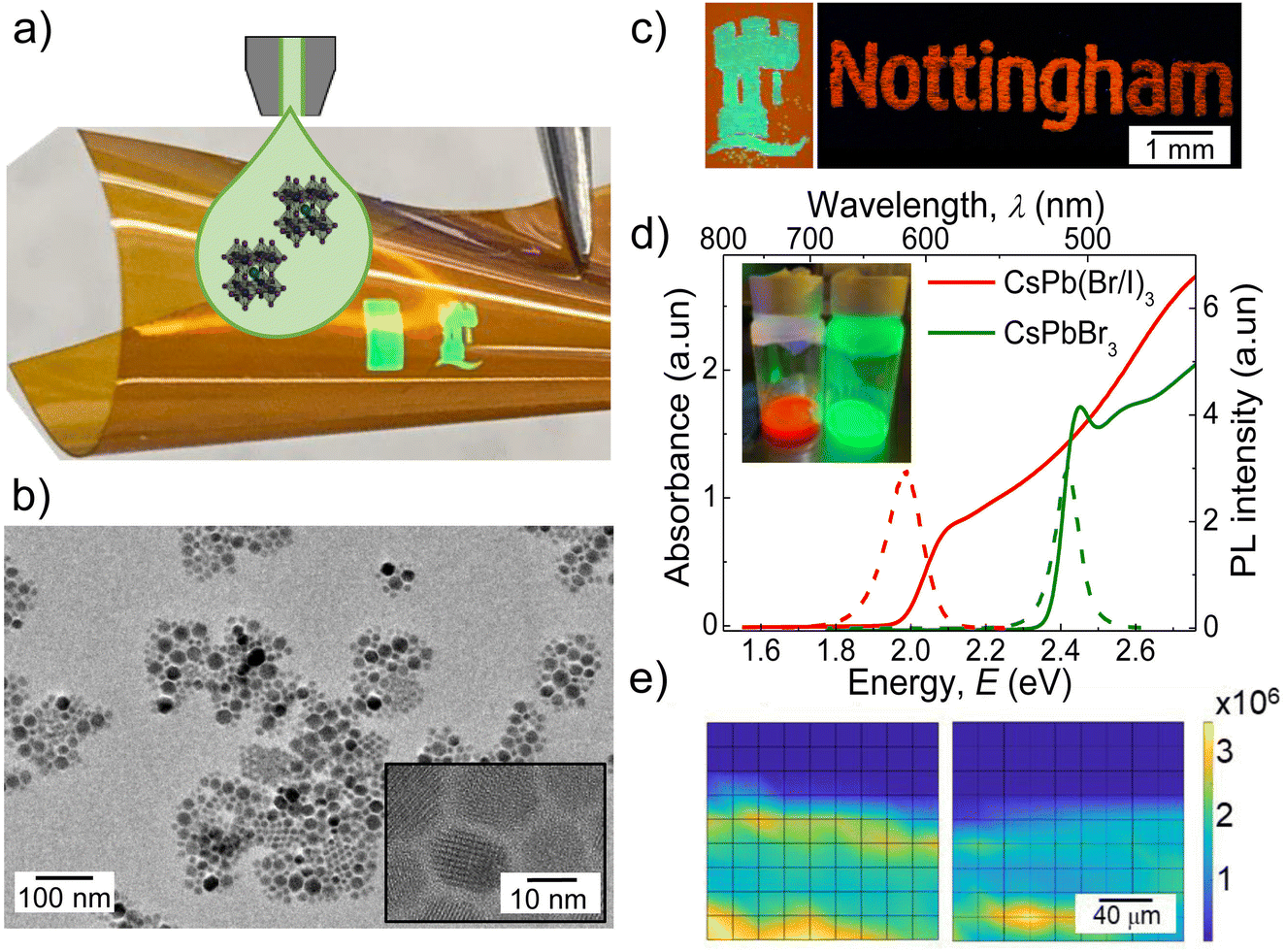 | ||
| Fig. 1 (a) Scheme for 5 mg ml−1 CsPbX3 (X = Br, I, or mixed) perovskite NC ink formulation for inkjet printing (solvents (vol): 20% hexane, 60% cyclohexanone, 20% terpineol) with optical image of green pattern on Kapton undergoing bending with bright fluorescence under UV (λex = 365 nm) illumination. (b) TEM and HRTEM (inset) images of CsPbBr3 NCs. (c) Optical image of printed perovskite NC films with green CsPbBr3 on Kapton and red CsPb(Br/I)3 NCs on Si/SiO2, both under UV illumination (λex = 365 nm). (d) Photoluminescence spectra of printed films (dashed lines) and absorption spectra of inks (solid lines) for green CsPbBr3 and red CsPb(Br/I)3 NCs. (e) Map of PL emission intensity for 1 printed layer (left) and 2 printed layer (right) CsPbBr3 NC films on Si/SiO2 substrate. | ||
We note that uniform films are formed using a single printed layer. Only a factor of 2 difference between the maximum and minimum PL intensity was recorded on PL maps of these samples (Fig. 1e) and is attributed to the surface roughness, which correlates with the printed line spacing. The surface roughness is reduced with increasing number of layers and more uniform maps of PL intensity are recorded. Importantly, thermal annealing, which is typically used as post deposition process (T = 100 °C), has a negligible effect on the film morphology and optical properties (see ESI, SI2 and Fig. S3†). Atomic force microscopy (AFM) images revealed that CsPbBr3 films with 5 printed layers had a thickness of ∼20 nm, with a surface roughness of ∼5 nm (see ESI, SI3 and Fig. S4†).
CsPbBr3 and CsPb(Br/I)3 NCs were deposited onto a CVD grown graphene field effect transistor (FET), SLG/SiO2/Si, by inkjet printing to fabricate CsPb(Br/I)3/SLG and CsPbBr3/SLG devices (Fig. 2a). The gate voltage, Vg, dependence of SLG resistivity before and after deposition of CsPb(Br/I)3 NCs revealed a large hysteresis when Vg was swept from −50 V to +50 V and then back to −50 V with a sweep rate of 0.1 V s−1 (Fig. 2a). The observed hysteresis of the ρ(Vg) dependence is due to slow charging of the perovskite NCs.2,29 This was accompanied by a shift of the position of the Dirac point from +11 V to 0 V, thus indicating n-type doping of the SLG by CsPb(Br/I)3 NCs. Similar n-type doping of SLG has previously been observed on SLG functionalised with CsPbI3 NCs, due to the donor nature of CsPbX3 NCs.2
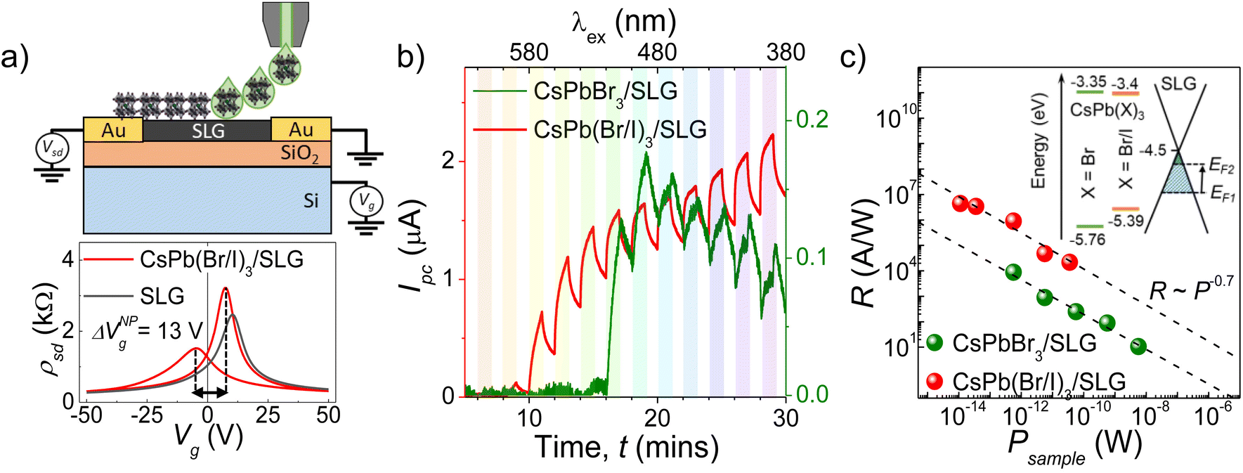 | ||
| Fig. 2 (a) Schematic of deposition of all-inorganic perovskite NCs via inkjet printing on a single layer graphene (SLG) device (top). The dependence of SLG resistivity, ρsd, on applied gate voltage, Vg, during forward and reverse sweeps, before (black curve) and after (red curve) the inkjet-printed deposition of CsPb(Br/I)3 NCs (bottom). Vg is swept from −50 V to +50 V and then back to −50 V (Vsd = 5 mV, sweep rate = 0.1 V s−1). (b) Dependence of photocurrent, Ipc, on the wavelength of incident light for the CsPb(Br/I)3/SLG device (P ∼ 0.03 W m−2, Vsd = 10 mV) and the CsPbBr3/SLG device (P ∼ 0.3 W m−2, Vsd = 5 mV). Shaded regions correspond to light on regime (c) photoresponsivity, R, of the same two devices as a function of illumination power measured after 1 minute illumination with λex = 405 nm exposure (Vsd = 10 mV, Vg = 0 V). Inset: energy band diagram comparing CsPbBr3 NCs, CsPb(Br/I)3 NCs, and SLG. EF1 and EF2 denote the Fermi energy of the SLG device before (−4.6 eV) and after (−4.54 eV) CsPb(Br/I)3 deposition, respectively. | ||
The electron and hole field-effect mobilities of the SLG device before NC deposition were calculated at the point of the highest slope of σ(Vg) (highest value of μFE) for both electrons and holes using the method reported in29,30 (see Methods section). For pristine SLG, μe = 0.70 m2 V−1·s−1 and μh = 0.55 m2 V−1·s−1, respectively. After deposition of CsPb(Br/I)3 NCs, the mobilities decreased to μe = 0.53 m2 V−1·s−1 and μh = 0.40 m2 V−1·s−1 during forward voltage sweeps (−50 V to +50 V) and increased to μe = 0.73 m2 V−1·s−1 and μh = 0.64 m2 V−1·s−1 during backward voltage sweeps (+50 V to −50 V) (see ESI, SI3 and Fig. S5†). Dependence of the field effect mobility on the direction of the Vg sweep can be explained using slow charge dynamics in the CsPbX3/SLG devices.2 The Vg position of the Dirac point of the CsPbBr3/SLG device was also shifted to the left, consistent with n-type doping, as discussed above. A small increase in electron mobility and decrease in hole mobility was observed in the CsPbBr3/SLG device from μe = 0.33 m2 V−1·s−1 and μh = 0.53 m2 V−1·s−1 before NC deposition to μe = 0.38 m2 V−1·s−1 and μh = 0.36 m2 V−1·s−1 after NC deposition (see ESI, SI3 and Fig. S5†). The difference between the devices decorated with CsPb(Br/I)3 and CsPb(Br)3 is likely due to the differences in the properties of the pristine graphene before deposition.
In the CsPbX3/SLG devices, the onset of photoresponse was observed at an excitation wavelength, λex = 600 nm for CsPb(Br/I)3 and λex = 520 nm for CsPbBr3 (Fig. 2b), which is consistent with their respective absorption spectra (see ESI, SI4 and Fig. S7†). After illumination, the electrical properties of the devices recover to ∼90% of the original value in about a minute, however the full recovery can take up to several hours for large incident illumination powers (see ESI, SI3 and Fig. S5†), which is likely due to the charge trapping on NC surface defects and slow charge dynamic.29 For both devices, the relationship between incident light power, P, and the responsivity, R, follows R ∼ P−0.7 (Fig. 2c), similar to the R(P) previously reported for SLG decorated with CsPbI3 NCs.2 A much greater maximum photoresponse was observed for the CsPb(Br/I)3 device (R = 4 × 10⁶ A W−1) than by the CsPbBr3 device (R = 7 × 10³ A W−1), with excitation and relaxation response times of τrise ∼ 2 s and τfall ∼ 6 s (see ESI, SI3 and Fig. S5†). The difference in photoresponsivity of the photodetectors decorated with different perovskite NCs is due to the NC composition, which affects their absorption (Fig. 1d) and energy level alignment with SLG for charge transfer (inset in Fig. 2c). Since higher levels of absorptions at the used excitation energy (405 nm) and longer lifetimes of photoexcited trapped charges are observed for mixed halide CsPb(Br/I)3 NCs, these devices have higher photoresponsivity compared to CsPbBr3 NC decorated devices. The device performance was stable for a period of up to 2 weeks. (ESI, SI3 and Fig. S6†).
The next step towards fully printed photodetectors was to replace the CVD grown SLG with an inkjet-printed graphene (iGr) current channel. A single droplet of iGr ink was deposited onto a Si/SiO2 FET between two pre-patterned gold contacts separated by a 20 μm gap. Perovskite CsPb(Br/I)3 NCs were deposited onto iGr by drop-casting (Fig. 3a). The conductivity, σsd, of this CsPb(Br/I)3/iGr device as a function of gate voltage, Vg, showed a shift in the Dirac point from Vg ∼ 60 V for pristine graphene to Vg ∼ 50 V after (Fig. 3b) for NC functionalised device, indicating n-type doping, similar to that previously observed for the CsPbX3/SLG devices (Fig. 2a). The hole mobility μh = 3 cm2V−1·s−1 was measured for both pristine iGr and CsPb(Br/I)3/iGr devices. However, after deposition of the perovskite NCs the conductivity of the device decreased by ∼7% across the whole range of the applied Vg. Similar change of the conductivity, without shift of the Dirac point or change of mobility, was observed for iGr samples with different thickness (i.e. 1, 2 or 3 droplets printed on top of each other). We ascribe the reduction of the conductivity after the NC deposition to the intermixing of the NCs and iGr, leading to the reduction of the effective layer thickness. The value of mobility and the hysteresis of the σsd(Vg) dependence observed for pristine iGr device (Fig. 3b) are not affected by the surface deposition of CsPb(Br/I)3.
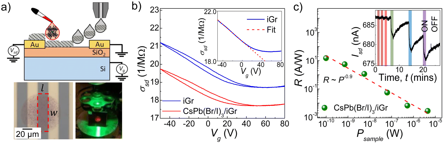 | ||
| Fig. 3 (a) Schematic showing inkjet deposition of iGr and drop-cast CsPb(Br/I)3 to fabricate CsPb(Br/I)3/iGr photodetector (top). Image of iGr droplet printed on Si/SiO2 substrate with pre-deposited gold electrodes spaced by 20 μm gaps (left) and photograph of device after CsPb(Br/I)3 NCs were drop-cast on top, displaying red fluorescence under excitation with λex = 520 nm (right). (b) Conductivity of the iGr device before (blue curve) and after (red curve) drop-cast deposition of CsPb(Br/I)3 NCs (Vsd = 10 mV). Inset: Gate voltage dependence of iGr conductivity (Vsd = 10 mV) and linear fit for field effect model mobility calculation, giving a hole mobility, μh, of 3 cm2 V−1 s−1. (c) Photoresponsivity, R, of CsPb(Br/I)3/iGr photodetector as a function of the power on the sample (λex = 520 nm, Vsd = 10 mV). Inset: temporal response of device under ON/OFF illumination with different wavelength excitation of 1060 nm, 808 nm, 635 nm, 520 nm, 450 nm, and 405 nm (P = 560 W m−2, Vsd = 10 mV, Vg = 0 V). | ||
The photoresponsivity threshold of the CsPb(Br/I)3/iGr device is observed at ∼600 nm (see ESI, SI5 and Fig. S8†), similar to the responsivity threshold observed in the CsPb(Br/I)3/SLG device. The relationship between responsivity and incident power for the CsPb(Br/I)3/iGr device followed R ∼ P−0.5 dependence with a maximum responsivity of 101 A W−1 and a response time constant of τrise = 6 s (inset in Fig. 3c). Note, high photoresponsivity in CsPbX3/graphene photodetectors is proportional to the ratio between perovskite NC charge trapping time, τtrap, and electron transport time, τe ∼1/μ, i.e. the time it takes an electron to pass through the device, R ∼ τtrap/τe.31 Our iGr devices demonstrate field effect mobility, μFE ≈3 cm2 V−1·s−1 and SLG FETs show μFE ≈6000 cm2 V−1·s−1. Thus, the responsivity of iGr devices should be at least 3 orders of magnitude lower than the responsivity of SLG devices decorated with the same perovskite NCs.
To reduce manufacturing complexity by enabling one-step fabrication of photon detectors, we formulate a hybrid ink containing graphene and perovskite NCs as charge transport and photosensitive materials, respectively. The hybrid i(Gr-CsPbX3) ink was formulated with the final NC concentration of 5 mg ml−1. Printed hybrid i(Gr-CsPbX3) films displayed larger sheet resistance than iGr (ρs = 3.5 × 10⁵ Ω sq−1 for 5 printed layers) due to the presence of perovskite NCs, which disrupt conductive graphene pathways, and increased flake-to-flake junction resistance.32 The hybrid layers deposited onto flexible Kapton substrate had stable electrical performance over at least 200 bending cycles. The i(Gr-CsPb(Br/I)3) device displayed a maximum responsivity of 10−3 A W−1 and the relationship between responsivity and incident power followed R ∼ P−0.5 (see ESI, SI6 and Fig. S9†). The performance of hybrid devices could be improved by optimising the ink formulation and post deposition treatment, which merits future studies.
We also successfully fabricated fully inkjet-printed CsPb(Br/I)3/iGr heterostructure devices (Fig. 4a) with a pair of Au contact pads printed using AuNP ink33 onto Si/SiO2 with a gap of ∼30 μm. A single printed line of iGr was deposited across the gold-electrodes and functionalised with inkjet deposited CsPb(Br/I)3 NCs. The sheet resistance of the iGr increased after inkjet deposition of CsPb(Br/I)3 NCs from 10 kΩ sq−1 to 11 kΩ sq−1 (see ESI, SI7 and Fig. S10†). Depth profiling using time of flight secondary ion mass spectroscopy (ToF-SIMS) revealed the presence of perovskites throughout the iGr layer. Thus we propose that intermixing between the perovskite and iGr layers was the cause of the observed increase of resistance (Fig. 4b). The CsPb(Br/I)3/iGr device displayed a responsivity of 20 A W−1 (Fig. 4c), which is about 2-times greater compared to the drop-cast CsPb(Br/I)3 NCs/iGr device (Fig. 3c). The photoresponsivity threshold of the printed CsPb(Br/I)3/iGr device is comparable to the previous CsPb(Br/I)3 devices (inset in Fig. 4c).
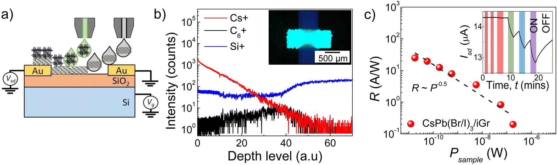 | ||
| Fig. 4 (a) Schematic of inkjet deposition of perovskite NCs on top of iGr to fabricate fully printed detector. (b) Depth profiling of CsPbBr3/iGr heterostructure with 10 printed layers of CsPbBr3 and 10 printed layers of iGr on Si/SiO2 substrate via ToF-SIMS. Inset: optical image of CsPbBr3/iGr heterostructure on Si/SiO2 with 10 layers of CsPbBr3 and 3 layers of iGr under illumination (λex = 365 nm). (c) Photoresponsivity, R, versus power for fully printed CsPb(Br/I)3/iGr heterostructure (1 layer CsPb(Br/I)3 and 1 layer iGr) device with printed AuNP electrodes (1 printed layer) (λex = 520 nm illumination, Vsd = 100 mV, Vg = 0 V). Inset: temporal response of CsPb(Br/I)3/iGr heterostructure device under light illumination (Vsd = 100 mV, Vg = 0 V, P = 56.6 W m−2) at different wavelengths: 1060 nm, 808 nm, 635 nm, 520 nm, 450 nm, and 405 nm, respectively. | ||
The different responsivities measured in perovskite decorated CVD graphene and iGr devices can be attributed to a large (over 3 orders of magnitude) decrease of carrier mobility, which results in longer transport times in iGr, as expected for graphene networks.4 The difference in the responsivity of the iGr-CsPbBr3 hybrid device and the inkjet-printed CsPbBr3/iGr heterostructure devices could be due to the difference in measured sheet resistance. The fully printed CsPb(Br/I)3/iGr device uses an iGr line (R ∼ 5 kΩ) whereas the drop-cast CsPb(Br/I)3/iGr device used a single printed drop of iGr, which has lower number of graphene flakes and higher resistance (R ∼ 10 kΩ). However, the complete interrogation of these differences requires further detailed studies. We suggest that incorporation of perovskite NCs into the matrix of iGr significantly affects electronic transport due to increasing intra-flake distance and porosity. Thus, the nature of the junctions has a significant impact on inter-nanosheet charge transfer, which affects both the carrier mobility and conductivity.32 As such, the change in morphology and porosity of graphene films within the device can lead to large changes in the total conductivity.4 For a percolating network, the total conductance can be described by G = GC/r where r is a characteristic scale of the system and GC is the critical conductance, defined as the junction of lowest conductance within the path of highest total conductance across the full length of the network.34–36 The conductivity between flakes, G, depends exponentially on the flake separation distance, d, G ∼ e−αd where α is the inverse localisation radius, given by α = (2/ħ)√(2mϕ0) where m is the effective mass in the tunnelling region between flakes, and ϕ0 is the work function associated with the flakes.37 Estimating these parameters as the free electron mass, m = 9.11 × 10⁻³¹ kg, and graphene work function, ϕ0 ≈ 4.5 eV,38 we can characterise the difference in measured resistance between the iGr and the iGr-CsPbX3 composite as a small change in the critical distance between percolating flakes, δd ∼ 0.2 nm, caused by the introduction of perovskite NCs into the flake network.
The photoresponsivity achieved in this work is significantly higher than that reported previously,6–10,16 which we attribute to the enhanced stability of all inorganic perovskites used in our work and the optimised ink formulation. Perovskite NCs can be susceptible to environmental degradation, which is normally attributed to the loss of capping ligands and /or poor passivation of surface defects. The presence of a large density of surface defects/traps affects the device performance.39,40 However, our devices maintain stable performance up to two weeks, with only small decrease of photoresponsivity observed following storage in ambient conditions (ESI, SI3 and Fig. S6†). We attribute the higher responsivity observed in our devices to NC stability, which is enabled by efficient surface passivation (and low surface defect density). An additional significant benefit of the enhanced stability of our perovskite NCs is their ability to withstand the inkjet deposition and post deposition processes and provide stable performance in the device.
We demonstrate successful inkjet printing of continuous thin films of all-inorganic perovskite NCs over large areas (>1 cm) and fully printed photodetectors sensitive in the UV-Vis range. The photoresponsivity of >103 A W−1 was demonstrated for both red and green emitting perovskite NC inks on SLG. The lower responsivity R > 101 A W−1 measured for the same perovskite inks used to decorate iGr is explained by lower charge mobility in graphene networks compared to SLG. Our experiments and analysis of the device performance provide a future strategy for development of nanomaterials for fully additively manufactured optoelectronics.
Experimental methods
Substrates and materials
Prime grade silicon wafers with a 200 nm SiO2 thickness were purchased from PI-KEM. Before printing, the substrates were cleaned by sonicating in acetone for 30 minutes at room temperature followed by washing with IPA and drying with N2. Polyimide (Kapton® HN general purpose polyimide film) thermally insulating films were purchased from DUPONT. Before printing, the Kapton was washed with acetone and IPA and dried with N2. High quality CVD grown SLG on Si/SiO2 (300 nm SiO2) field effect transistors (FET) were provided by the Center for nanotechnology innovation at NEST, Italy.41Synthesis of CsPbBr3 NCs
Cs-oleate precursor is made by adding 1.2 mmol of Cs2CO3 together with 18 ml of ODE and 2 ml of OA to a three-necked flask and degassed at 120 °C for 30 min. Then the temperature was increased to 150 °C for 10 min, and a clear and transparent Cs-oleate solution was formed. CsPbBr3 QDs are synthesized using a modified hot-injection method.42 1 mmol of PbO, 3 mmol of phenacyl bromide were mixed with 5 ml of OA and 25 ml of ODE in a 100 ml three-neck flask and degassed under nitrogen for 30 min at 120 °C. The temperature was then increased to 220 °C and 2.5 ml of OA was injected. The solution was annealed for about 20 min. After that, the temperature was lowered to 195 °C and 2.5 ml of Cs-oleate was injected. The solution was kept for 5 min at temperature of 195 °C and cooled to room temperature by an ice water bath. To obtain the final product, the compound powder was purified by washing twice with isopropanol and dried under vacuum. The red CsPb(Br/I)3 QDs were prepared through ion exchange method, with the PbI2-OA as an I-ion precursor.Ink formulations
The ink used to deposit inkjet-printed graphene (iGr) was purchased from Sigma-Aldrich (product number: 793663). The ink contains liquid exfoliated graphene flakes with an average size of 2590 nm2 and ethyl cellulose (EC) with a 2.4 wt% solids concentration; dispersed in an 85:15 mixture of cyclohexanone/terpineol to provide a suitable rheology for jetting. The ink had a density of 9.665 g cm−3, surface tension of 33 mN m−1, and viscosity of 11.3 mPa·s at room temperature.
The hybrid ink containing iGr and CsPbX3 NCs (iGr-CsPbX3) was formulated by dispersing 5 mg ml−1 of CsPbX3 NCs in a mixture of the commercial iGr ink and hexane (2:1 v/v) and sonicating for 30 minutes at room temperature. The hybrid ink had viscosity of 2.96 mPa·s, surface tension of 27.4 mN m−1, and density of 0.93 g ml−1. CsPbX3 NC inks were formulated for inkjet printing by dispersing 5 mg ml−1 CsPbX3 NCs in a mixture of hexane, cyclohexanone, and terpineol (1:3:1 v/v) and sonicating for 30 minutes at room temperature. All inks were stored in Fujifilm Dimatix cartridges at room temperature. Graphene ink cartridges were stored in ambient conditions, and perovskite-based ink cartridges were stored under a N2 atmosphere.
Inkjet printing process
Films were printed on Si/SiO2 and on flexible Kapton substrates using a drop-on-demand (DoD) piezo-driven Fujifilm Dimatix DMP-2800 inkjet printer. In each print, a single nozzle was used to deposit single lines in the x-direction sequentially. To print additional layers, this process was repeated directly on top of the previous layer. The morphology of printed films is dictated by the drop spacing, which is the distance between the centres of neighbouring drops deposited by the printer. The printing parameters optimised for iGr4 were also used for the iGr-CsPbX3 hybrid ink deposition, using a 10 pl drop volume cartridge (DMC-11610) with nozzles of diameter of 21.5 μm, which formed spots with a diameter of ∼50 μm on Si/SiO2. The hybrid ink was deposited with a drop spacing of 20 μm, the printer was paused for 30 seconds between printing each layer, and nozzles were purged before printing each layer and periodically during printing (for 0.1 s every 100 printed swaths) to achieve consistent jetting. For the perovskite NC inks, printing was performed with Fujifilm Dimatix Samba cartridges with a 2.4 pl drop volume and nozzle diameter 17 μm, which formed printed spots with a diameter of ∼40 μm on Si/SiO2. Perovskite NCs were deposited with a drop-spacing of 20 μm at a substrate temperature of 60 °C in N2 atmosphere. A leader bar (a small redundant bar printed to the left of prints) was used for all prints to ensure favourable jetting at the beginning of each printed swath. Printed films were annealed in a vacuum oven at ∼1 mbar vacuum. The iGr and i(Gr-CsPbBr3) hybrid were annealed at 250 °C for 30 min.The AuNP ink was deposited with a 10 pl drop volume cartridge (DMC-11610) with nozzle temperature of 35 °C, substrate temperature of 90 °C, and a drop spacing of 30 μm, as described by J. Im, et al.33 Films were then sintered at 150 °C for 30 min.
Drop-casting
A single drop of CsPb(Br/I)3 NC solution (4 mg ml−1 in hexane) was drop-cast onto iGr to form a CsPb(Br/I)3/iGr heterostructure device for comparison with inkjet deposited CsPb(Br/I)3.Transmission electron microscopy
Transmission electron microscopy (TEM) images were acquired on a JEM-2100F, JOEL operated at 200 kV and were analysed using ImageJ43 for nanoparticle size measurements.Optical characterisation
Photoluminescence (PL) mapping of CsPbBr3 was performed under vacuum using a 405 nm pulsed delta diode laser as the excitation source (pulse rate of 100 MHz with a time-averaged power ∼10 μW and a spot size of ∼2 μm) and a Horiba MicOS optical spectrometer with Si CCD array detector and 50× objective, NA: 0.5, and 150 mm−1 grating. The samples were moved in steps of 20 μm using a motorised Zaber stage attached to the vacuum chamber/cryostat. The CsPb(Br/I)3 PL spectrum was obtained using a frequency-doubled Nd:YVO4 laser (wavelength λ = 532 nm, power, P = 70 μW, and a spot size of ∼5 μm) for optical excitation. The laser was used in continuous wave (CW) mode and PL spectra were recorded using a Horiba LabRAM system equipped with a Si CCD array detector.Optical absorbance measurements were conducted with a Cary 3500 UV-Vis spectrophotometer using a 1 mg ml−1 solution of the CsPb(Br/I)3 ink and 0.5 mg ml−1 solution of the CsPbBr3 ink in polystyrene cuvettes.
Electrical measurements
Electrical measurements and photocurrent measurements were performed using Keithley-2400 Source-Meters and Keitheley-2010 multimeters in DC mode. Carrier mobility in graphene was calculated from σsd(Vg) dependences using the equation μ = σsd/Vg × d/ε0ε where d = 300 nm and ε = 3.9 correspond to the thickness and dielectric constant of the used SiO2 layer, respectively.30Fixed wavelength excitations were provided by a set of six fibre-coupled diode-pumped solid state DPSS lasers with calibrated output power ≤30 mW for all output wavelengths (λex = 405, 450, 532, 635, 808, 1060 nm). A MicroHR monochromator (Horiba, MHRA-2X-FS, with 75 W xenon source) was used for photocurrent measurements under tuneable wavelength (λ = 200 nm to 1000 nm). Photoresponsivity (R) was calculated by R = Ipc/Psample where Ipc is the maximum change in source–drain current (Isd) recorded after one minute of constant illumination and Psample is the total light power incident on the sample. Electrical studies under mechanical deformation were performed using mechanical bending setup equipped with a stepper motor. The speed, length, and the number of bending cycles was controlled using the DRV8825 stepper driver. A bending radius of 0.5 cm was used and during bending cycles, Isd was measured continuously, and I(V) characteristics were measured at intervals between bending cycles.
Depth profiling
Chemical depth profiling was done using time-of-flight secondary ion mass spectrometry (ToF-SIMS). ToF-SIMS 3D mapping was carried out using a TOF.SIMS 5 instrument from IONTOF GmbH in a dual-beam fashion. The ToF-SIMS data were acquired in positive ion polarity mode by raster scanning a 30 keV Bi3+ primary ion beam and delivering 0.08 pA. The sputter beam was an argon gas cluster ion beam (GCIB) operated with energies between 5 and 7.5 keV and 1500 atoms in the cluster with up to 4 nA beam current. A low-energy (20 eV) electron flood gun was employed to neutralise charge build up. Prior to profiling a heterostructure, profiles of pure inkjet-printed perovskite NCs and pristine inkjet-printed graphene were acquired to establish characteristic signal for each material.Conclusions
In this work we formulated all-inorganic lead halide perovskite nanocrystals for inkjet deposition. The stability of the perovskites used and of the ink developed, enabled us to explore the potential of these inks as photosensitive layers in graphene based photon detectors, including fully printed devices. Our work addresses current challenges by increasing the availability of optically active materials for additive manufacturing technologies. Establishing a library of conductive (AuNP and graphene inks) and semiconducting (perovskite nanocrystals) materials, we achieved printed photon detectors with the highest photoresponsivity in UV-vis range reported to date for similar inkjet fabricated devices. We also demonstrated perovskite/graphene devices produced using a combination of different techniques, from conventional device processing to inkjet printing. Performance of the fabricated devices was explained using the photoresponsivity model based on the ratio of photoexcited charge trapping/electron transport time or responsivity/response time ratio. The results reported here are of fundamental and technological interest, as it provides opportunities for surface functionalisation of devices produced using convectional Si-technologies as well as potential applications in flexible/wearable optoelectronics.Author contributions
J. A. and F. W. formulated inks and performed inkjet printing, C. Z. synthesised perovskites, J. A. and N. C. performed electrical measurements, T. J., P. B., O. N. D. and C. Z. performed optical measurements; JG performed charge transport modelling, G. T. and Y. Z. performed ToF-SIMS. C. T., R. H., O. M. and L. T. conceptualised the studies. All authors analysed the results, co-wrote the manuscript and approved its submission.Conflicts of interest
Authors declare no conflict of interest.Acknowledgements
This work was funded by the Engineering and Physical Sciences Research Council award “Enabling Next Generation Additive Manufacturing” [grant number EP/P031684/1]. The authors acknowledge access to facilities at the Nanoscale and Microscale Research Centre (nmRC) of the University of Nottingham and School of Pharmacy; C. Coletti and V. Miseikis (Center for Nanotechnology Innovation @NEST, Istituto Italiano di Tecnologia, Pisa, Italy) for providing CVD graphene devices; Dr J. Im for providing gold nanoparticle ink and Dr M. Fay for TEM studies.References
- C. H. Liu, Y. C. Chang, T. B. Norris and Z. Zhong, Nat. Nanotechnol., 2014, 9, 273–278 CrossRef CAS PubMed.
- N. D. Cottam, C. Zhang, L. Turyanska, L. Eaves, Z. Kudrynskyi, E. E. Vdovin, A. Patanè and O. Makarovsky, ACS Appl. Electron. Mater., 2020, 2, 147–154 CrossRef CAS.
- Z. Li, K. Xu and F. Wei, Nanotechnol. Rev., 2018, 7, 393–411 CrossRef CAS.
- F. Wang, J. H. Gosling, G. F. Trindade, G. A. Rance, O. Makarovsky, N. D. Cottam, Z. Kudrynskyi, A. G. Balanov, M. T. Greenaway, R. D. Wildman, R. Hague, C. Tuck, T. M. Fromhold and L. Turyanska, Adv. Funct. Mater., 2021, 31, 2007478 CrossRef CAS.
- K. Cho, T. Lee and S. Chung, Nanoscale Horiz., 2022, 7, 1161–1176 RSC.
- Z. Gu, Y. Wang, S. Wang, T. Zhang, R. Zhao, X. Hu, Z. Huang, M. Su, Q. Xu, L. Li, Y. Zhang and Y. Song, Nano Res., 2022, 15, 1547–1553 CrossRef CAS.
- Q. Wang, G. Zhang, H. Zhang, Y. Duan, Z. Yin and Y. Huang, Adv. Funct. Mater., 2021, 31, 2100857 CrossRef CAS.
- V. R. F. Schröder, F. Hermerschmidt, S. Helper, C. Rehermann, G. Ligorio, H. Näsström, E. L. Unger and E. J. W. List-Kratochvil, Adv. Eng. Mater., 2021, 24, 2101111 CrossRef.
- Y. Liu, F. Li, C. Perumal Veeramalai, W. Chen, T. Guo, C. Wu and T. W. Kim, Appl. Mater. Interfaces, 2017, 9, 11662–11668 CrossRef CAS PubMed.
- M. Min, R. F. Hossain, N. Adhikari and A. B. Kaul, ACS Appl. Mater. Interfaces, 2020, 12, 10809–10819 CrossRef CAS PubMed.
- H. Lee, W. Harden-Chaters, S. D. Han, S. Zhan, B. Li, S. Y. Bang, H. W. Choi, S. Lee, B. Hou, L. G. Occhipinti and J. M. Kim, ACS Appl. Nano Mater., 2020, 3, 4454–4464 CrossRef CAS.
- M. J. Grotevent, C. U. Hail, S. Yakunin, D. Bachmann, M. Calame, D. Poulikakos, M. V. Kovalenko and I. Shorubalko, Adv. Sci., 2021, 8, 2003360 CrossRef CAS PubMed.
- M. J. Grotevent, C. U. Hail, S Yakunin, D. N. Dirin, K. Thodkar, G. Borin Barin, P. Guyot-Sionnest, M. Calame, D. Poulikakos, M. V. Kovalenko and I. Shorubalko, Adv. Opt. Mater., 2019, 7, 1900019 CrossRef.
- G. Pace, A. Grimoldi, D. Natali, M. Sampietro, J. E. Coughlin, G. C. Bazan and M. Caironi, Adv. Mater., 2014, 26, 6773–6777 CrossRef CAS PubMed.
- Z. Tao, H. Lin, Y. Zhu, D. Hu, W. Yang, J. Pan and X. Liu, IEEE Photonics J., 2022, 14, 6802605 CAS.
- A. M. Alamri, S. Leung, M. Vaseem, A. Shamim and J. H. He, IEEE Trans. Electron Devices, 2019, 66, 2657–2661 CAS.
- S. Saggar, S. Sanderson, D. Gedefaw, X. Pan, B. Philippa, M. R. Andersson, S. C. Lo and E. B. Namdas, Adv. Funct. Mater., 2021, 31, 2010661 CrossRef CAS.
- J. Liu, M. Gao, J. Kim, Z. Zhou, D. S. Chung, H. Yin and L. Ye, Mater. Today, 2021, 51, 475–503 CrossRef CAS.
- G. Hu, T. Albrow-Owen, X. Jin, A. Ali, Y. Hu, R. C. T. Howe, K. Shehzad, Z. Yang, X. Zhu, R. I. Woodward, T. C. Wu, H. Jussila, J.-B. Wu, P. Peng, P. H. Tan, Z. Sun, E. J. R. Kelleher, M. Zhang, Y. Xu and T. Hasan, Nat. Commun., 2017, 8, 278 CrossRef PubMed.
- F. Mathies, E. J. W. List-Kratochvil and E. L. Unger, Energy Technol., 2020, 8, 1900991 CrossRef CAS.
- R. Sliz, M. Lejay, J. Z. Fan, M. J. Choi, S. Kinge, S. Hoogland, T. Fabritius, F. P. Garciá De Arquer and E. H. Sargent, ACS Nano, 2019, 13, 11988–11995 CrossRef CAS PubMed.
- C. Zhang, L. Turyanska, H. Cao, L. Zhao, M. W. Fay, R. Temperton, J. O′shea, N. R. Thomas, K. Wang, W. Luan and A. Patanè, Nanoscale, 2019, 11, 13450–13457 RSC.
- J. Liu, B. Shabbir, C. Wang, T. Wan, Q. Ou, P. Yu, A. Tadich, X. Jiao, D. Chu, D. Qi, D. Li, R. Kan, Y. Huang, Y. Dong, J. Jasieniak, Y. Zhang and Q. Bao, Adv. Mater., 2019, 31, 1901644 CrossRef PubMed.
- C. Kang, Z. Zhou, J. E. Halpert and A. K. Srivastava, Nanoscale, 2022, 14, 8060–8068 RSC.
- S. Bera, R. K. Behera and N. Pradhan, J. Am. Chem. Soc., 2020, 142, 20865–20874 CrossRef CAS PubMed.
- Y. Su, Q. Zeng, X. Chen, W. Ye, L. She, X. Gao, Z. Ren and X. Li, J. Mater. Chem. C, 2019, 7, 7548–7553 RSC.
- X. Yu, R. Xing, Z. Peng, Y. Lin, Z. Du, J. Ding, L. Wang and Y. Han, Chin. Chem. Lett., 2019, 30, 135–138 CrossRef CAS.
- A. Gao, J. Yan, Z. Wang, P. Liu, D. Wu, X. Tang, F. Fang, S. Ding, X. Li, J. Sun, M. Cao, L. Wang, L. Li, K. Wang and X. W. Sun, Nanoscale, 2020, 12, 2569–2577 RSC.
- N. D. Cottam, J. S. Austin, C. Zhang, A. Patanè, W. Escoffier, M. Goiran, M. Pierre, C. Coletti, V. Mišeikis, L. Turyanska and O. Makarovsky, Adv. Electron. Mater., 2022, 2200995 CrossRef.
- S. V. Morozov, K. S. Novoselov, M. I. Katsnelson, F. Schedin, D. C. Elias, J. A. Jaszczak and A. K. Geim, Phys. Rev. Lett., 2008, 100, 016602 CrossRef CAS PubMed.
- L. Turyanska, O. Makarovsky, S. A. Svatek, P. H. Beton, C. J. Mellor, A. Patanè, L. Eaves, N. R. Thomas, M. W. Fay, A. J. Marsden and N. R. Wilson, Adv. Electron. Mater., 2015, 1, 1500062 CrossRef.
- S. Barwich, J. Medeiros de Araújo, A. Rafferty, C. Gomes da Rocha, M. S. Ferreira and J. N. Coleman, Carbon, 2021, 171, 306–319 CrossRef CAS.
- J. Im, G. F. Trindade, T. T. Quach, A. Sohaib, F. Wang, J. Austin, L. Turyanska, C. J. Roberts, R. Wildman, R. Hague and C. Tuck, ACS Appl. Nano Mater., 2022, 5, 6708–6716 CrossRef CAS PubMed.
- N. Tessler, Y. Preezant, N. Rappaport and Y. Roichman, Adv. Mater., 2009, 21, 2741–2761 CrossRef CAS.
- M. C. J. M. Vissenberg and M. Matters, Phys. Rev. B: Condens. Matter Mater. Phys., 1998, 57, 12964 CrossRef CAS.
- V. Ambegaokar, B. I. Halperin and J. S. Langer, Phys. Rev. B: Solid State, 1971, 4, 2612 CrossRef.
- J. G. Simmons, J. Appl. Phys., 1963, 34, 1793 CrossRef.
- S. M. Song, J. K. Park, O. J. Sul and B. J. Cho, Nano Lett., 2021, 12, 3887–3892 CrossRef PubMed.
- L. Kong, Y. Luo, L. Turyanska, T. Zhang, Z. Zhang, G. Xing, Y. Yang and C. Zhang, Adv. Funct. Mater., 2022, 2209186 Search PubMed.
- D. A. Kara, D. Cirak and B. Gultekin, Phys. Chem. Chem. Phys., 2022, 24, 10384–10393 RSC.
- S. Pezzini, V. Mišeikis, S. Pace, F. Rossella, K. Watanabe, T. Taniguchi and C. Coletti, 2D Mater., 2020, 7, 041003 CrossRef CAS.
- J. N. Yang, T. Chen, J. Ge, J. J. Wang, Y. C. Yin, Y. F. Lan, X. C. Ru, Z. Y. Ma, Q. Zhang and H.-B. Yao, J. Am. Chem. Soc., 2021, 143, 19928–19937 CrossRef CAS PubMed.
- ImageJ, https://imagej.nih.gov/ij/index.html, (accessed 29 June 2022).
Footnotes |
| † Electronic supplementary information (ESI) available. See DOI: https://doi.org/10.1039/d2nr06429d |
| ‡ Authors equally contributed to the work. |
| This journal is © The Royal Society of Chemistry 2023 |