
 Open Access Article
 This Open Access Article is licensed under a
 Creative Commons Attribution 3.0 Unported Licence
Single-particle optical study on the effect of chloride post-treatment of MAPbI3 nano/microcrystals†
Handong
Jin‡
a,
Amitrajit
Mukherjee‡
a,
Lata
Chouhan
a,
Julian A.
Steele
 bd,
Flip
de Jong
a,
Yujie
Gao
b,
Maarten B. J.
Roeffaers
b,
Johan
Hofkens
*ac and
Elke
Debroye
*a
bd,
Flip
de Jong
a,
Yujie
Gao
b,
Maarten B. J.
Roeffaers
b,
Johan
Hofkens
*ac and
Elke
Debroye
*a
aDepartment of Chemistry, KU Leuven, Celestijnenlaan 200F, Leuven, Belgium. E-mail: johan.hofkens@kuleuven.be; elke.debroye@kuleuven.be
bcMACS, Department of Microbial and Molecular Systems, KU Leuven, 3001 Leuven, Belgium
cMax Planck Institute for Polymer Research, Ackermannweg 10, 55128 Mainz, Germany
dSchool of Mathematics and Physics, The University of Queensland, Brisbane, QLD 4072, Australia
First published on 22nd February 2023
Abstract
Surface passivation by post-treatment with methylammonium chloride (MACl) is regarded as a promising strategy to suppress surface defects in organic–inorganic lead halide perovskites and elevate the efficiency of solar cells based on these materials. However, traditional MACl post-treatment methods often impede the performance of the final device, due to the creation of additional unwanted defects. Herein, we report a novel approach for chloride post-treatment by applying a mixed ethanol/toluene solvent and validate its beneficial effect on the structure, composition, and optical properties of methylammonium lead iodide nano/microcrystals and related photosensitive devices. An optimized (mild) Cl content improves the crystallinity, enhances photoluminescence (PL) intensity, provides longer PL lifetimes, and induces brighter and longer ON-states in single-particle emission trajectories. On top of a reduction in the population percentage of crystals showing gradual photodegradation, our Cl-treatment method even leads to photobrightening. Additionally, the extent of carrier communication throughout spatially distant nanodomains enhances after MACl-based post-modification. Our results demonstrate that surface-bound Cl significantly reduces the trap density induced by under-coordinated lead ions or iodide vacancies and reveal the importance of a careful consideration of the applied Cl content to avoid the generation of high-bandgap MAPbCl3 heterojunctions upon excessive Cl treatment. Importantly, significant trap passivation upon MACl treatment translates into a more stable and elevated photocurrent in the corresponding photodetector device. We anticipate these findings will be beneficial for designing durable, high-performance lead halide perovskite photonic devices.
Introduction
Organic–inorganic metal lead halide perovskites (MHPs) with an APbX3 chemical formula (where A is an organic cation such as methylammonium (MA) or formamidinium (FA), and X is Cl, Br or I) are currently considered promising materials for photovoltaic (PV) devices due to the high power conversion efficiency (PCE)1 obtained by low-cost solution processing.2 So far, the PCE has been benchmarked at 25.7% for single-junction devices,1 approaching the theoretical limit of 31%.3 However, poor long-term stability and PCE efficiency are still two major hurdles4 preventing the commercialization of perovskite solar cells. In particular, harmful defects with formation energies residing in the bandgap, such as interstitial and anti-site defects, cannot be avoided in solution-processed perovskite thin films. These deep traps inherently result in efficiency losses by the non-radiative (NR) recombination of photogenerated charge carriers.5,6Compared to its Br and Cl-counterparts, MAPbI3 is the most studied MHP material for application in perovskite solar cells. The extrinsic defects existing on the crystal surface, such as under-coordinated lead/iodide ions5 and lead-iodide anti-sites,7 usually create deep traps inside the bandgap and often result in significant efficiency losses. These surface defect sites also play an important role in the layer-by-layer degradation of the perovskite.8–10 Several work has been done previously to prevent such defects11 and passivate the perovskite surface to improve its optical and electronic properties and stability.12–14 While chloride doping is being adopted,15,16 chloride post-treatment has also been shown to raise the PL intensity and elongate the PL lifetimes,13,17 which likely indicates passivation of the surface defects. However, a decreased PV efficiency13,18 or rapid perovskite degradation17,19 could not be avoided. The responsible factors are the usage of a polar solvent (methanol, ethanol, or isopropanol) which dissolves the perovskite, and the integration of excessively added small chloride ions inside the iodide-based perovskite which forms higher-bandgap MAPbCl3 heterojunctions.13,18 In other words, the commonly used post-treatment method induces the passivation of surface defects but also leads to the formation of new ones.20 For example, additional deep traps (∼0.52 eV) appear after partially suppressing the trap density (∼0.67 eV) in MACl post-treated MAPbI3 thin films.13 Therefore, developing a new post-treatment strategy to sustain the perovskite quality along with qualitative investigation of trap-involved photophysics in single MHP crystals before and after the Cl-based surface passivation are in demand.
Furthermore, the commonly probed PL enhancement and extended PL lifetimes as indicators of reduction in trap density may hitherto been reliable but not be very conclusive as longer lifetime may be assigned to less grain boundaries even having higher density of traps.13 A more direct technique to reliably assess the density of traps can be investigation of the PL blinking using single particle fluorescence microscopy. Comparison and analysis of the blinking characteristic before and after the post-treatment can potentially untangle the differences in trap density as well as photophysics of nano-/microcrystals (NCs/MCs).21–23 This is certainly impossible to probe using conventional bulk steady-state and time-resolved PL spectroscopic measurements. Especially, as polycrystalline MHP thin films usually exhibit a relatively high number of defects, monocrystalline NCs/MCs of low trap density5 can attract more attention in photovoltaics.24–26,54 This further enables independent scope to study the influence of traps on optical and electronic properties in absence of grain boundaries. Hence, we explicitly focus on the variation in trap density and the optical behavior of (un)treated MAPbI3 crystals within the bulk solution and at single-particle level.
Here, we report a novel method involving MACl post-treatment in a mixed (ethanol/toluene) solvent for passivating the surface of MAPbI3 crystals (Fig. S1†). We selectively choose MACl based passivation as smaller sized chloride ions can easily approach the surface defects, form stronger Pb–Cl bonds, and reduce the lattice strain upon decreasing the Pb–X bond length.17 Besides, photo-induced ion migration and new defect generation, even after the post treatment,15 which is very common in case of iodine-based systems, can be avoided by formation of the strong Pb–Cl bond. In particular, we added minute concentrations of MACl in ethanol to the toluene suspension of MAPbI3 crystals. The usage of a limited volume of ethanol effectively dissolves the MACl salt while simultaneously, it is less harmful toward perovskite degradation during the post-treatment process. Structural and optical characteristics of the synthesized samples have been systematically explored. X-ray photoelectron spectroscopy (XPS) and energy-dispersive X-ray spectroscopy (EDS) reveal the existence of chloride on the surface of MAPbI3 crystals. The bulk PL spectroscopy shows higher PL quantum yields (PLQYs) along with enhanced PL lifetimes for the Cl-treated crystals. Further, suppression of PL blinking in post-treated crystals directly evidences the reduction of defects by surface-coordinated chloride ions. On top of the decrease in population percentage of crystals showing gradual photodegradation, our Cl-treatment approach even leads to temporal photobrightening. Finally, the significant photocurrent enhancement of a mild Cl-treated MAPbI3-based photodetector device confirms the suppressed trap density, illustrating feasible translation of this approach into manufacturing of efficient optoelectronic devices.
Results and discussion
To pinpoint the critical limit of surface passivation, and thereby avoid excessive Cl treatment, we deliberately investigated MAPbI3 crystals with low (3%), moderate (9%) and high (17%) percentages of MACl post-treatment. The size distribution and morphology of pristine, as well as 3%, 9% and 17%Cl post-treated MAPbI3 NCs/MCs are evaluated by SEM imaging (Fig. 1a and Fig. S2†). The MAPbI3 NCs (<1 μm) are considered before and after the post-treatment which comprises an average dimension of 500 nm (Fig. 1b). The mean size of the investigated (un)treated MCs is 1.58 μm (Fig. S3†). While alcohols like ethanol13 and isopropanol18,27 are commonly used for the post-treatment of the perovskite surface, they parallelly result in partial decomposition by forming binary halide components (MAI and PbI2).13 However, the use of nonpolar toluene with a relatively small volume of ethanol is expected to be benign and minimize potential damage to the perovskite. As seen in Fig. S2,† no visible size and morphology changes are observed for the NCs/MCs before and after chloride post-treatment which indicates no large-scale destructive effect of the mixed-solvent approach on the particles. XRD is conducted to understand the impact on the crystal structure induced by MACl post-treatment. Fig. 1c shows the diffractograms obtained from pristine along with 3%, 9% and 17%Cl treated MAPbI3 crystals. The pristine MAPbI3 crystals showed peaks at 13.9° and 14.1°, corresponding to the tetragonal perovskite phase. For MAPbI3-3%Cl, the same peak shape and positions are observed, indicating Cl− adsorption on the surface does not change the MAPbI3 crystalline structure even after the post-treatment. Upon higher chloride content (9%Cl), a new small peak appears at 15.6° (Fig. S4b† and Fig. 1c) which originates from the formation of MAPbCl3 (Fig. S5†) on the crystal surface.28 This peak is enhanced with 17%Cl post-treatment (Fig. S4b†). The appearance of the MAPbCl3 phase is expected to be the result of ion exchange of iodide by chloride on the particle surface. However, no other alteration in the peak positions or morphology (as shown in Fig. S4a†) can be observed. Our results reveal unavoidable formation of MAPbCl3 in intensively Cl-treated MAPbI3 crystals (9% and 17%Cl treatment), which however only affects the crystal surface rendering no change in the bulk MAPbI3 crystal structure.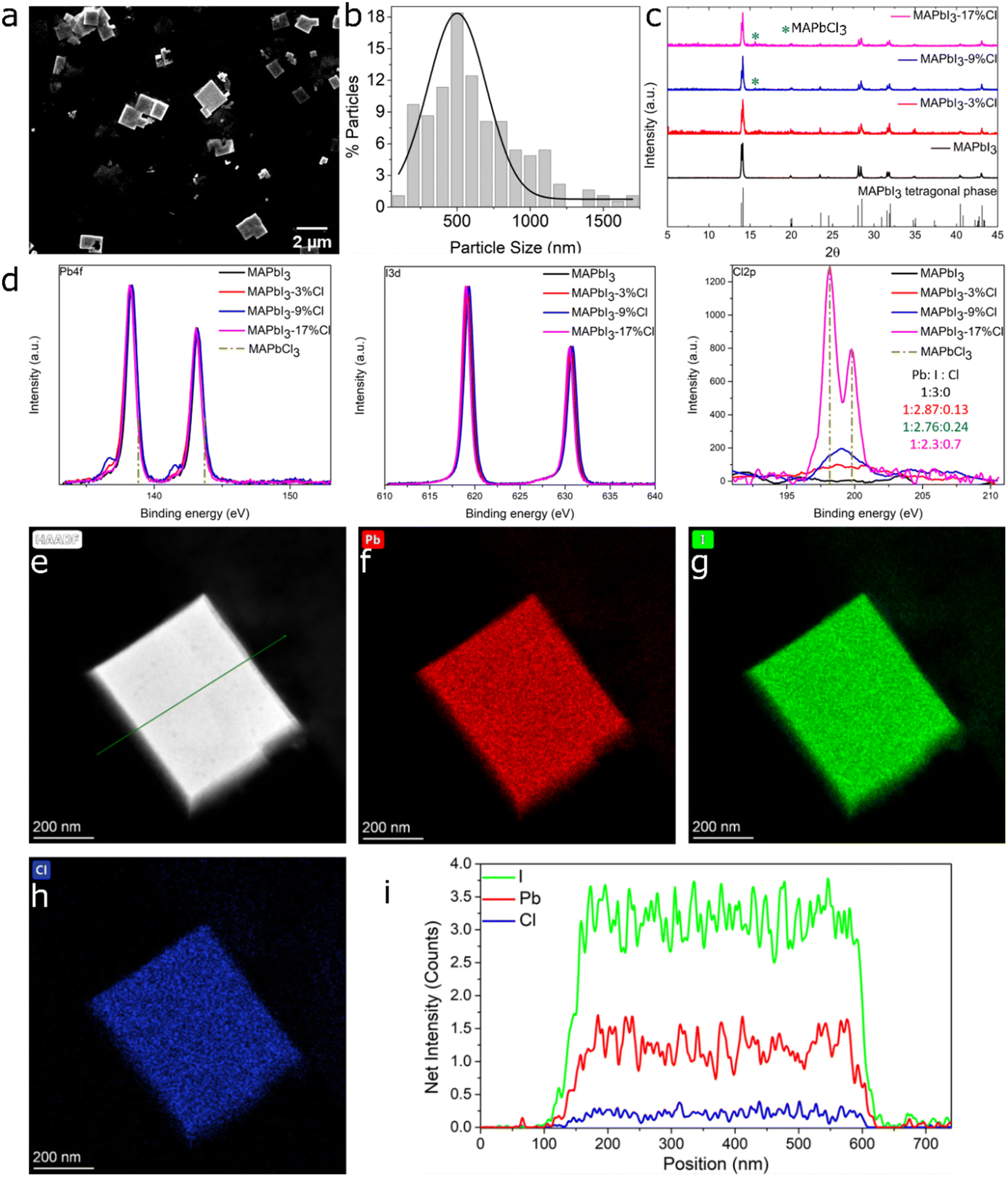 | ||
| Fig. 1 SEM image (a) and size distribution histogram (b) of the edge lengths of the MAPbI3 NCs. XRD patterns of MAPbI3 crystals (c) with 0, 3, 9, and 17%Cl post-treatment. XPS spectra (d) of Pb 4f, I 3d and Cl 2p core levels for MAPbI3 crystals without and with chloride post-treatment and for MAPbCl3. Pb 4f and Cl 2p energy-level positions of MAPbCl3 are indicated by dashed lines.29 HAADF-STEM image (e) and STEM-EDS elemental mapping (f–h) of Pb, I, and Cl of a 17%Cl post-treated MAPbI3 NC. A STEM-EDS line scan (i) of the same NC. | ||
The XPS study unravels the surface elemental composition after chloride treatment (Fig. 1d and Fig. S6†). Two main peaks consisting of Pb 4f5/2 (141–146 eV) and Pb 4f7/2 (136–140 eV) belong to the spin–orbit splitting of the f-orbital, suggesting Pb is in +2 oxidation state. The small peaks appearing at 136.8 eV and 141.5 eV point to the presence of Pb0. These features are often reported and assigned to beam-induced damage.29–31 In principle, a right shift (<0.5 eV for MAPbI3-3%Cl crystals; 0.5 eV for MAPbI3-9%Cl and MAPbI3-17%Cl crystals) of the two splitted Pb 4f peaks would appear in case of surface adsorbed Cl− and MAPbCl3 formation due to the different nature of lead-halide bonding. Those two shifted Pb2+ peaks are possibly covered by the strong signal of MAPbI3. The masking of the Cl-signal by MAPbI3 is confirmed by the spectrum of Cl 2p in Fig. 1d. The Cl 2p spectrum of the 3%, 9% and 17%Cl post-treated MAPbI3 crystals consists of the spin–orbit splitted peaks of Cl 2p3/2 and Cl 2p1/2 at binding energy values of 198.15 eV and 199.79 eV, suggesting the formation of a Cl–Pb covalent bond.29 The masking of Cl-signal suggests that adsorption of Cl− moiety (or formation of MAPbCl3) is strictly present on the surface and not penetrate through the bulk of mildly/intensively Cl-treated MAPbI3 crystals. This is further verified for 17%Cl-treated MAPbI3 crystals, in which formation of a shallow layer of MAPbCl3 is confirmed from the EDS spectra (Fig. S7 and S8†). Distribution of carbon, nitrogen, lead, iodide and chloride in the representative MAPbI3-17%Cl NC can be found in the STEM-EDS elemental mapping (Fig. 1e–h). However, the ratio of Pb to I remains almost equal to 1![[thin space (1/6-em)]](https://www.rsc.org/images/entities/char_2009.gif) :3 as per the XPS and STEM-EDS measurement (Fig. 1d and i). The HAADF-STEM image and STEM-EDS elemental mapping of the representative MAPbI3-3%Cl and MAPbI3-9%Cl are depicted in Fig. S9 and S10.†
:3 as per the XPS and STEM-EDS measurement (Fig. 1d and i). The HAADF-STEM image and STEM-EDS elemental mapping of the representative MAPbI3-3%Cl and MAPbI3-9%Cl are depicted in Fig. S9 and S10.†
Fig. 2a depicts the UV-vis absorption and steady-state bulk (in toluene) PL of the MAPbI3 crystals with 0, 3, 9, and 17%Cl post-treatment. The similar bandgap (∼1.56 eV, Fig. S11†) and PL maximum (λ = 779–784 nm) for pristine and Cl-treated MAPbI3 crystals as shown in Fig. 2a, are also in agreement that adsorbed Cl− or MAPbCl3 is only present on the crystal surface. The gradual blue-shift and enhanced PL intensities could suggest (i) a relatively larger bandgap due to the band offset between two semiconductor materials in case of formation of MAPbCl3 on the crystal surface32,33 (see additional discussion in the ESI†) or (ii) suppressed tail states due to a decrease of trap densities after surface passivation.34 Since a thin MAPbCl3 layer is only observed at the surface of intensively Cl-treated (9% and 17%Cl) MAPbI3 crystals (see previous section), our observation implies that trap density suppression is significant for mildly Cl-treated (3%Cl) MAPbI3 crystals.
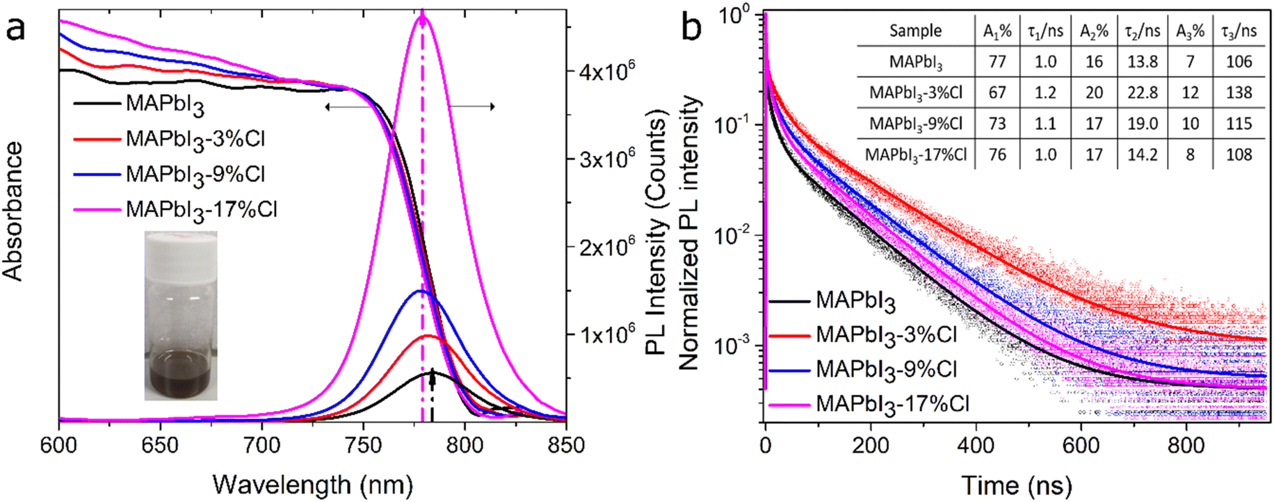 | ||
| Fig. 2 PL and UV-Vis absorption spectra (a) of MAPbI3 crystals upon 0, 3, 9 and 17%Cl post-treatment. Normalized time-resolved PL decay (b) and fitted curves of MAPbI3 crystals with the addition of 0, 3, 9, and 17%Cl (ensemble measurement on a drop of the crystal suspension on a cover glass; fitted parameters for a multiexponential fit (the reduced χ2 Chi-square value is 1 < χ2 < 2.9) are given in the inset table with ‘A’ amplitude and ‘τ’ lifetime), measured in air with pulsed excitation (485 nm, 1 MHz, 1.9 × 10¹⁴ photons per cm3). | ||
Time-resolved PL decay curves of an ensemble of MAPbI3 crystals deposited on glass cover slides are recorded (Fig. 2b) to quantify the charge carrier dynamics. Using a tri-exponential fit (1 < χ2 < 2.9) the fast lifetime component can been related to bound excitons, the intermediate lifetime to exciton recombination, and the longer lifetime component is attributed to free charge carrier dynamics.35 The pristine MAPbI3 crystals show PL lifetime (τ) values of 1.0 (τ1), 13.8 (τ2), and 106 ns (τ3), respectively. Upon 3%Cl post-treatment, higher τ values of 1.2, 22.8, and 138 ns are measured. Furthermore, a higher contribution for τ3 (A3 = 8–12% for passivated vs. 7% for pristine) is observed for the Cl-treated MAPbI3 crystals. A similar long PL lifetime has been reported16,36 for MAI and octylammonium iodide passivated MAPbI3 films. Increased PL lifetime along with higher contribution of the longer lifetime components are attributed to the enhanced number of free charge carriers, indicating a suppressed trap-assisted NR recombination. In our case, mildly-chloride treated (3%Cl) MAPbI3 crystals show highest average PL lifetime (Fig. S12†) along with highest (lowest) contribution from the longest (fast) lifetime component, which indicate suppressed NR recombination of the photogenerated charge carriers.27,37 The average PL lifetime and contribution of longer lifetime components decrease upon the appearance of a tiny amount of MAPbCl3 in MAPbI3-9%Cl and MAPbI3-17%Cl crystals, indicating higher trap densities than MAPbI3-3%Cl crystals (see Note 2, ESI†). Albeit the steady-state measurements show increasing PL intensity upon Cl-treatment, lifetime study unveils that a nominal passivation (3%Cl) is beneficial to efficiently reduce the trap density. It further emphasizes the harmfulness of heavy Cl-treatment (9%, 17%) due to forming a layer of MAPbCl3 on the MAPbI3 crystal surface which likely creates a greater number of NR defect states at the interface. Although the experimental conditions (perovskite films/crystals, applied salts and/or solvents, etc.) are different, we have compared our results with previously observed PL lifetime changes upon halide (X = Cl−, I−) doping or post-treatment of MAPbI3 (-based) materials. A tabular summary (Table S1†) shows an enhanced PL lifetime of MAPbI3 NCs/films using different salt treatment or doping strategies. However, comparison of lifetime components and probing a critical salt concentration to reach the maximum benefit of passivation have not been demonstrated.19 Here, our result seeks importance as it shows the disadvantage of an excessive MACl concentration on the carrier lifetime which is crucial to optimize the post-treatment process.
As demonstrated in one of our previous reports,15 monitoring PL intermittency (blinking) of individual crystals is one of the keys to correctly monitor potential changes of trap densities before and after the chloride post-treatment. We have carefully selected around 50 individual NCs (<1 μm) of each compositions using the integrated wide-field fluorescence microscopy/SEM imaging instrument, which show clear two-state PL blinking. Fig. 3a demonstrates PL intensity transient of a representative non-post-treated MAPbI3 NC distributed within bright (ON) and dim (OFF) states (tON/OFFs). According to established theories, ON and OFF state durations in MHP NCs are related to the rate of switching between passive/active states of the recombination centers associated with NR trap(s).23 Active NR centers are presumably created by ion migration and thereby temporary generation of localized charges which create NR states to acts as carrier traps.23 Generation of the NR centers reduces under stable passive states which is reflected as higher frequency and longer duration of ON times, as referred to “mostly on” characteristic (vide infra). In line, less frequent OFF states indicate a smaller number of defects as well as efficient quenching of the active NR centers.
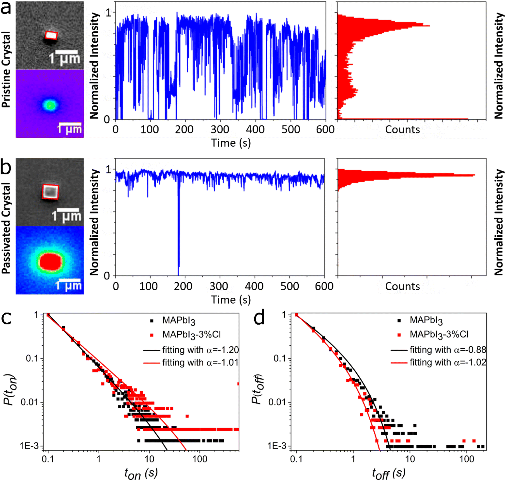 | ||
| Fig. 3 SEM and PL images, PL intensity time trajectories (10 min, 100 ms bin time) and corresponding histograms of single MAPbI3 crystals (a) before and (b) after the 3% MACl post-treatment, respectively. In the PL images, purple to red colors based on the rainbow sequence represent gradually higher intensities. Normalized probability distributions of the duration of (c) ON times and (d) OFF times of MAPbI3 NCs with 0, 3%Cl surface treatment. | ||
Fig. 3b shows a more stable PL intensity of MAPbI3-3%Cl NC and the blinking transient reveals longer “ON” durations. The SEM and PL images along with blinking trajectories of a few similar 3%, 9% and 17%Cl-treated MAPbI3 NCs are shown in Fig. S13–S15.† After thresholding (see “characterization”), truncated power-law has been fitted to the normalized probability distributions of tON/OFFs for each blinking trajectories using the formula P(tON/OFF) = A·t−α·exp(−μtON/OFF). The exponents (α) are compared to quantitatively estimate the variation of deep trap densities in single emitters.37,38 Even though drastic difference in the choice of threshold can severely affect the ON and OFF time probability distributions,39–42 using same logic for the thresholding and fitting probability distributions containing several thousands of events can be a reliable measure to probe the changes in the trap density. Fig. 3c and d show that the power-law exponents of ON-time distributions decrease from α = 1.20 to 1.01 for the pure MAPbI3 and MAPbI3-3%Cl NCs, respectively. Simultaneously, the average ON time increased from 3.16 s (in pristine) to 11.96 s after the passivation. In parallel, power-law exponents of the OFF-time distributions increase from 0.88 (pristine) to 1.02 in the MAPbI3-3%Cl crystals. The extracted ON and OFF time distribution parameters from the blinking traces (spanning 600 s at 50 mW cm−2 power density) of representative NCs after 0%, 3%, 9%, 17%Cl-passivation, are compared in Fig. S16.† The exponents of the ON-time distributions again increase and those for OFF states decreases in case of MAPbI3-9%Cl and MAPbI3-17%Cl NCs, which suggest longer OFF-durations (as observed in Fig. S13–S15†) and higher trap density with increasing Cl content and formation of MAPbCl3 on the crystal surface. In brief, MAPbI3-3%Cl NCs usually provide longest ON (shortest OFF) durations indicating lowest trap density, which is in tune with the observation under PL lifetime studies.
To further probe the heterogeneity in charge carrier dynamics of individual emitters within the ensemble, we statistically classify the blinking behavior of 67 untreated and 441 post-treated (3%, 9% and 17%) MAPbI3 crystals (%NCs ∼80%), as performed in the earlier studies.41,43 We note that intermittency characteristics of MHP emitters can be segregated among five clusters namely, (i) continuous bleaching and blinking (BB) (Fig. 4a, upper panel), (ii) initial brightening, bleaching and blinking (BBB) (Fig. S17†), (iii) multi-state blinking (MSB) (Fig. S18†), (iv) continuous photo-enhancement-blinking (PEB) (Fig. 4a, lower panel) and (v) usual quasi two-state blinking (qTSB) as shown in Fig. 3a and b (middle panel). Additionally, qTSB traces are sub-classified as “mostly on”, “intermediate” and “mostly off” emitters according to their intensity distributions (Fig. S19†).41 Intriguingly, the modal occurrence of each sub-category in the ensemble varies before and after Cl-treatment. For instance, the percentage of “mostly on” blinking under qTSB characteristic (Fig. S19†) in the entire Cl-treated population increases to 70% as compared to the untreated crystals (61%). This again indicates effective chloride-based passivation of surface defects and thus elongation of the ON durations. The number of “mostly on” emitters enhances after 3%Cl treatment (68%) which reaches a maximum (79%) for MAPbI3-9%Cl, and again goes down in case of MAPbI3-17%Cl crystals (63%). Formation of additional NR traps at the MAPbI3/Cl3 heterojunction on crystal surfaces upon intensive Cl-treatment is likely responsible for frequenting OFF-states and shortening the ON-durations, which converges with our previous observation on the power-law exponents.
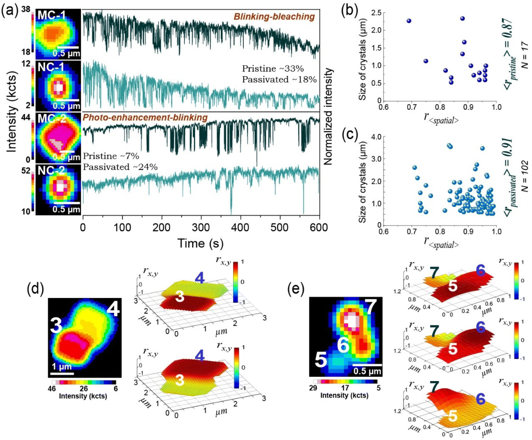 | ||
| Fig. 4 Blinking-bleaching (BB, upper panel) and photo-enhancement-blinking (PEB, lower panel) characteristic (a) for both micro- (MC-1,2) and nanocrystals (NC-1,2). Spatially averaged intra-crystal correlations (b and c) are distributed against size of the crystals considering each individual emitter. PL images of (d) two joined MCs (3, 4) and (e) three NCs (5–7) are shown with correlation maps of the entire assembly, which are constructed with respect to the average blinking characteristic of each crystal. Individual correlation maps in the upper and lower panel of (d) are made with respect to MC-3 and MC-4, respectively. The maps from top to bottom in (e) are constructed with respect to NC-5, NC-6 and NC-7, respectively. | ||
More interestingly, population of the BB characteristic (photobleaching) reduces to almost half (18%, Fig. 4a) in the Cl-treated ensemble as compared to the pristine emitters (33%). Besides, PEB (photobrightening) feature in post-treated crystals (24%) increases by more than three times with respect to the un-treated population (7%). Although %BB remains similar (22%) after 3% and 9%Cl treatment (Fig. S20†), it decreases by 45% in case of MAPbI3-17%Cl crystals. In parallel, the %PEB rises gradually with higher extent of chloride treatment (3% to 17%Cl), as depicted in the Fig. S20.† Although our investigation is irrespective of NCs and MCs, such photo-enhancement is prominent (77%) for <1 μm size Cl-treated crystals, which may be due to more uniform passivation of defects on the smaller surface area. Additionally, we find few 9% and 17%Cl-treated crystals (2%) exhibit suppressed blinking persisting up to hundreds of seconds (Fig. S21†) after certain time of photo-excitation. Sudden annihilation of blinking can be related to the persisting deactivation of NR traps/centers perhaps by structural modifications which become more feasible in presence of an excess availability of chloride ions in the intensively treated crystals. A 20–30% reduction in the population of BBB (and MSB) characteristic has been observed after Cl-post-treatment which further indicates defect passivation, preventing an overwhelming photo-induced activation of NR traps (centers) under prolonged light exposure.
In brief, iodide vacancies or under-coordinated lead atoms on the crystal surface can be compensated by performing mild MACl treatment which efficiently reduces the trap density without creating new ones and significantly stabilizes the PL intensity (Fig. 3b) with longer ON durations. A similar phenomenon was reported in MHP crystals via trap filling21,42 by an increasing excitation power. However, pristine crystals often encounter inevitable structural and optical degradation (BB emitters) under photo-exposure in the ambient condition.43 The heavy Cl-treatment (9%, 17%) on MAPbI3 NCs can lead to the formation of MAPbCl3 at the crystal surface likely due to iodide-chloride halide exchange. This potentially increases trap densities and the possibility of OFF-states due to lattice mismatch at MAPbI3/Cl3 interfaces, as shown in Fig. S22c–e (see Note 2, ESI†). Simultaneously however, intensively Cl-treated crystals exhibit higher PL intensity in bulk (Fig. 2a) and increase (decrease) the percentage of emitters showing photo-enhancement (bleaching) as shown in Fig. S20.† This may indicate MAPbCl3 often acting as a protective layer (shell) which ensures least interaction (and degradation) of the MAPbI3 crystals with the environment (O2/H2O).43 The balance between defect (NR trap) generation at MAPbI3/Cl3 interface and the longevity (or photo-enhancement) of the crystals in ambient conditions can be achieved under a mild (3%) MACl treatment to the MAPbI3 crystals.
Next, we probe the extent of charge carrier diffusion via correlating the blinking propensity of each pixel with the spatially-averaged intensity fluctuation of the entire emitter44 (Fig. S23†). This allows us to investigate carrier communication in any crystal beyond shape and dimensional constrains. The color codes have been assigned to the correlation values (rx,y) at each pixel to generate a correlation map of the crystal. It is observed that the mean spatially-averaged correlation coefficient of >100 representative Cl-post-treated (3%, 9%, 17%) NCs/MCs increases by 4.5% as compared to the untreated ensemble (Fig. 4b and c). In line with prior reports,44 we infer a lowering of the surface defect density which facilitates carrier diffusion throughout the passivated crystals. Furthermore, spatially-averaged correlation coefficient values are higher for <1 μm crystals (Fig. 4b and c) in case of both non-post-treated and post-treated ensembles. Enhanced carrier communication in smaller crystals can be assigned to a more uniform surface coverage by MACl treatment and comparable dimension of the studied NCs with carrier diffusion length (∼400 nm) of the material.45
Additionally, we investigate the photophysics of the so-called assemblies of crystals after Cl-treatment (Fig. S24†) which are presumably attached to each other by short range attractive forces46 including van der Waals attraction involving the ionic core or the ligands at the crystal surface.47–49 Such formations can be of particular interest toward thin film studies.50 As performed in previous reports,47 we compared the intermittency behavior of boundary-separated grains to understand the extent of carrier mobility in the entire assembly, which reveals that each crystal blinks distinctly, even though they are in physical proximity. This is supported by the different intermittent behavior of spatially distant nanodomains of the representative assemblies (Fig. S25†). Correlation map of the entire assembly (MC-3,4 and NC-5,6,7, Fig. 4d and e) shows a drastic fall in blinking synchronicity in individual crystals while calculated with respect to the other. Uncorrelated blinking reveals a lack of charge carrier communication beyond the grain boundaries. This can be attributed to the repulsive nature of high bandgap boundaries51,52 upon formation of MACl3 under intensive Cl treatment, which initiates energetic hindrance toward carrier diffusion (see Note 2, Fig. S22†), preserving the distinct microscopic property of each individual crystal.
As a proof of concept of the impact of trap passivation, we fabricated and characterized a photodetector (PD) using P3HT/MAPbI3 and P3HT/MAPbI3-3%Cl heterojunction films (Fig. 5a) as active layer. We have deliberately ignored the usage of MAPbI3-9%Cl and MAPbI3-17%Cl crystals to avoid any possible chance of MAPbCl3 formation and to reduce the perturbation of high energy boundaries in inter-grain carrier mobility. Fig. 5b illustrates the I–V curves of the device based on P3HT/MAPbI3 and P3HT/MAPbI3-3%Cl in dark and under weak natural light. Under natural light (30 mW cm−2), a stable drain current for the P3HT/MAPbI3-3%Cl based photodetector is obtained which is more than 5 times larger than the drain current of the P3HT/MAPbI3 based photodetector, while remaining almost zero in dark. This indicates the trap density of MAPbI3 NCs is suppressed upon 3%Cl post-treatment. The time-dependent photoresponse of the P3HT/MAPbI3 and P3HT/MAPbI3-3%Cl based PDs is summarized in Fig. 5c and d. Except for the increased photocurrent after defect passivation, a more stable photocurrent signal was achieved for the P3HT/MAPbI3-3%Cl based PDs with a rise and fall time of less than 0.1 s.
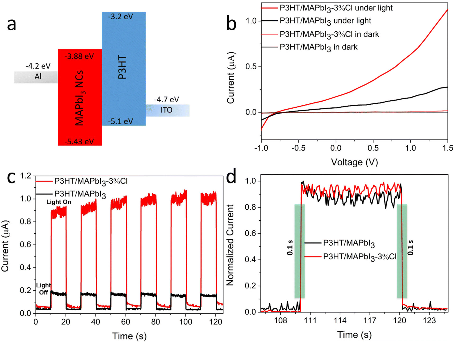 | ||
| Fig. 5 Schematic diagram of the energy levels (a) or work function of Al, MAPbI3 NCs, P3HT, and ITO in the PD devices. The current–voltage (I–V) curves (b) of the P3HT/MAPbI3 and P3HT/MAPbI3-3%Cl based PDs (device area: 0.1 cm2) in dark and under weak natural light (power density: 30 mW cm−2). Time-dependent photoresponse characteristics (c) of P3HT/MAPbI3 and P3HT/MAPbI3-3%Cl based PDs at a bias of +1 V under weak natural light. The rise (ton) and fall time (toff) (d) of P3HT/MAPbI3 and P3HT/MAPbI3-3%Cl based PDs. | ||
Conclusions
In summary, we have developed a novel approach to passivate MAPbI3 crystals by applying MACl in a mixed ethanol/toluene solvent (instead of pure polar or non-polar solvents) which efficiently suppresses surface defects while avoiding material degradation. Our results confirmed surface chloride adsorption with mild Cl content (3%) or iodide-to-chloride ion exchange under high Cl content (9% and 17%). These modifications are confined to the crystal surface without affecting the bulk of the crystals. It is found that a mild Cl concentration (3%) is the key to optimize the optical properties, as evidenced by monitoring the PL lifetime and PL blinking behavior. When only treating with a minute MACl content, a higher PLQY, longer PL lifetimes, and a longer duration of ON-states are observed, indicating the effective suppression of surface traps. However, formation of MAPbCl3 upon intense Cl-treatment often leads to unavoidable creation of additional NR traps due to lattice mismatch at the MAPbI3/Cl3 heterojunction which further extends the OFF-durations. Passivated NCs/MCs show a reduced occurrence of photobleaching as compared to the pristine ones, and even a photobrightening effect, indicating achievement of higher perovskite stability under light and ambient environment. Further, surface passivation enhances intra-crystal charge carrier diffusion to the transient (NR) recombination centers which governs spatial synchronicity in PL fluctuations of the nanodomains. However, lack of control over excessive Cl-treatment can cause formation of high bandgap MAPbCl3, especially at the defect rich boundaries. In fact, this would act as an energy barrier and perturb the inter-crystal carrier mobility/communication in the assemblies. Finally, photocurrent measurements on P3HT/MAPbI3 and P3HT/MAPbI3-3%Cl based photodetectors indicate that the P3HT/MAPbI3-3%Cl based PD exhibits a stable and more than 5 times higher photocurrent within the visible range which elucidates the effect on PV performance upon MACl post-treatment. Our findings provide a guideline for the most optimal post-treatment conditions for efficient surface defect passivation of metal halide perovskites toward more stable and efficient perovskite-based optoelectronic devices.Methods
Nanocrystal synthesis and chloride post-treatment
All the chemicals are used as received, including lead iodide (99.999%, Sigma-Aldrich), methylammonium iodide (MAI, 98%, Great cell solar materials Pty Ltd), methylammonium chloride (MACl, 98%, Sigma-Aldrich), oleylamine (OAm, 70%, technical grade, Sigma-Aldrich), TOPO (TOPO, 99%, Aldrich), poly(3-hexylthiophene-2,5-diyl) (P3HT, region-regularity = 93.6%, Ossila), acetonitrile (99.8%, Sigma-Aldrich), absolute ethanol (99.8%, Sigma-Aldrich), and toluene (ACS, Reag. Ph. Eur.).Pure MAPbI3 NCs are produced by the injection–precipitation method. The precursor solution is prepared by dissolving lead iodide (PbI2, 0.04 mmol, 18.8 mg) and methylammonium iodide (0.12 mmol, 18.8 mg) in 20 mL of acetonitrile (ACN, 99.8%). In parallel, the capping agents, 72 μL of OAm and 60 mg of TOPO, are dissolved in 30 mL toluene as antisolvent and divided into six batches after stirring. Five minutes after injection of 1.3 mL of the precursor solution into the vigorously stirred capping agent solution, an extra 7 mL of toluene is added dropwise. The mixture is kept stirring at room temperature for 4 hours at 600 rpm, resulting in a dark brown suspension containing MAPbI3 NCs. The dark brownish suspension is then washed twice with toluene after centrifugation for 30 minutes at 4200 rpm. In order to obtain a substantial yield for optical measurements, six NC batches are mixed, divided into 4 batches and re-dispersed in 4 mL of toluene. Methylammonium chloride (13.6 mg, 200 μmol) is dissolved in 0.5 mL absolute ethanol. 0, 3, 9, and 17 molar% (Cl:I molar ratio) Cl post-treatment is realized by directly adding 0, 1, 2.5 and 5 μL of the MACl solution (in ethanol), respectively, to 4 mL of the MAPbI3 NC suspension (in toluene) resulting in ethanol/toluene (v/v) ratios of 0%, 0.025%, 0.065% and 0.125%. The mixture is then kept stirring for 30 min at 600 rpm (Fig. S1†). The suspension is then washed again by centrifugation for 30 minutes at 4200 rpm, and the residue is re-dispersed in 4 mL of toluene. The final crystal suspensions are kept in the dark. SEM (scanning electron microscopy) and EDS (energy-dispersive X-ray spectroscopy) are performed by dropping 10 μl of the suspension onto a 5 mm × 5 mm silicon chip, which is dried at ambient conditions. For wide-field microscopy and time-resolved single-photon counting (TCSPC) measurements, 20 μL of the NC suspension in toluene is dropped and spin-coated at 1000 rpm for 60 s on a clean glass cover slide. Methylammonium lead chloride (MAPbCl3) is obtained via mixing an equimolar ratio of MACl and PbCl2 in DMSO (0.2 M), which is spin-coated on a clean silicon substrate and annealed at 120 °C for one hour. The MAPbI3 NCs with and without 3%Cl post-treatment for photodetector fabrication are collected through multiple syntheses and finally dried in vacuum for 12 hours.
Device fabrication
The photodetectors are constructed following an ITO/P3HT:MAPbI3 NCs (or P3HT:MAPbI3-3%Cl NCs)/Al structure. Firstly, ITO coated glass substrates are cleaned by ultra-sonication in diluted Hellmanex, ultra-pure water, acetone and isopropanol, respectively, for 30 min each and dried in a N2 flow. A 10 mg mL−1 perovskite nanocrystals dispersion in 20 mg mL−1 P3HT in toluene is spin-coated onto the ITO glass substrate at 2000 rpm for 60 s. The obtained films are then transferred onto a hot plate and annealed at 80 °C for 20 minutes. Finally, a 200 nm Al electrode is thermally evaporated on top of the P3HT/perovskite blend films. Finally, the devices are sealed by an ultraviolet-curable resin in a N2 filled glovebox.Characterization
SEM images are obtained using an FEI quanta FEG-250 environmental scanning electron microscope. X-ray diffraction (XRD) is recorded on a Malvern PANalytical Empyrean diffractometer using a Debye–Scherrer transmission geometry equipped with a PIXcel3D solid-state detector with a Cu anode. X-ray photoelectron spectroscopy (XPS) is carried out using a K-alpha Thermo spectrometer working with Al Kα radiation at 1486.68 eV. Transmission electron microscope (TEM) images are obtained using FEI Talos F2005 microscope operated at 120 kV. Energy dispersive X-ray spectroscopy measurements are recorded in STEM mode with four super energy dispersive spectroscopy (EDS) detectors. Absorption and steady-state PL spectra are measured on a Lambda 950 and an Edinburgh FLS980 with 488 nm excitation for the emission. PL blinking is recorded using the home-built integrated optical and electron microscopy system consisting of a FEI Quanta FEG-250 SEM, equipped with an inverted optical microscope (Olympus IX71) and an EM-CCD camera (Image-EM X2, Hamamatsu) for collecting the emission light.15 All the data are recorded over 6000 frames using the high-speed EM camera with an exposure time of 100 ms. The PL blinking time trace is recorded by this integrated system, before capturing the SEM morphology images. PL time traces of individual particles are extracted using a home-developed Igor super-resolution localization code. Half the intensity difference of the bright state with the subtracted background is used as the threshold to determine the ON/OFF times.21,42,53 TCSPC PL decay curves are recorded on a home-built confocal FLIM microscope with a pulsed 485 nm laser as the excitation source (1 MHz). A bandpass filter with 705–755 nm is used as the emission channel. The current–voltage (I–V) characteristic and photocurrent–response time (time interval = 0.05 s) of the photodetector in dark and under nature light (power density: 30 mW cm−2) is measured with a Keithley 2400 source meter.Conflicts of interest
The authors declare no competing financial interest.Acknowledgements
The authors acknowledge financial support from the Research Foundation – Flanders (FWO grant numbers S002019N, 1SC44719N, 1514220N, and G098319N) and for the postdoctoral fellowship to J. A. S. (FWO grant no. V400622N), the KU Leuven Research Fund (C14/19/079, iBOF-21-085 PERSIST, and STG/21/010), and the doctoral fellowship to H. J. from the China Scholarship Council (grant number 201606220032). J. H. thanks the MPI for financial support as an MPI fellow. The authors acknowledge Nagma Parveen for the Matlab code for constructing the probability graph of ON/OFF blinking.References
- Best Research-Cell Efficiencies, https://www.nrel.gov/pv/assets/pdfs/best-research-cell-efficiencies-rev220126b.pdf, (accessed: June 3, 2022).
- A. Dey, J. Ye, A. De, E. Debroye, S. K. Ha, E. Bladt, A. S. Kshirsagar, Z. Wang, J. Yin, Y. Wang, L. N. Quan, F. Yan, M. Gao, X. Li, J. Shamsi, T. Debnath, M. Cao, M. A. Scheel, S. Kumar, J. A. Steele, M. Gerhard, L. Chouhan, K. Xu, X.-g. Wu, Y. Li, Y. Zhang, A. Dutta, C. Han, I. Vincon, A. L. Rogach, A. Nag, A. Samanta, B. A. Korgel, C.-J. Shih, D. R. Gamelin, D. H. Son, H. Zeng, H. Zhong, H. Sun, H. V. Demir, I. G. Scheblykin, I. Mora-Seró, J. K. Stolarczyk, J. Z. Zhang, J. Feldmann, J. Hofkens, J. M. Luther, J. Pérez-Prieto, L. Li, L. Manna, M. I. Bodnarchuk, M. V. Kovalenko, M. B. J. Roeffaers, N. Pradhan, O. F. Mohammed, O. M. Bakr, P. Yang, P. Müller-Buschbaum, P. V. Kamat, Q. Bao, Q. Zhang, R. Krahne, R. E. Galian, S. D. Stranks, S. Bals, V. Biju, W. A. Tisdale, Y. Yan, R. L. Z. Hoye and L. Polavarapu, ACS Nano, 2021, 15, 10775–10981 CrossRef CAS PubMed.
- S. Rühle, Sol. Energy, 2016, 130, 139–147 CrossRef.
- Y. Yang and J. You, Nature, 2017, 544, 155–156 CrossRef CAS PubMed.
- H. Jin, E. Debroye, M. Keshavarz, I. G. Scheblykin, M. B. Roeffaers, J. Hofkens and J. A. Steele, Mater. Horiz., 2020, 7, 397–410 RSC.
- D. Meggiolaro, S. G. Motti, E. Mosconi, A. J. Barker, J. Ball, C. A. R. Perini, F. Deschler, A. Petrozza and F. De Angelis, Energy Environ. Sci., 2018, 11, 702–713 RSC.
- A. Abate, M. Saliba, D. J. Hollman, S. D. Stranks, K. Wojciechowski, R. Avolio, G. Grancini, A. Petrozza and H. J. Snaith, Nano Lett., 2014, 14, 3247–3254 CrossRef CAS.
- S. Yang, S. Chen, E. Mosconi, Y. Fang, X. Xiao, C. Wang, Y. Zhou, Z. Yu, J. Zhao and Y. Gao, Science, 2019, 365, 473–478 CrossRef CAS PubMed.
- B. R. Sutherland, Joule, 2017, 1, 423–424 CrossRef CAS.
- Q. Wang, B. Chen, Y. Liu, Y. Deng, Y. Bai, Q. Dong and J. Huang, Energy Environ. Sci., 2017, 10, 516–522 RSC.
- G. Nan, X. Zhang, M. Abdi-Jalebi, Z. Andaji-Garmaroudi, S. D. Stranks, G. Lu and D. Beljonne, Adv. Energy Mater., 2018, 8, 1702754 CrossRef.
- N. K. Noel, A. Abate, S. D. Stranks, E. S. Parrott, V. M. Burlakov, A. Goriely and H. J. Snaith, ACS Nano, 2014, 8, 9815–9821 CrossRef CAS PubMed.
- T. Hwang, A. J. Yun, B. Lee, J. Kim, Y. Lee and B. Park, J. Appl. Phys., 2019, 126, 023101 CrossRef.
- M. Li, X. Yan, Z. Kang, Y. Huan, Y. Li, R. Zhang and Y. Zhang, ACS Appl. Mater. Interfaces, 2018, 10, 18787–18795 CrossRef CAS PubMed.
- H. Jin, J. A. Steele, R. Cheng, N. Parveen, M. B. Roeffaers, J. Hofkens and E. Debroye, Adv. Opt. Mater., 2021, 9, 2002240 CrossRef CAS.
- D.-Y. Son, J.-W. Lee, Y. J. Choi, I.-H. Jang, S. Lee, P. J. Yoo, H. Shin, N. Ahn, M. Choi, D. Kim and N.-G. Park, Nat. Energy, 2016, 1, 16081 CrossRef CAS.
- M. I. Saidaminov, J. Kim, A. Jain, R. Quintero-Bermudez, H. Tan, G. Long, F. Tan, A. Johnston, Y. Zhao, O. Voznyy and E. H. Sargent, Nat. Energy, 2018, 3, 648–654 CrossRef CAS.
- A. Kogo and M. Chikamatsu, Chem. Commun., 2020, 56, 1235–1238 RSC.
- N. Aristidou, C. Eames, I. Sanchez-Molina, X. Bu, J. Kosco, M. S. Islam and S. A. Haque, Nat. Commun., 2017, 8, 15218 CrossRef PubMed.
- Y. Lin, J. Lim, L. Aspitarte, K. Sharma, P. Madhu, A. Morales-Vilches, P. Nayak, S. Bai, F. Gao, C. Grovenor, Y. Lin, N. Sakai, P. Da, J. Wu, H. Sansom, A. Ramadan, S. Mahesh, J. Liu, R. D. J. Oliver, J. Lim, L. Aspitarte, K. Sharma, P. K. Madhu, A. B. Morales-Vilches, P. K. Nayak, S. Bai, F. Gao, C. R. M. Grovenor, M. B. Johnston, J. G. Labram, J. R. Durrant, J. M. Ball, B. Wenger, B. Stannowski and H. J. Snaith, Science, 2020, 369, 96–102 CrossRef CAS PubMed.
- Y. Tian, A. Merdasa, M. Peter, M. Abdellah, K. Zheng, C. S. Ponseca Jr., T. n. Pullerits, A. Yartsev, V. Sundström and I. G. Scheblykin, Nano Lett., 2015, 15, 1603–1608 CrossRef CAS PubMed.
- H. Yuan, E. Debroye, E. Bladt, G. Lu, M. Keshavarz, K. P. Janssen, M. B. Roeffaers, S. Bals, E. H. Sargent and J. Hofkens, Adv. Mater., 2018, 30, 1705494 CrossRef PubMed.
- A. Merdasa, Y. Tian, R. Camacho, A. Dobrovolsky, E. Debroye, E. L. Unger, J. Hofkens, V. Sundström and I. G. Scheblykin, ACS Nano, 2017, 11, 5391–5404 CrossRef CAS PubMed.
- S. T. Ha, X. Liu, Q. Zhang, D. Giovanni, T. C. Sum and Q. Xiong, Adv. Opt. Mater., 2014, 2, 838–844 CrossRef CAS.
- H. Bhatia, J. A. Steele, C. Martin, M. Keshavarz, G. Solis-Fernandez, H. Yuan, G. Fleury, H. Huang, I. Dovgaliuk, D. Chernyshov, J. Hendrix, M. B. J. Roeffaers, J. Hofkens and E. Debroye, Chem. Mater., 2019, 31, 6824–6832 CrossRef CAS.
- E. Debroye, H. Yuan, E. Bladt, W. Baekelant, M. Van der Auweraer, J. Hofkens, S. Bals and M. B. Roeffaers, ChemNanoMat, 2017, 3, 223–227 CrossRef CAS PubMed.
- Q. Jiang, Y. Zhao, X. Zhang, X. Yang, Y. Chen, Z. Chu, Q. Ye, X. Li, Z. Yin and J. You, Nat. Photonics, 2019, 13, 460–466 CrossRef CAS.
- E. L. Unger, A. R. Bowring, C. J. Tassone, V. L. Pool, A. Gold-Parker, R. Cheacharoen, K. H. Stone, E. T. Hoke, M. F. Toney and M. D. McGehee, Chem. Mater., 2014, 26, 7158–7165 CrossRef CAS.
- P. Nandi, C. Giri, D. Swain, U. Manju and D. Topwal, CrystEngComm, 2019, 21, 656–661 RSC.
- B. Conings, L. Baeten, C. De Dobbelaere, J. D'Haen, J. Manca and H. G. Boyen, Adv. Mater., 2014, 26, 2041–2046 CrossRef CAS PubMed.
- J. D. McGettrick, K. Hooper, A. Pockett, J. Baker, J. Troughton, M. Carnie and T. Watson, Mater. Lett., 2019, 251, 98–101 CrossRef CAS.
- X. Zheng, B. Chen, J. Dai, Y. Fang, Y. Bai, Y. Lin, H. Wei, X. C. Zeng and J. Huang, Nat. Energy, 2017, 2, 1–9 Search PubMed.
- H. Kumar, A. Kumari and R. R. Singh, Opt. Mater., 2017, 69, 23–29 CrossRef CAS.
- X. Gu, W. Xiang, Q. Tian and S. Liu, Angew. Chem., Int. Ed., 2021, 60(43), 23164–23170 CrossRef CAS PubMed.
- Y. Liu, H. Lu, J. Niu, H. Zhang, S. Lou, C. Gao, Y. Zhan, X. Zhang, Q. Jin and L. Zheng, AIP Adv., 2018, 8, 095108 CrossRef.
- M. Jung, T. J. Shin, J. Seo, G. Kim and S. I. Seok, Energy Environ. Sci., 2018, 11, 2188–2197 RSC.
- C. Galland, Y. Ghosh, A. Steinbrück, M. Sykora, J. A. Hollingsworth, V. I. Klimov and H. Htoon, Nature, 2011, 479, 203–207 CrossRef CAS PubMed.
- L. Chouhan, S. Ito, E. M. Thomas, Y. Takano, S. Ghimire, H. Miyasaka and V. Biju, ACS Nano, 2021, 15(2), 2831–2838 CrossRef CAS PubMed.
- Y. J. Bae, N. A. Gibson, T. X. Ding, A. P. Alivisatos and S. R. Leone, J. Phys. Chem. C, 2016, 120, 29484–29490 CrossRef CAS.
- X. Wen, A. Ho-Baillie, S. Huang, R. Sheng, S. Chen, H.-c. Ko and M. A. Green, Nano Lett., 2015, 15, 4644–4649 CrossRef CAS PubMed.
- A. Mukherjee, K. K. Ray, C. Phadnis, A. Layek, S. Bera and A. Chowdhury, J. Chem. Phys., 2019, 151, 084701 CrossRef PubMed.
- H. Yuan, E. Debroye, G. Caliandro, K. P. Janssen, J. Van Loon, C. E. Kirschhock, J. A. Martens, J. Hofkens and M. B. Roeffaers, ACS Omega, 2016, 1, 148–159 CrossRef CAS PubMed.
- A. Mukherjee, M. Roy, N. Pathoor, M. Aslam and A. Chowdhury, J. Phys. Chem. C, 2021, 125, 17133–17143 CrossRef CAS.
- N. Pathoor, A. Halder, A. Mukherjee, J. Mahato, S. K. Sarkar and A. Chowdhury, Angew. Chem., Int. Ed., 2018, 57, 11603–11607 CrossRef CAS PubMed.
- G. W. Adhyaksa, L. W. Veldhuizen, Y. Kuang, S. Brittman, R. E. Schropp and E. C. Garnett, Chem. Mater., 2016, 28, 5259–5263 CrossRef CAS.
- M. A. Boles, M. Engel and D. V. Talapin, Chem. Rev., 2016, 116, 11220–11289 CrossRef CAS.
- W. Xu, W. Liu, J. F. Schmidt, W. Zhao, X. Lu, T. Raab, C. Diederichs, W. Gao, D. V. Seletskiy and Q. Xiong, Nature, 2017, 541, 62–67 CrossRef CAS PubMed.
- J. Liu, X. Zheng, O. F. Mohammed and O. M. Bakr, Acc. Chem. Res., 2022, 55, 262–274 CrossRef CAS PubMed.
- Y. Liu, M. Siron, D. Lu, J. Yang, R. Dos Reis, F. Cui, M. Gao, M. Lai, J. Lin and Q. Kong, J. Am. Chem. Soc., 2019, 141, 13028–13032 CrossRef CAS PubMed.
- M. A. Green, A. Ho-Baillie and H. J. Snaith, Nat. Photonics, 2014, 8, 506–514 CrossRef CAS.
- R. Gegevičius, M. Franckevičius and V. Gulbinas, Eur. J. Inorg. Chem., 2021, 2021, 3519–3527 CrossRef.
- J.-W. Lee, S.-H. Bae, N. De Marco, Y.-T. Hsieh, Z. Dai and Y. Yang, Mater. Today Energy, 2018, 7, 149–160 CrossRef.
- B. Rogez, H. Yang, E. Le Moal, S. Lévêque-Fort, E. Boer-Duchemin, F. Yao, Y.-H. Lee, Y. Zhang, K. D. Wegner, N. Hildebrandt, A. Mayne and G. Dujardin, J. Phys. Chem. C, 2014, 118, 18445–18452 CrossRef CAS.
- H. Bhatia, C. Martin, M. Keshavarz, I. Dovgaliuk, N.J. Schrenker, M. Ottesen, W. Qiu, E. Fron, M. Bremholm, J. Van de Vondel, S. Bals, M.B.J. Roeffaers, J. Hofkens and E. Debroye, ACS Appl. Mater. Interfaces, 2023, 15(5), 7294–7307 CrossRef CAS PubMed.
Footnotes |
| † Electronic supplementary information (ESI) available. See DOI: https://doi.org/10.1039/d2nr06427h |
| ‡ These authors contributed equally. |
| This journal is © The Royal Society of Chemistry 2023 |