
Achieving adjustable digital-to-analog conversion in memristors with embedded Cs2AgSbBr6 nanoparticles†
Yuchan
Wang‡
 *,
Nannan
Xu‡
,
Yiming
Yuan
,
Wenxia
Zhang
*,
Qiang
Huang
,
Xiaosheng
Tang
and
Fei
Qi
*
*,
Nannan
Xu‡
,
Yiming
Yuan
,
Wenxia
Zhang
*,
Qiang
Huang
,
Xiaosheng
Tang
and
Fei
Qi
*
Optoelectronic Engineering, Chongqing University of Posts and Telecommunications, Chongqing 400065, China. E-mail: yuchanwang87@163.com; zhangwx@cqupt.edu.cn; qifei@cqupt.edu.cn
First published on 28th March 2023
Abstract
In this work, the proportions of Cs2AgSbBr6 nanoparticles (NPs) mixed in a PMMA film are adjusted to the digital and analog types of resistive switching (RS) behaviors in Ag/PMMA&Cs2AgSbBr6-NPs/ITO memristor devices. It is confirmed that when the concentration of NPs doped in the PMMA film is about 5 wt%, the memristor devices demonstrate bipolar digital RS behaviors with excellent electrical characteristics such as low operating voltage, high ON/OFF ratio (>500), good endurance (>800 cycles), and stable retention ability (>104 s). However, the devices showed a transition to analog-type memristive behavior when the concentration of NPs doped in the PMMA film is around 10 wt%, and several artificial synapse behaviors are successfully simulated. The device model simulation is also used to explore the effect of the NPs on the local electric field and growing filaments. Our work provides an opportunity to explore next-generation artificial synapse devices based on lead-free halide perovskites.
Introduction
Typically, memristors based on the resistive switching (RS) effect are divided into digital and analog types.1–3 Digital memristors exhibit an abrupt change in resistance switching when writing or erasing data, and are regarded as the most promising candidate for next-generation non-volatile memory devices owing to their advantages of simple structure, fast switching speed, and low power consumption.4–6 Analog-type memristors with a gradual resistance change have attracted extensive attention in the fields of artificial synapse devices, brain-like neuromorphic computing chips, and analog non-volatile memories.7Analog-type memristors not only can realize non-volatile information storage but also can simulate the synaptic behavior.8 Therefore, it is important for the memristor devices to achieve the conversion from digital-type to analog-type in a simple way.9 Several attempts have been made to obtain the conversion. Li et al. reported that the digital-to-analog conversion in TaOx-based devices was achieved by changing the top electrode materials.10 Saleem et al. reported on the addition of a TiW barrier layer between the top electrode and the switching layer to obtain the digital-to-analog conversion.11 However, such approaches require changes in device structure and materials, which have increased the complexity of device fabrication.
Poly(methyl methacrylate) (PMMA) is a dielectric polymer with low cost, high transparency, and easy processing, which has received widespread attention in electronic devices.12 Several efforts have been attempted to explore effective methods to obtain improved RS performance due to the modified local electric field by doping nanoparticles (NPs) into the dielectric layer.13–16 Very recently, the all-inorganic lead halide perovskites have been widely adopted in memristor devices owing to its easy fabrication, high carrier mobility, and long carrier diffusion length.17 Nevertheless, the toxicity of the Pb element to humans and the environment has restricted its further development. One of the most effective ways is to replace the Pb element with the combined monovalent cations (Ag+, Cu+) and trivalent cations (Bi3+, Sb3+) in a double perovskite structure.18 However, there is still a lack of reports on the modulation of the RS performance by lead-free perovskite NPs. Therefore, a feasible way to improve the RS properties is by embedding lead-free perovskite NPs in the PMMA layers, and it should be intensively investigated as a further step.
Herein, an adjustable digital-to-analog conversion method in memristors is proposed by embedding Cs2AgSbBr6-NPs in the PMMA layer. The RS performances of the Ag/PMMA&Cs2AgSbBr6-NPs/indium-tin-oxide (ITO) memristor devices with different concentrations of Cs2AgSbBr6-NPs were thoroughly investigated, and it was demonstrated that the Cs2AgSbBr6-NPs play a crucial role in the RS behavior. It is confirmed that when the concentration of NPs doped in the PMMA film is about 5 wt%, the memristor devices demonstrated bipolar digital RS behaviors with excellent electrical characteristics such as low operating voltage, high ON/OFF ratio (>500), good endurance (>800 cycles), stable retention ability (>104 s), and more uniform switching voltages. Whereas, when the concentration of the NPs doped in the PMMA film is around 10 wt%, the memristors switch to continuously adjustable resistance states and several artificial synapse behaviors are successfully simulated. More importantly, the effect of NPs is explored through the device model simulation, which suggests that the improved RS performance and the adjustable digital-to-analog conversion behavior are attributed to the local electric field and growing filaments affected by the added NPs. Our study will pave a new way for designing and fabricating the next-generation artificial synapse devices based on lead-free halide perovskites.
Results and discussion
The X-ray diffraction (XRD) peaks of the as-synthesized Cs2AgSbBr6-NPs powders drop cast on a glass slide are observed at 15.6°, 22.2°, 27.3°, 31.7°, 39.2°, 45.7°, and 56.2°, which correspond to the (002), (022), (222), (004), (224), (044) and (444) crystal planes, respectively, confirming the cubic structure of the Cs2AgSbBr6 crystal in Fig. 1a.17 As shown in Fig. 1b, the transmission electron microscopy (TEM) images reveal the morphology of the Cs2AgSbBr6-NPs with diameters ranging from 5–10 nm, displaying a relatively uniform dispersed distribution. Clearly visible lattice fringes of the Cs2AgSbBr6-NPs measured by high-resolution TEM (HRTEM) images exhibit the inter-planar distances of about 0.165 nm and 0.206 nm, corresponding to the (444) and (044) planes of the Cs2AgSbBr6 crystal, respectively. Fig. S1a† presents the absorption spectra of Cs2AgSbBr6-NPs, where a sharp peak at 460 nm is visible. Fig. S1b† shows the transmission spectra of the PMMA film embedded with Cs2AgSbBr6-NPs. The material displays high transparency to visible light, indicating a good advantage in transparent device applications. The PMMA&Cs2AgSbBr6-NPs films prepared by the spin-coating method show dense and uniform features, as obtained by the top-view scanning electron microscope (SEM) image (Fig. 1c). The cross-sectional SEM image of the fabricated devices demonstrates that the thickness of the PMMA&Cs2AgSbBr6-NPs layer is about 110 nm, whereas the thicknesses of the top Ag and bottom ITO electrodes are around 125 nm and 230 nm, respectively (Fig. 1d). The corresponding schematic diagram of the sandwich-like device structure is illustrated in Fig. 1e.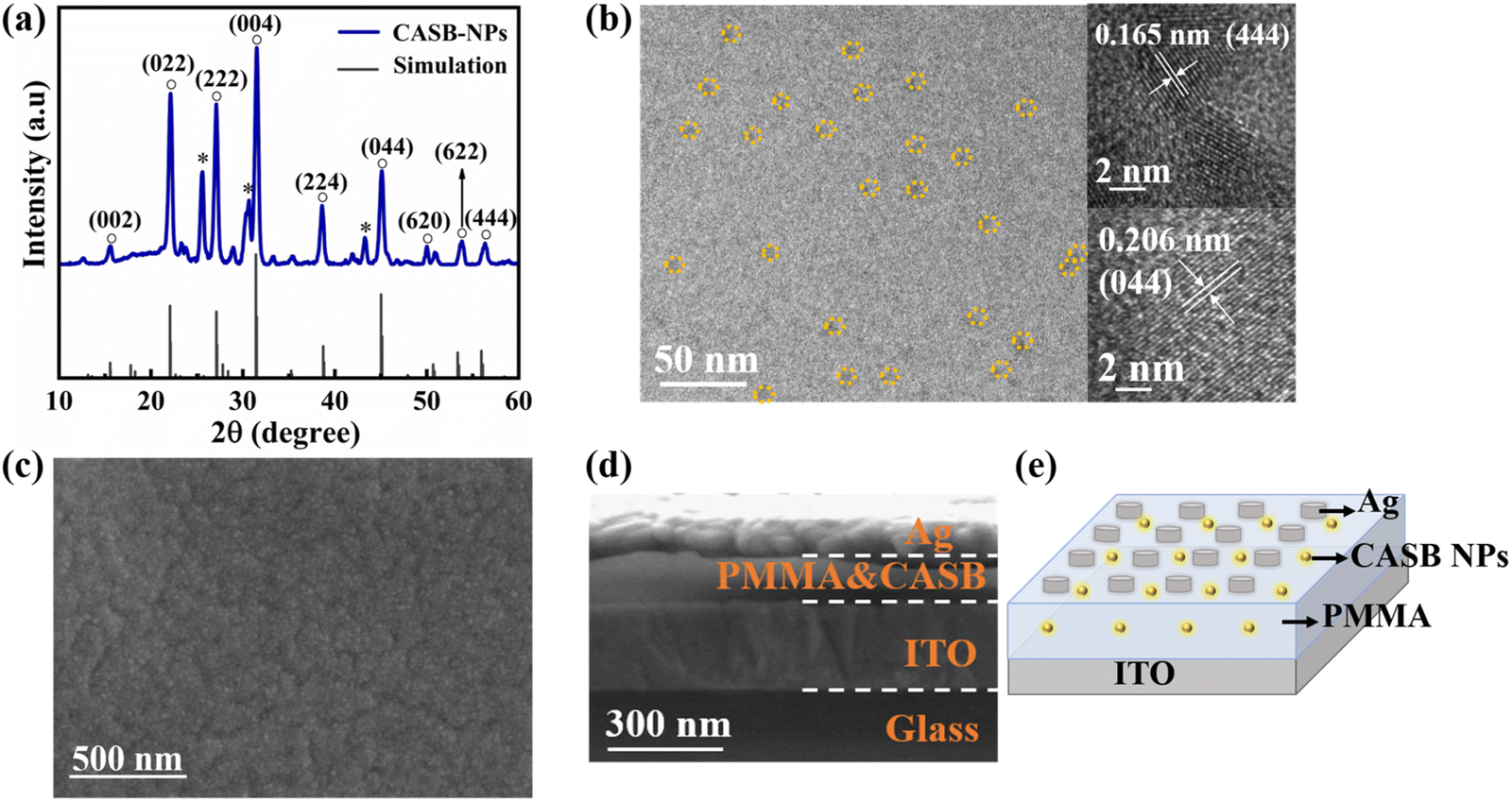 | ||
| Fig. 1 (a) The XRD patterns of the Cs2AgSbBr6(CASB)-NPs powders. * indicates the peak of incompletely dissolved AgBr. (b) The TEM image of Cs2AgSbBr6-NPs and the HRTEM images of typical nanoparticles with clearly visible lattice fringes. (c) The top-view SEM image of the PMMA&Cs2AgSbBr6-NPs thin film. (d) The cross-sectional SEM image and (e) the corresponding schematic diagram of the Ag/PMMA&Cs2AgSbBr6-NPs/ITO memristor device. | ||
To investigate the interaction of the different Cs2AgSbBr6-NPs concentrations on the electrical characteristics of the memristors, the direct current (DC) voltage sweeps were conducted for the memristor devices with NPs concentrations of 0%, 1%, 3%, 5%, and 10%, as shown in Fig. 2a–e. The applied voltage bias is connected to the Ag top electrode through a tungsten probe, and the ITO electrode is grounded. The voltage sweep is looped as 0 → 2 V → 0 V → −4 V → 0 V, and a compliance current of 1 mA is added to the positive cycle to prevent irreversible breakdown. The switching from the high resistance state (HRS) to the low resistance state (LRS) occurs during the positive sweep (set process), while the memristors turn back from the LRS to the HRS under the negative sweep (reset process). During the DC scan, the point at which the current value starts to rise is recognized as the set voltage (Vset), while the point where the current value starts to drop is recognized as the reset voltage (Vreset). From the I–V curves, it can be seen that the 0%–5% NPs devices present an abrupt current change of the digital-type. Nevertheless, the change in current gradually becomes slower and exhibits an analog-type in the set process when 10% NPs are added to the device. The five memristors are statistically shown in Fig. 2f with 50 random I–V curves per group for the set and reset voltages. The mean value of the set/reset voltage for the 0%, 1%, 3%, 5% and 10% Cs2AgSbBr6-NPs memristors are 1.06 V/−0.81 V, 0.77 V/−0.49 V, 0.68 V/−0.58 V, 0.67 V/−0.42 V and 0.68 V/−0.66 V, respectively, indicating that the RS properties are gradually improved with the increasing NPs concentration from 0% to 5%. As the concentration rises to 10%, the reset voltage of the device significantly increases. Among the results, the 5% NPs memristor devices showed the lowest and most uniform programming voltage, exhibiting the potential of high-performance digital RS memory.
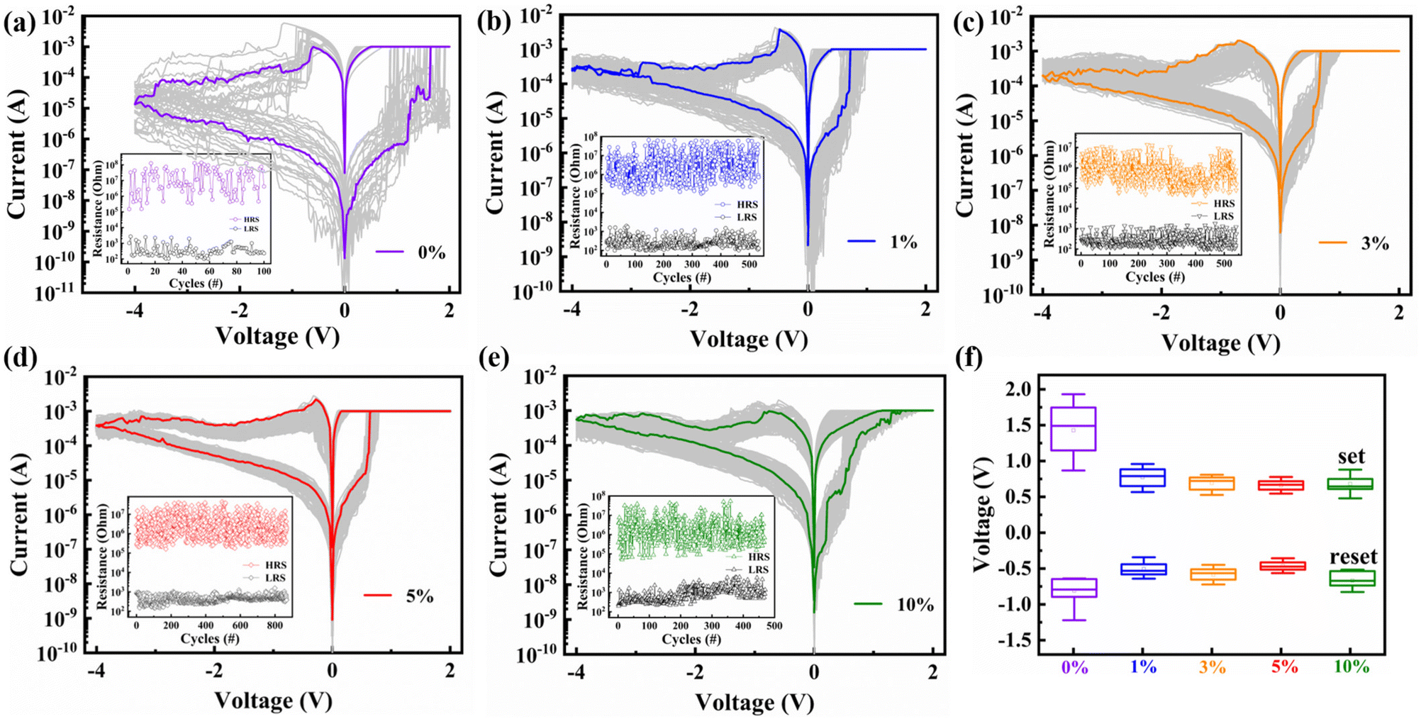 | ||
| Fig. 2 The I–V curves of the Ag/PMMA&Cs2AgSbBr6-NPs/ITO memristors for the embedded Cs2AgSbBr6-NPs in PMMA layer are (a) 0%, (b) 1%, (c) 3%, (d) 5% and (e) 10%, respectively. The voltage calculated for HRS and LRS is 0.1 V. (f) The variations of the set and reset voltages of the five memristors. | ||
The statistical analysis was performed to evaluate the reliability of the device by analyzing the switching voltage and HRS/LRS values. The cycle-to-cycle (C-to-C) and device-to-device (D-to-D) variations of the 5% Cs2AgSbBr6-NPs devices were firstly investigated, and are shown in Fig. 3a and b. The set/reset voltages and the ON/OFF ratio for the 5% Cs2AgSbBr6-NPs devices were retained with almost no fluctuations in the C-to-C and D-to-D variations. The mean reset/set voltage values of the C-to-C and D-to-D devices are −0.47 V/0.71 V and −0.46 V/0.68 V, respectively, which are quite low. The insets of Fig. 3a and b are the histograms of the C-to-C and D-to-D devices, with the mean HRS/LRS values of 5.22 MΩ/582.8 Ω and 3.43 MΩ/305.8 Ω, respectively. Subsequently, the data retention ability of the Ag/PMMA&Cs2AgSbBr6-NPs (5%)/ITO device was evaluated, as shown in Fig. S2.† The ON/OFF ratio of the device is large enough to exceed 500, and remained over 104 s.
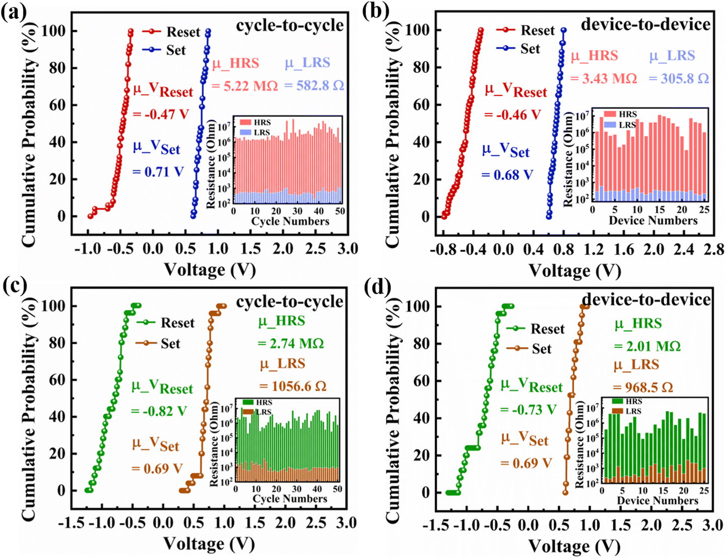 | ||
| Fig. 3 Cumulative probability distributions of Vreset/Vset for (a) C-to-C variation and (b) D-to-D variation of the Ag/PMMA&Cs2AgSbBr6-NPs (5%)/ITO device. Cumulative probability distributions of Vreset/Vset for the (c) C-to-C variation and (d) D-to-D variation of the Ag/PMMA&Cs2AgSbBr6-NPs (10%)/ITO device. The insets are the histograms of HRS/LRS of the devices. | ||
In addition, the same statistical analysis is applied to 10% Cs2AgSbBr6-NPs devices, as shown in Fig. 3c and d. The mean reset/set voltage values of C-to-C and D-to-D are −0.82 V/0.69 V and −0.73 V/0.69 V, and the mean HRS/LRS values are 2.74 MΩ/1056.6 Ω and 2.01 MΩ/968.5 Ω. It is obvious that the HRS and reset voltage are larger than that of the 5% Cs2AgSbBr6-NPs devices. This may be attributed to the insufficient disconnection of the conductive path in the HRS region, resulting in increased resistance and switching voltage.
A typical metal–semiconductor–metal sandwich structure is usually proposed to simulate the operation process of artificial synapses.19 One of the electrodes acts as the pre-synaptic neuron. When the voltage pulse is applied to the pre-synaptic neuron, the CFs are formed in the active layer, which is prepared for charge carrier transport and allows the neurotransmitter transmission into the synaptic gap (Fig. 4a). Another electrode serves the role of the post-synaptic neuron that receives neurotransmitters across the synaptic gap. To demonstrate the artificial synaptic behavior of the prepared memristors, the consecutive dual sweeps of voltage (0 V → 0.2 V → 0 V → −1.0 V → 0 V) are applied to the Ag/PMMA&Cs2AgSbBr6-NPs (10%)/ITO device. It was observed that the device resistance gradually decreased (increased) with consecutive positive (negative) sweeping voltage changes, rather than suddenly changes (Fig. 4b). The results indicate that the PMMA&Cs2AgSbBr6-NPs(10%) memristors display continuously adjustable resistance in the DC mode, which manifests a potential to emulate biological synapses.
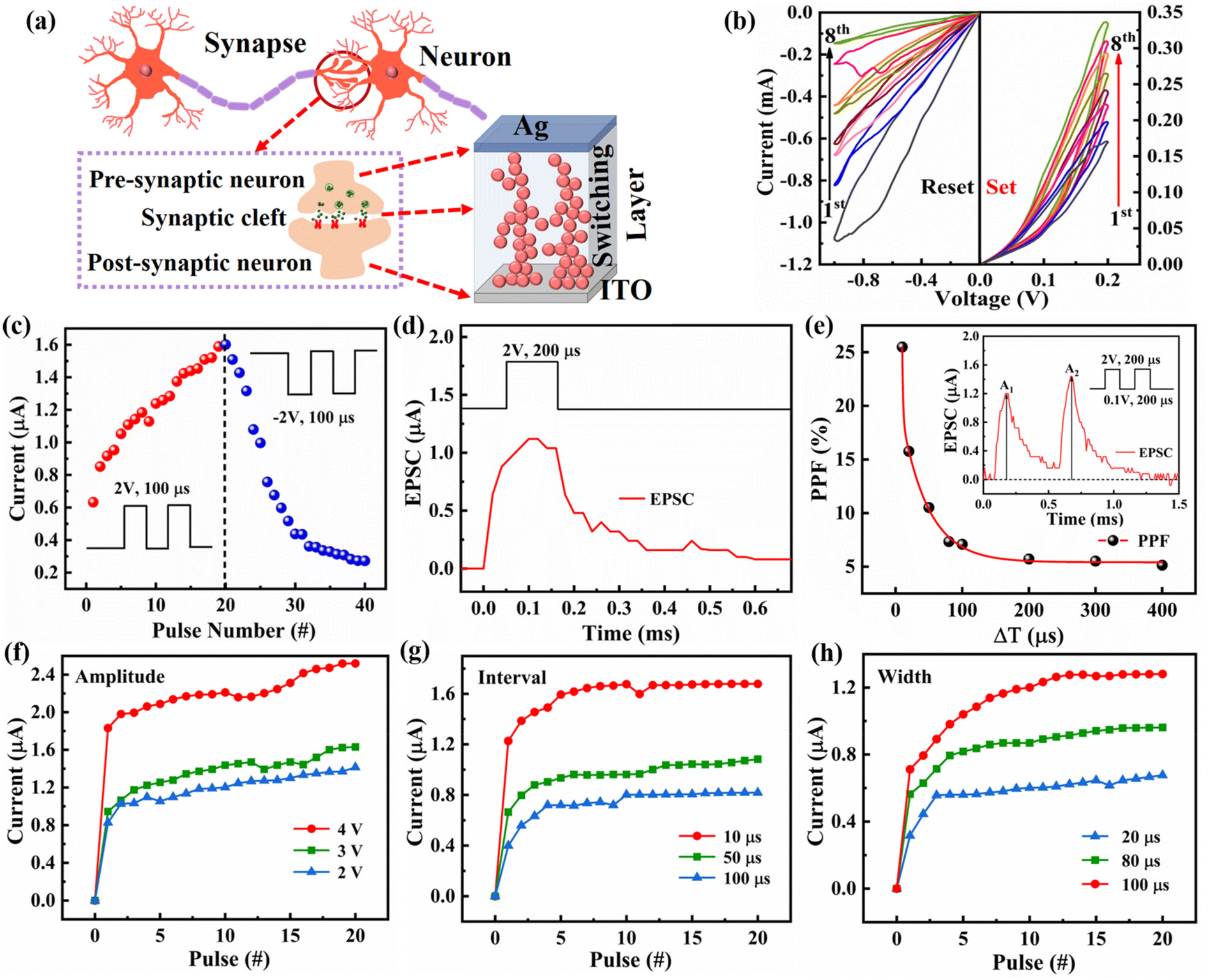 | ||
| Fig. 4 (a) Schematic illustration of the biological neurons and synapses using the Ag/PMMA&Cs2AgSbBr6-NPs (10%)/ITO memristor device. (b) The I–V curves under 8 positive and 8 negative dual voltage sweeps. (c) The current change of the memristor devices under the influence of the positive and negative pulses. (d) The EPSC triggered by a single pre-synaptic spike (2 V, 200 μs) in the Cs2AgSbBr6-NPs based memristor device. (e) Variation of the PPF index with different interval time (ΔT) of two consecutive voltage pulses; the inset shows the EPSC triggered by a pair of pre-synaptic spikes (2 V, 200 μs). The dependence between the conducting current and pulse (f) amplitude, (g) interval, and (h) width. | ||
To further demonstrate the continuously adjustable conductance under AC pulses, the resistance variations of the memristors under 20 positive pulses (2 V, 100 μs) and 20 negative pulses (−2 V, 100 μs) are shown in Fig. 4c. Similar to the results under DC sweep, the resistance of the memristor increases or decreases with the increasing number of positive or negative pulses, respectively. It implies that the conductance of the memristors can be adjusted by the input pulse voltage, which can be employed to simulate the biological synapse behavior to perceive and memorize the excitation and inhibition. To further evaluate the synaptic behavior of the memristors, the experimental setup shown in Fig. S3† is used to accomplish the pulse measurement. When a single pre-synaptic spike (2 V, 200 μs) is applied to the memristor (0.1 V reading voltage to detect the device state), the device current rises sharply after the pulse stimulation and decays gradually to zero as time passes after the voltage is withdrawn (Fig. 4d). This phenomenon is consistent with the excitatory post-synaptic current (EPSC) behavior of biological synapses. When two pre-synaptic spikes are applied continuously, the second EPSC value (A2) is higher than the first value (A1), which refers to the paired pulse facilitation (PPF). The PPF index is calculated from the following equation:
| PPF index = (A2 − A1)/A1 × 100%. | (1) |
The interval time between the two applied consecutive pulses will determine the magnitude of the synaptic facilitation index. As shown in Fig. 4e, the PPF index decreased from 25.7% to 5.3% when ΔT of the paired pulse increased from 10 μs to 400 μs. The data can be well matched to the double exponential decay function as follows:20
y = y0 + C1![[thin space (1/6-em)]](https://www.rsc.org/images/entities/char_2009.gif) exp(−ΔT/τ1) + C2exp(−ΔT/τ2) exp(−ΔT/τ1) + C2exp(−ΔT/τ2) | (2) |
It is well known that filamentary conduction mechanisms are widely used to explain the resistance change in RS devices, which are classified into two types, including the electrochemical metallization mechanism (ECM) originating from active electrodes and valence change mechanism (VCM) originating from the intrinsic defects of the switching materials.21,22 The repeated ON/OFF operation in the RS devices based on Ag electrodes is usually considered as the rupture and growth of Ag metal CFs, which are formed by the stacking of Ag+ cations in the switching layer. To verify this, devices with different electrode sizes were examined for resistance fluctuations, as shown in Fig. S4a,† since the filamentary conduction would not vary with the device interface area.23,24 Due to little variation in the device resistance, the PMMA&Cs2AgSbBr6-NPs based devices are considered to have a filamentary conduction mechanism. Next, the electrical properties of the Au electrode devices were tested under the same conditions to investigate the dominant type of switching modes (Fig. S4b†). It was shown that the RS behavior of the Ag/PMMA&Cs2AgSbBr6-NPs/ITO devices mainly accounted for the ECM mode with Ag-CFs since no obvious RS phenomenon was observed in the Au/PMMA&Cs2AgSbBr6-NPs/ITO devices.24,25
To further investigate the carrier transport mechanism of the fabricated memristors, the I–V curve is replotted on a double logarithmic scale, as shown in Fig. S4c and d.† In the HRS region under positive bias, the conduction mechanism is firstly followed by ohmic behavior (I ∝ V), where the number of the thermally excited carriers is more than the number of injected carriers and the traps are partially filled. As the voltage grows, the injected carriers rapidly increase and occupy the traps, indicating a space-charge-limited conduction (SCLC) mechanism (I ∝ Vn, n ≥ 2). Once the traps have been fully filled, the carriers move easily through the dielectric layer, resulting in a sudden rise of current. With the formation of Ag-CFs across the switching layer, the resistance is switched to LRS and the mechanism obeys the ohmic conduction. When the electric field polarity is converted, the carriers come out of the trap centers, causing the resistance to switch from LRS to HRS, and the mechanism switches from SCLC to ohmic behavior.26
To find out how the Cs2AgSbBr6-NPs affects the device performance, a two-dimensional finite analysis using COMSOL Multiphysics was used to analyze the electric fields of the memristor devices with and without Cs2AgSbBr6-NPs in the active layer. The simulation was performed with a transient process of 1 ns (Fig. S5†). It should be noted that the CFs are considered to be formed predominantly by the stacking of Ag atoms; thus, the material parameters of silver are adopted. As shown in Fig. 5a and b, the memristor devices in the HRS are introduced to explain the mechanism of CF growth during the set process. It can be clearly observed that the local electric field is quite weak in the model without NPs addition. Meanwhile, in the NPs-doped model, the local electric field is significantly enhanced especially near the CF rupture. Moreover, the CF tip is linked along the NPs, leading to the enhanced electric field channels up to the bottom electrodes. The Cs2AgSbBr6-NPs act as trap centers for charge trapping or release in the PMMA thin films.27 When the positive voltage is applied, the probability of the injected carriers getting trapped increases, which implies that more Ag+ cations are reduced to Ag atoms by combination with electrons due to the addition of the NPs. The schematic diagram of the generation and breakage of the conductive filament in a digital memristor is shown in Fig. S6.† The oxygen vacancies in the PMMA dielectric layer have a modulation effect and provide enough space for Ag-CFs formation, allowing the filaments to grow uniformly along the position of the Cs2AgSbBr6-NPs.28
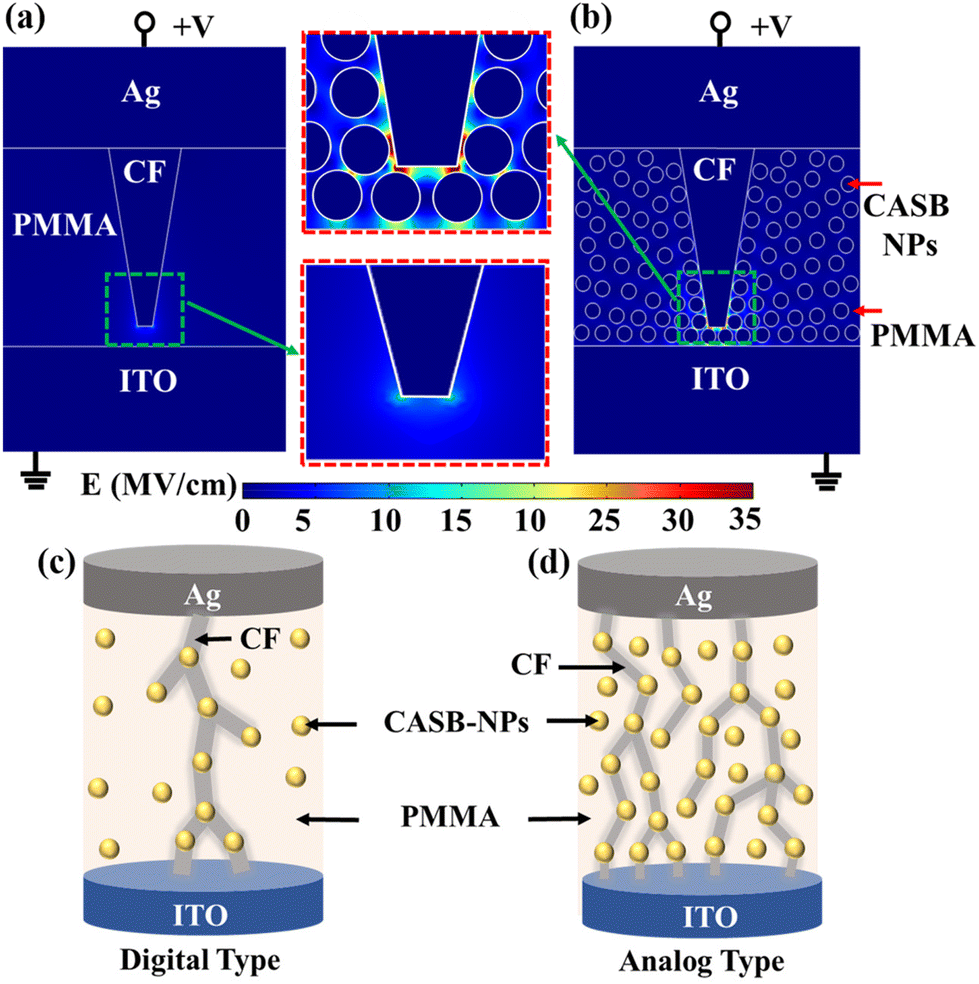 | ||
| Fig. 5 Simulated internal electric field in the memristor devices with different functional layers: (a) the PMMA layer without Cs2AgSbBr6-NPs and (b) the Cs2AgSbBr6-NPs homogeneously distributed in the PMMA layer. The local magnification of the electric field distributions is indicated. Schematic diagram of the RS behavior of (c) digital-type and (d) analog-type memristors. | ||
On the one hand, the enhanced electric field is relatively fixed in the location of Ag CFs growth, which reduces the randomness of CFs formation and rupture.12 Therefore, the addition of NPs significantly boosts the nucleation probability of Ag atoms in the switching layer, especially near the filament tips, promoting the growth of more CFs, which allows the device from being prematurely failed due to the insufficient number of growing CFs. It is inferred that this accounts for the improved RS performance of digital memristors (Fig. 5c). On the other hand, with the number of NPs continuing to grow, more CFs emerge along the location of the NPs. It is thought that the multiple weak CFs cause the conductance of the device to change continuously and slowly, making the memristors achieve digital-type to analog-type adjustable behavior (Fig. 5d).29 Table S1† compares the RS properties of several lead-free halide perovskite memristors. It can be observed that the prepared Cs2AgSbBr6-NPs memristors not only have lower operating voltage and cycling endurance, but most importantly, can modulate the local electric field in the switching layer and realize the transition from digital to analog type.
Conclusions
In conclusion, we have investigated the RS performance of the Ag/PMMA&Cs2AgSbBr6-NPs/ITO memristor devices with different concentrations of Cs2AgSbBr6-NPs. When the NPs doped in the PMMA film reach a concentration of about 5 wt%, the memristor devices demonstrated bipolar digital RS behaviors with excellent electrical characteristics such as low operating voltage, high ON/OFF ratio (>500), good endurance (>800 cycles), stable retention ability (>104 s), and more uniform switching voltages. Whereas, when the concentration of the NPs doped in the PMMA film is around 10 wt%, the memristors switch to continuously adjustable resistance states and several artificial synapse behaviors are successfully simulated. Moreover, the effect of NPs is explored through modeling the devices by simulation. It is suggested that the improved RS performance and the adjustable digital-to-analog conversion behavior are attributed to the local electric field and growing filaments affected by added NPs. Our study provides an approach to designing and fabricating the next-generation artificial synapse devices based on lead-free halide perovskites.Experimental
Materials
Cesium bromide (CsBr, 99.5%), silver bromide (AgBr, 99.9%), antimony bromide (SbBr3, 99%), oleylamine (OLAM, 80%–90%), isopropanol (IPA, analytical reagent), chlorobenzene (99.5%), oil acid (OA, 99%), and dimethyl sulfoxide (DMSO, analytical reagent) were purchased from Macklin Company. Poly(methyl methacrylate) (PMMA, analytical reagent) was purchased from Shanghai Aichun Biological Technology Co., Ltd. All reagents and solvents were used as received without any further purification.Synthesis of Cs2AgSbBr6 powders
Firstly, CsBr (0.213 g, 1.0 mmol), AgBr (0.094 g, 0.5 mmol), and SbBr3 (0.181 g, 0.5 mmol) were dissolved in 5 mL DMSO, 1 mL OA, and 0.15 mL OLAM in a water bath at 60 °C and stirred for 1 h. When the solution cooled to room temperature, 1 mL precursor solution was added into 10 mL isopropanol in a dropwise way and vigorous stirred for 1 min, forming a crude Cs2AgSbBr6-NPs solution. Subsequently, the crude solution was centrifuged at 9000 rpm for 5 min and the supernatant was discarded to obtain pure Cs2AgSbBr6-NPs. The solid powders were obtained by vacuum drying at 60 °C for 6 hours.Fabrication of PMMA&Cs2AgSbBr6-NPs based memristor
The patterned indium-tin-oxide (ITO) substrates (5 Ω sq−1) were ultrasonically cleaned in deionized water, acetone and ethanol for 20 min sequentially, and then treated with UV-zone for 5 min. In order to construct Ag/PMMA&Cs2AgSbBr6-NPs/ITO memristors with different mass fractions, the 90 mg PMMA powders were mixed with 0.91 mg, 2.78 mg, 4.74 mg, and 10 mg Cs2AgSbBr6 powders, respectively. After that, the mixed powders were dissolved in 6 mL of chlorobenzene and sonicated for 20 min to make a homogeneous solution. The solution was spin-coated on the ITO surface at 4000 rpm for 60 s, and annealed at 120 °C for 5 min. The above process was repeated for three times. Subsequently, the assembled PMMA&Cs2AgSbBr6-NPs films were formed after the final annealing at 120 °C for 20 min. Finally, the circular metal electrodes were deposited on the composite films using a shadow mask under vacuum evaporation to accomplish the fabrication.Characterizations
The X-ray diffraction (XRD) patterns were recorded at a scan speed of 2° min−1 by an X-ray diffractometer (Bruker AXS D8 Advance) with Cu Kα radiation. The transmission electron microscope (TEM) was investigated on JEOL JEM-F200. The top-view surface images and cross-sectional images were measured by a field-emission scanning electron microscope (Zeiss Sigma 300). A Shimadzu Spectrophotometer (UV-2600) was used to measure the absorption spectra of the Cs2AgSbBr6-NPs powders and transmission of the PMMA&Cs2AgSbBr6-NPs film. The electrical properties were measured at room temperature under air atmosphere by a semiconductor analyzer (Keysight B1505A).Author contributions
Y. Wang conceived and coordinated the project. N. Xu prepared the device and performed the electrical measurement. Y. Yuan and W. Zhang performed the measurements of XRD, SEM and the finite analysis. N. Xu, Y. Wang and Q. Huang wrote and commented on the manuscript. The study was supervised by X. Tang and F. Qi.Conflicts of interest
There are no conflicts to declare.Acknowledgements
This work was supported in part by the National Natural Science Foundation of China under Grant 61804020, the Natural Science Foundation Project of Chongqing under Grant cstc2019jcyj-msxmX0124, and the Scientific and Technological Research Foundation of Chongqing Municipal Education Commission under Grant (No. KJQN201800607, KJQN201900643, and KJQN202100611).References
- M. Janousch, G. I. Meijer, U. Staub, B. Delley, S. F. Karg and B. P. Andreasson, Adv. Mater., 2007, 19, 2232–2235 CrossRef CAS
.
- Y. Li, J. X. Chu, W. J. Duan, G. S. Cai, X. H. Fan, X. Z. Wang, G. Wang and Y. L. Pei, ACS Appl. Mater. Interfaces, 2018, 10, 24598–24606 CrossRef CAS PubMed
- C. H. Yang, J. Seidel, S. Y. Kim, P. B. Rossen, P. Yu, M. Gajek, Y. H. Chu, L. W. Martin, M. B. Holcomb, Q. He, P. Maksymovych, N. Balke, S. V. Kalinin, A. P. Baddorf, S. R. Basu, M. L. Scullin and R. Ramesh, Nat. Mater., 2009, 8, 485–493 CrossRef CAS PubMed
- K. J. Kwak, D. E. Lee, S. J. Kim and H. W. Jang, J. Phys. Chem. Lett., 2021, 12, 8999–9010 CrossRef CAS PubMed
- K. Kang, W. Hu and X. Tang, J. Phys. Chem. Lett., 2021, 12, 11673–11682 CrossRef CAS PubMed
- R. Waser, R. Dittmann, G. Staikov and K. Szot, Adv. Mater., 2009, 21, 2632–2663 CrossRef CAS PubMed
- Y. V. Pershin and M. Di Ventra, IEEE Trans. Circuits Syst. I: Regul. Pap., 2010, 57, 1857–1864 Search PubMed
- Y. Park and J.-S. Lee, ACS Nano, 2017, 11, 8962–8969 CrossRef CAS PubMed
- Y. P. Jiang, H. L. Zhou, X. G. Tang, Q. X. Liu, W. H. Li and Z. H. Tang, J. Asian Ceram. Soc., 2021, 9, 851–857 CrossRef
- X. Li, H. Wu, G. Bin, W. Wu, D. Wu, N. Deng, J. Cai and H. Qian, Nanotechnology, 2016, 27, 305201 CrossRef PubMed
- A. Saleem, F. M. Simanjuntak, S. Chandrasekaran, S. Rajasekaran, T.-Y. Tseng and T. Prodromakis, Appl. Phys. Lett., 2021, 118, 112103 CrossRef CAS
- L. Li, B. Liu, J. Feng, W. Hu, H. Lin, Y. Huang, D. Wu, F. Zeng, J. Zhou and X. Tang, Appl. Phys. Lett., 2021, 118, 222108 CrossRef CAS
- C. Liu, L. G. Wang, K. Qin, Y. Q. Cao, X. J. Zhang, D. Wu and A. D. Li, IEEE Trans. Electron Devices, 2018, 65, 4674–4678 CAS
- Y. Wang, H. Liu, X. Wang and L. Zhao, Nanoscale Res. Lett., 2019, 14, 224 CrossRef PubMed
- W. Banerjee, Electronics, 2020, 9, 1029 CrossRef CAS
- W. Banerjee, Q. Liu and H. Hwang, J. Appl. Phys., 2020, 127, 051101 CrossRef CAS
- Y. Wang, Y. Yuan, W. Zhang, F. Qi, N. Zhang, T. Liu and X. Tang, Appl. Phys. Lett., 2022, 120, 263503 CrossRef CAS
- Y. Wang, N. Xu, W. Zhang, Y. Yuan, F. Qi, N. Zhang and X. Tang, IEEE Trans. Electron Devices, 2022, 69, 6676–6680 CAS
- M. Lanza, H. S. P. Wong, E. Pop, D. Ielmini, D. Strukov, B. C. Regan, L. Larcher, M. A. Villena, J. J. Yang, L. Goux, A. Belmonte, Y. Yang, F. M. Puglisi, J. Kang, B. Magyari-Köpe, E. Yalon, A. Kenyon, M. Buckwell, A. Mehonic, A. Shluger, H. Li, T.-H. Hou, B. Hudec, D. Akinwande, R. Ge, S. Ambrogio, J. B. Roldan, E. Miranda, J. Suñe, K. L. Pey, X. Wu, N. Raghavan, E. Wu, W. D. Lu, G. Navarro, W. Zhang, H. Wu, R. Li, A. Holleitner, U. Wurstbauer, M. C. Lemme, M. Liu, S. Long, Q. Liu, H. Lv, A. Padovani, P. Pavan, I. Valov, X. Jing, T. Han, K. Zhu, S. Chen, F. Hui and Y. Shi, Adv. Electron. Mater., 2019, 5, 1800143 CrossRef
- J. Lao, W. Xu, C. Jiang, N. Zhong, B. Tian, H. Lin, C. Luo, J. Travas-sejdic, H. Peng and C.-G. Duan, J. Mater. Chem. C, 2021, 9, 5706–5712 RSC
- J. S. Han, Q. V. Le, J. Choi, H. Kim, S. G. Kim, K. Hong, C. W. Moon, T. L. Kim, S. Y. Kim and H. W. Jang, ACS Appl. Mater. Interfaces, 2019, 11, 8155–8163 CrossRef CAS PubMed
- Y. Wang, Z. Lv, Q. Liao, H. Shan, J. Chen, Y. Zhou, L. Zhou, X. Chen, V. A. L. Roy, Z. Wang, Z. Xu, Y.-J. Zeng and S.-T. Han, Adv. Mater., 2018, 30, 1800327 CrossRef PubMed
- H. S. P. Wong, H. Y. Lee, S. Yu, Y. S. Chen, Y. Wu, P. S. Chen, B. Lee, F. T. Chen and M. J. Tsai, Proc. IEEE, 2012, 100, 1951–1970 CAS
- S.-Y. Kim, J.-M. Yang, E.-S. Choi and N.-G. Park, Adv. Funct. Mater., 2020, 30, 2002653 CrossRef CAS
- H. Ye, B. Sun, Z. Wang, Z. Liu, X. Zhang, X. Tan, T. Shi, Z. Tang and G. Liao, J. Mater. Chem. C, 2020, 8, 14155–14163 RSC
- F. J. Zeng, Y. Y. Guo, W. Hu, Y. Q. Tan, X. M. Zhang, J. L. Feng and X. S. Tang, ACS Appl. Mater. Interfaces, 2020, 12, 23094–23101 CrossRef CAS PubMed
- Q. Wang, Y. Deng, J. Chen, L. Lu, Y. Ma and L. Zang, J. Alloys Compd., 2022, 927, 167117 CrossRef CAS
- W. Banerjee, S. H. Kim, S. Lee, D. Lee and H. Hwang, Adv. Electron. Mater., 2021, 7, 2100022 CrossRef CAS
- W. Wu, H. Wu, B. Gao, N. Deng, S. Yu and H. Qian, IEEE Electron Device Lett., 2017, 38, 1019–1022 CAS
Footnotes |
| † Electronic supplementary information (ESI) available. See DOI: https://doi.org/10.1039/d2nr06370k |
| ‡ These authors contributed equally to this paper. |
| This journal is © The Royal Society of Chemistry 2023 |