
 Open Access Article
 This Open Access Article is licensed under a
 Creative Commons Attribution 3.0 Unported Licence
Nanoarchitectonics in fully printed perovskite solar cells with carbon-based electrodes†
Dmitry
Bogachuk
 *a,
Jessica
Girard
b,
Siddharth
Tilala
a,
David
Martineau
b,
Stéphanie
Narbey
b,
Anand
Verma
b,
Andreas
Hinsch
a,
Markus
Kohlstädt
ac and
Lukas
Wagner
d
*a,
Jessica
Girard
b,
Siddharth
Tilala
a,
David
Martineau
b,
Stéphanie
Narbey
b,
Anand
Verma
b,
Andreas
Hinsch
a,
Markus
Kohlstädt
ac and
Lukas
Wagner
d
aFraunhofer Institute for Solar Energy Systems ISE, Heidenhofstr. 2, 79110 Freiburg, Germany. E-mail: dmitry.bogachuk@ise.fraunhofer.de
bSolaronix SA, Rue de l'Ouriette 129, Aubonne 1170, Switzerland
cFreiburg Materials Research Center FMF, University of Freiburg, Stefan-Meier-Str. 21, 79104 Freiburg, Germany
dSolar Energy Conversion Group, Department of Physics, Philipps-University Marburg, Renthof 7, 35037 Marburg, Germany
First published on 2nd January 2023
Abstract
A sacrificial film of polystyrene nanoparticles was utilized to introduce nano-cavities into mesoporous metal oxide layers. This enabled the growth of larger perovskite crystals inside the oxide scaffold with significantly suppressed non-radiative recombination and improved device performance. This work exemplifies potential applications of such nanoarchitectonic approaches in perovskite opto-electronic devices.
Perovskite solar cells (PSCs) have attracted the attention of numerous researchers over recent years due to the fascinating nature of these materials.1–3 After an unprecedentedly rapid increase in their reported power conversion efficiencies (PCEs), nowadays, more attention is being paid within the perovskite community to device stability.4 PSCs with carbon-based back-electrodes (CPSCs) are well-known to be highly stable under different ambient and operational conditions.5,6 However, their PCEs are still lower compared to state-of-the-art PSCs with metal-based electrodes.7
Mesoscopic CPSCs consist of a fluorine-doped tin oxide (FTO) front electrode, compact titanium dioxide (c-TiO2), mesoporous titanium dioxide (m-TiO2), zirconium dioxide (ZrO2) and a carbon back-electrode. The carbon electrode is usually treated at high temperatures, meaning that perovskite can only be introduced after the back-electrode is deposited. Consequently, the entire device structure must be porous, to allow the solution to fill the scaffold and to consequently crystallize the perovskite within this porous matrix between the front and the back electrode. Therefore, the perovskite crystal size and density of grain boundaries (GBs) are determined by the pore size, because they confine the perovskite growth. Since the particles of m-TiO2, ZrO2 layers and corresponding pores are typically 20 nm in diameter or less,8,9 the perovskite grown within these layers is expected to have numerous GBs with surface defect states. As has been shown in our earlier study,10 this causes substantial non-radiative recombination and limits their potential to reach the highest open-circuit voltage (VOC).
Consequently, to overcome this limitation, one needs to enlarge the perovskite crystal size. This implies that the pores in which the perovskite is formed need to be enlarged in order to grow crystals with fewer GBs. In a CPSC stack there are three porous layers: m-TiO2, ZrO2 and carbon – all of which are filled with perovskite. The m-TiO2 layer should be thin to minimize parasitic absorption and interfacial non-radiative recombination losses9 and porous enough to avoid capacitance issues,11 which arise from the high dielectric constant of TiO2.12 As a result, PSCs with TiO2 having a small surface area (e.g. those having only planar TiO2) typically have severe hysteresis of the JV-characteristics.1,4 This limits the possibility of tuning the well-optimized pore size of the m-TiO2 layer. The porosity of the carbon layer affects the solution permeability13 and the electrode series resistance14 but not the non-radiative recombination since the perovskite embedded in this layer is essentially “in the dark” (i.e. far beyond the optical generation profile9). In contrast, enlarging the pores of ZrO2 is still a rather unexplored option and will likely suppress the non-radiative recombination rate of the perovskite within due to the reduced density of GBs and have the most prominent effect on the device performance.10
In this work, we propose the use of nanoarchitectonics – utilization of nano-scaled and well-arranged structural units – to modify the architecture of an opto-electronic device, in this case a CPSC. By utilizing inkjet-printed polystyrene (PS) nanoparticles as a sacrificial template between m-TiO2 and ZrO2 layers, we were able to facilitate the formation of cavities at this interface, which will be filled with large perovskite crystals after cell manufacturing is complete. The developed inkjet-printing process allows one to deposit highly ordered layers of hexagonally arranged PS nanoparticles, on which the ZrO2 layer could be flawlessly deposited. During ZrO2 sintering, the PS nanoparticles pyrolyze, acting as a sacrificial template to nanostructure the ZrO2 layer. A 3D-nanotomogramm of the sample obtained via scanning electron microscopy coupled with focused ion-beam ablation (SEM-FIB) confirmed the successful alternation of the device structure and the introduction of the enlarged cavity. Furthermore, steady-state and transient PL measurements clearly show that perovskite-filled scaffolds with such a cavity exhibit reduced non-radiative recombination, slightly boosting the charge-carrier lifetime and device VOC. The nano-architectured CPSCs also exhibited a slightly better ideality factor and reduced non-radiative fill factor (FF) losses coming from the higher pseudo-fill factor. Furthermore, the nano-architectured cells exhibit a small improvement in short-circuit current density (JSC) by approximately 1.5 mA cm−2 suggesting an increase in light absorption due to a slightly higher photoabsorber volume. Overall, the best nano-architectured cell had an impressive PCE of 15.7%. Although this study is focused particularly on improving the performance of CPSCs with such techniques, the concept of nanoarchitectonics could be explored in other PSC architectures as well and provides immense potential for further device enhancement.
Firstly, to deposit a film of PS nanoparticles, a PS suspension was diluted with methanol and spin-coated on the FTO. After drying the film, its morphology was investigated using a scanning electron microscope (SEM). We note that to improve the layer packing density, surfactant Triton X-100 was added, allowing for the deposition of a compact and homogeneous film (Fig. S1a†). However, to be used in an up-scalable inkjet-printing process (Fig. 1), the diluted suspension needed to be optimized further. In order to avoid clogging of the head nozzles, methanol was replaced with isopropanol, and the resulting suspension was further diluted with 1-pentanol. Furthermore, we used formamide to induce better Marangoni flows, which counteract the convective flows, thus minimizing the droplet diameter and avoiding the “coffee-ring effect”.15 With this optimized PS suspension, a well-ordered arrangement of PS nanoparticles was obtained. Surprisingly, the PS particles in the inkjet-printed layers are hexagonally arranged and appear to be even more ordered than in the case of spin-coated films (Fig. S1b†). However, the spin-coated films were slightly thicker than the printed ones (Fig. S1c and d†), which could be related to the difference in the ink composition. For further experiments, we only utilized the inkjet-printing technique to coat the substrate with PS nanoparticles.
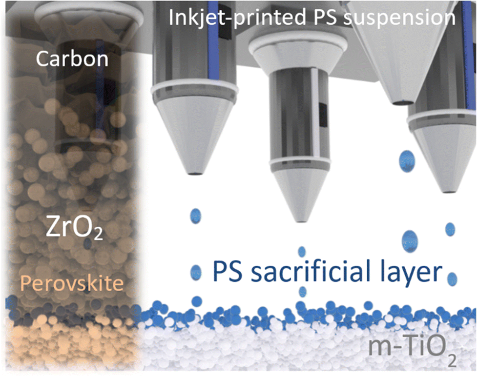 | ||
| Fig. 1 Conceptual illustration depicting an inkjet-printing process of a sacrificial layer of polystyrene (PS) particles for nano-architectured perovskite solar cells with carbon-based electrodes with a solar cell structure depicted on the left. | ||
ZrO2 was then screen-printed on top of the deposited PS layer followed by a slow sintering process (heating up to 500 °C), which is similar to other nanoarchitectonic approaches to structure the photoabsorber in PSCs.16 Such a method resulted in the formation of localized nano-cavities between the FTO and the ZrO2 layers, without delamination of the latter layer from the substrate (Fig. 2a). For a more visual comparison, Fig. 2b shows that the reference sample with ZrO2 deposited on the FTO substrate does not display such a feature. However, the cavity height is significantly lower than the thickness of the initially deposited PS layer. During ZrO2 sintering the PS particles undergo the transition from the solid state to rubbery and viscous states, followed by their depolymerization and evaporation. Therefore, most likely the height of the PS layer shrinks during the transition to the rubbery state.
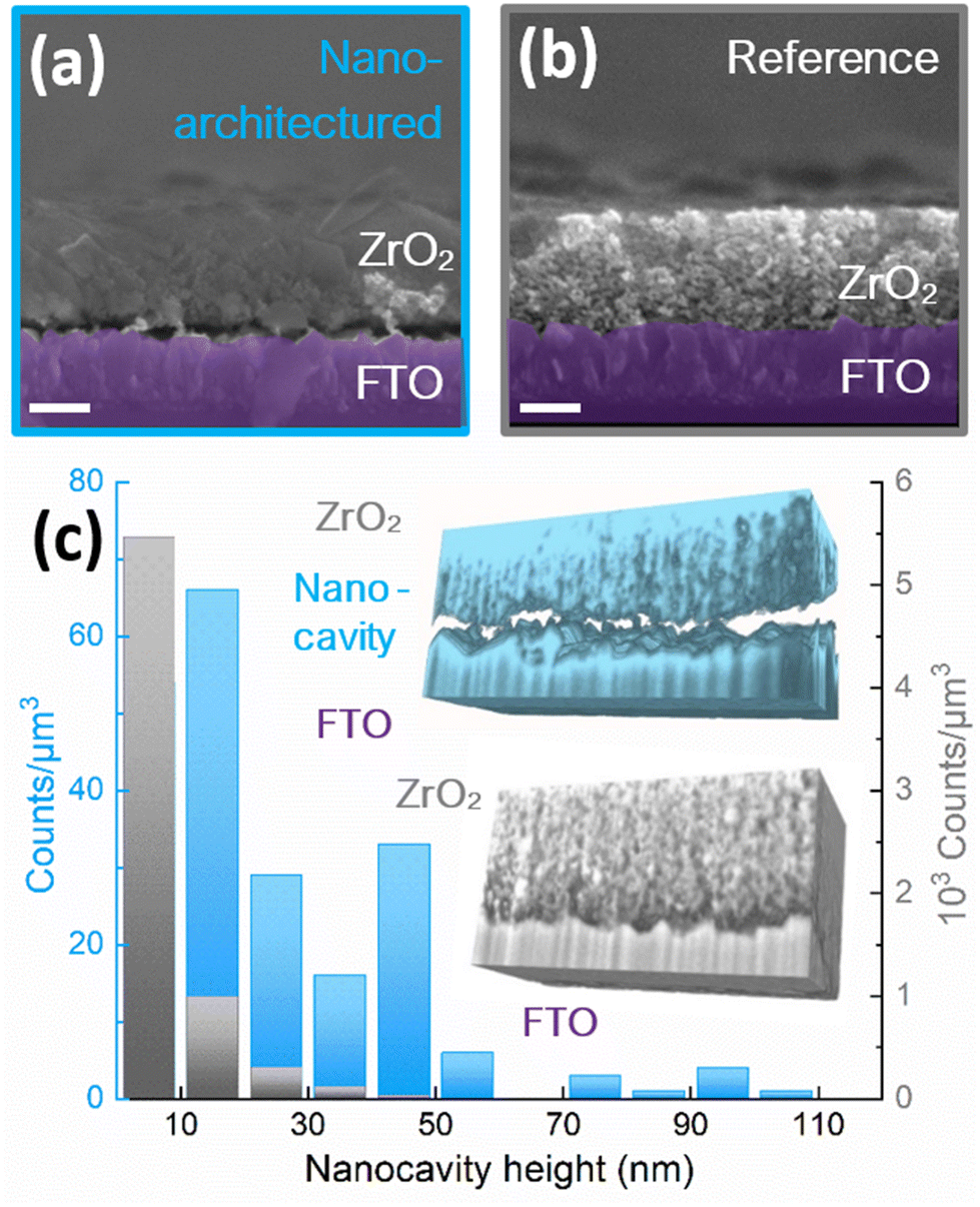 | ||
| Fig. 2 Cross-sectional scanning electron microscopy (SEM) images of (a) the nano-architectured layer of ZrO2 and (b) the reference layer of ZrO2. Scale bars – 500 nm. (c) Distribution of the cavity height in the nano-architectured (blue) and reference (grey) samples, obtained from 3D-nanotomography using focused ion-beam (FIB) ablation. | ||
To quantify the nano-cavity height distribution in a sample we utilize FIB-SEM tomography, whereby we successively polish the cross-section and record the SEM images of the polished surface allowing one to obtain information about the sample's appearance along its depth. Combining these 2D SEM images along the axis perpendicular to the plane of the recorded images allows us to reconstruct a 3D image of our nanoengineered structure and compare it with the reference one (Fig. 2c). Then the 3D-nanotomogramms were analyzed (via image analysis software ImageJ) to plot a distribution of the nano-cavity height with the polished ∼2 μm3 sample volume. The distribution in Fig. 2c revealed that additional localized cavities up to 100 nm in height have been introduced overall across the sample. In comparison, the 3D-nanotomogramm and the corresponding distribution of a reference sample demonstrate that it does not possess such a feature with most cavities being below 10 nm which is likely to originate from the porosity of ZrO2.
Next, we filled the nano-architectured samples with a perovskite to study the effect of large perovskite grains grown within ZrO2 on the radiative and non-radiative recombination rates. The mixed-dimensional 2D/3D perovskite photoabsorber layer was primarily composed of methylammonium lead iodide (MAPbI3) with a small addition of 5-aminovaleric acid (5-AVA) similar to our previous works.6,10,14 As can be seen from the TRPL measurement shown in Fig. 3a, the effective decay time constant (τ) of the PS samples was found to be 760 ns by fitting the PL behavior to a bi-exponential decay. This is significantly higher than that in the case of the perovskite embedded in the reference ZrO2 layer, which was found to be 570 ns. A higher τ in the nano-architectured samples suggests a prolonged charge-carrier lifetime resulting from the effective suppression of non-radiative recombination via reduction of grain boundaries in the perovskite.
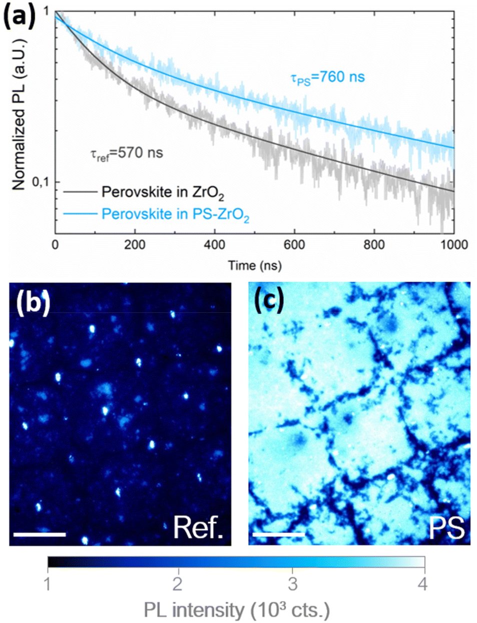 | ||
| Fig. 3 (a) Time-resolved photoluminescence (TRPL) measurements of the perovskite embedded in reference ZrO2 and nano-architectured ZrO2 (PS-ZrO2), showing a difference in the decay constant and charge-carrier lifetime. Steady-state PL maps of (b) reference perovskite solar cells with carbon electrodes and (c) nano-architectured cells with a PS sacrificial layer. Scale bar – 150 μm. | ||
To test whether this nano-architecturing approach also results in an improvement of PV devices, we manufactured CPSCs with and without the nano-cavity. The m-TiO2, ZrO2 and carbon-based layers constituting the cell stack (as shown in Fig. 1) had thicknesses of 0.4, 1 and 12 μm, respectively. In accordance with the prolongation of PL decay and charge-carrier lifetime, the PL mapping in Fig. 3b reveals that the reference CPSCs have a much lower PL intensity than the PS samples (Fig. 3c). Note that the square patterns in both PL maps originate from the mesh of the screen-printing stencil (during deposition of TiO2) and are not related to the PS layer. Therefore, a high PL intensity and a long charge-carrier lifetime indicate that the non-radiative recombination in such cells is reduced, which would positively affect device performance.
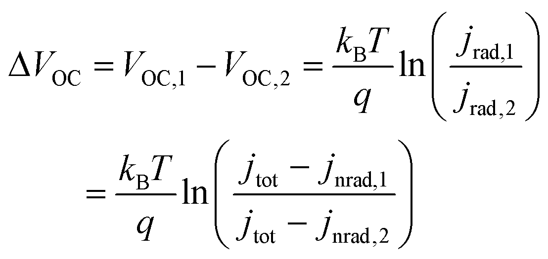
The measured statistical data obtained from the current–voltage measurements of the manufactured cells are presented in Fig. 4a, demonstrating that the nanostructured samples cause a significant enhancement in VOC by approximately 30–40 mV and in JSC by ∼1.5 mA cm−2. We attribute the improvement in JSC to better light absorption and less scattering by ZrO2 particles, which slightly increases the incident photon-to-electron conversion efficiency (IPCE) as seen from Fig. S2.† The electrochemical impedance spectroscopy (EIS) measurements in Fig. S3† show that the charge-transfer resistance is reduced in the nano-architectured CPSCs, while the ohmic series resistance is unchanged leading to only a marginal improvement in the FF. Previously, we have also reported a similar decrease in the charge-transfer resistance, when a 2D perovskite layer was used to suppress non-radiative recombination and improve hole extraction.17 To study the enhancement of VOC, we utilize the following equation derived from the Ross relation18 (detailed derivation can be found in ESI note 1†), showing that the difference in VOC directly depends on the ratio of the PLQY and jnradvia:
 | (1) |
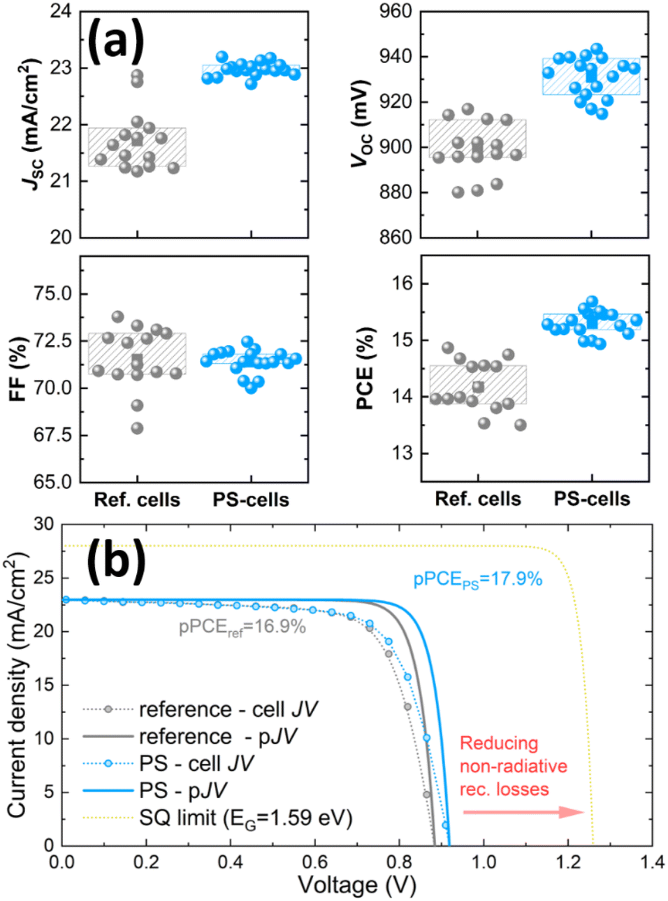 | ||
| Fig. 4 (a) Short-circuit current density (JSC), open-circuit voltage (VOC), fill factor (FF) and power conversion efficiencies of manufactured CPSCs with and without a sacrificial PS layer. (b) JV curves and pseudo-JV curves of the optimum reference and nano-architectured cells, in comparison with the curve at the Shockley–Queisser limit. | ||
Considering that the mean difference in VOC between the reference and the nano-architectured cells is ∼33 mV, the jrad and PLQY values should increase by 3.5 times, which agrees remarkably well with the intensity difference of the PL maps shown in Fig. 3b and c. We have also simulated CPSCs with different grain sizes using a 1D drift-diffusion model similar to our previous work10 to demonstrate an increase in the quasi-Fermi level splitting (QFLS) and implied VOC due to the grain size increase (Fig. S4†). Notably, the grain size starts to play a particularly important role in cells with a large grain boundary density due to the logarithmic dependency of the QFLS, and the measured increase in VOC by 33 mV would correspond to the doubling of the grain size from 25 to 50 nm (30.5 mV according to the simulated results).
To further investigate the reduction of non-radiative recombination losses we measured the light intensity-dependent VOC value to extract the ideality factor n. The slightly lower ideality factor (as shown in Fig. S5†) confirms that the non-radiative recombination losses are suppressed in the CPSCs with nano-cavities. Considering that no foreign materials have been introduced (for passivation, better charge selection, energy alignment etc.) and the only change is the presence of larger pores, we attribute the decrease in non-radiative recombination to the growth of larger perovskite crystals.
From the JV-statistics in Fig. 4a we also highlight an exceptional reproducibility of this approach with a standard deviation of the PCE of only 0.2%, in comparison with the standard deviation of 0.5% in the case of reference cells. Furthermore, the best PS-engineered cell showed a VOC value of 940 mV and a PCE value of 15.7% (Fig. S6†).
Next, we used the light intensity-dependent behavior of VOC–JSC pairs to construct a so-called pseudo-JV curve (pJV curve). Since VOC is measured under an open circuit, the charge transport outside of the cell is absent and therefore the effect of series resistance can be neglected. Thus, the pJV curve represents a JV curve of a cell in the absence of charge-transport losses, which is then only limited by non-radiative recombination losses.17,19,20Fig. 4b shows the JV and pJV curves of the reference and nano-architectured CPSCs based on the measurements in Fig. S5.† These indicate that by minimizing the series resistance losses, the nano-architectured CPSC could reach a potential PCE (pPCE) of nearly 18%. In addition, Fig. 4b shows a JV curve of an “ideal” solar cell with this perovskite bandgap (1.59 eV according to the Tauc plot in Fig S7),14 where only the radiative recombination is present, according to the Shockley–Queisser limit. By comparing the measured JV curves with an ideal one, we see that the biggest PCE loss is due to the VOC, which is reduced by nearly 320 mV. This substantial gap implies that although the presented approach can suppress the non-radiative recombination at the GBs to some extent, there is still a lot of room for further improvement.
In summary, we demonstrated an effective strategy to engineer the architecture of perovskite solar cells with carbon-based electrodes in order to create nano-cavities between the m-TiO2 and the ZrO2 layers. These nano-cavities were formed by depositing ZrO2 on an inkjet-printed and highly ordered layer of polystyrene nanoparticles, which acts as a sacrificial template to foster the controlled formation of a nano-cavity. The success of this approach was confirmed by SEM observations coupled with cross-sectional FIB polishing to produce a 3D-nanotomogramm of the nano-architectured sample, from which we quantified the cavity height distribution by image analysis. Even though the cavity height (and therefore the maximum perovskite crystal height) is <100 nm, we demonstrate by transient and steady-state PL-mapping measurements that these nano-cavities still cause a suppression of non-radiative recombination in the perovskite photoabsorber and lead to an improvement in the charge-carrier lifetime. Consequently, the VOC value has been improved by nearly 40 mV, which is accompanied by a small increase in JSC, resulting in a remarkable PCE of 15.7%. Furthermore, by performing light intensity-dependent measurements, we show that the ideality factor n has been reduced in cells with larger perovskite crystals, agreeing with the results from PL analysis. Based on these measurements, we construct a pseudo-JV curve, demonstrating the potential of these nano-architectured cells to reach a PCE of 17.9%, if the charge-transport losses could be minimized. The findings of this work provide a conceptually new idea of utilizing nanoarchitectonics in PSCs as a new method to boost their PV performance (particularly in the case of devices with mesoporous structures), and potentially bring it closer to the radiative limit.
Conflicts of interest
There are no conflicts to declare.Acknowledgements
This work was funded by project UNIQUE supported under the umbrella of a SOLAR-ERA.NET_cofund by ANR, PtJ, MIUR, MINECO-AEI and SWEA, within the EU's HORIZON 2020 Research and Innovation Program (cofund ERA-NET Action no. 691664) DOI: 10.3030/101084124 and by European Union's Horizon Europe Framework Programme for research and innovation under grant agreement no. 101084124 (DIAMOND). D.B. also acknowledges support from the German Federal Environmental Foundation (DBU).References
- J. Y. Kim, J.-W. Lee, H. S. Jung, H. Shin and N.-G. Park, Chem. Rev., 2020, 120, 7867–7918 CrossRef CAS PubMed
.
- J.-P. Correa-Baena, M. Saliba, T. Buonassisi, M. Grätzel, A. Abate, W. Tress and A. Hagfeldt, Science, 2017, 358, 739–744 CrossRef CAS PubMed
- Y. Rong, Y. Hu, A. Mei, H. Tan, M. I. Saidaminov, S. I. Seok, M. D. McGehee, E. H. Sargent and H. Han, Science, 2018, 361, 1214 CrossRef CAS PubMed
- Q. Wang, N. Phung, D. Di Girolamo, P. Vivo and A. Abate, Energy Environ. Sci., 2019, 12, 865–886 RSC
- A. Mei, Y. Sheng, Y. Ming, Y. Hu, Y. Rong, W. Zhang, S. Luo, G. Na, C. Tian, X. Hou, Y. Xiong, Z. Zhang, S. Liu, S. Uchida, T.-W. Kim, Y. Yuan, L. Zhang, Y. Zhou and H. Han, Joule, 2020, 4, 2646–2660 CrossRef CAS
- D. Bogachuk, K. Saddedine, D. Martineau, S. Narbey, A. Verma, P. Gebhardt, J. P. Herterich, N. Glissmann, S. Zouhair, J. Markert, I. E. Gould, M. D. McGehee, U. Würfel, A. Hinsch and L. Wagner, Sol. RRL, 2022, 6, 2100527 CrossRef CAS
- D. Bogachuk, S. Zouhair, K. Wojciechowski, B. Yang, V. Babu, L. Wagner, B. Xu, J. Lim, S. Mastroianni, H. Pettersson, A. Hagfeldt and A. Hinsch, Energy Environ. Sci., 2020, 13, 3880–3916 RSC
- L. Wagner, C. Qiu, M. Unmüssig, D. Bogachuk, S. Mastroianni, U. Würfel, Y. Hu, H. Han and A. Hinsch, Sol. RRL, 2021, 5, 2000595 CrossRef CAS
- T. Liu, Y. Rong, Y. Xiong, A. Mei, Y. Hu, Y. Sheng, P. Jiang, X. Hou, M. Duan, Y. Guan, L. Hong and H. Han, RSC Adv., 2017, 7, 10118–10123 RSC
- D. Bogachuk, B. Yang, J. Suo, D. Martineau, A. Verma, S. Narbey, M. Anaya, K. Frohna, T. Doherty, D. Müller, J. P. Herterich, S. Zouhair, A. Hagfeldt, S. D. Stranks, U. Würfel, A. Hinsch and L. Wagner, Adv. Energy Mater., 2022, 12, 2103128 CrossRef CAS
- H.-S. Kim, I.-H. Jang, N. Ahn, M. Choi, A. Guerrero, J. Bisquert and N.-G. Park, J. Phys. Chem. Lett., 2015, 6, 4633–4639 CrossRef CAS PubMed
- J. Y. Kim, H. S. Jung, J. H. No, J.-R. Kim and K. S. Hong, J. Electroceram., 2006, 16, 447–451 CrossRef CAS
- R. Tsuji, D. Bogachuk, D. Martineau, L. Wagner, E. Kobayashi, R. Funayama, Y. Matsuo, S. Mastroianni, A. Hinsch and S. Ito, Photonics, 2020, 7, 133 CrossRef CAS
- D. Bogachuk, R. Tsuji, D. Martineau, S. Narbey, J. P. Herterich, L. Wagner, K. Suginuma, S. Ito and A. Hinsch, Carbon, 2021, 178, 10–18 CrossRef CAS
- E. Sowade, T. Blaudeck and R. R. Baumann, Nanoscale Res. Lett., 2015, 10, 362 CrossRef PubMed
- M. T. Hörantner, W. Zhang, M. Saliba, K. Wojciechowski and H. J. Snaith, Energy Environ. Sci., 2015, 8, 2041–2047 RSC
- S. Zouhair, S.-M. Yoo, D. Bogachuk, J. P. Herterich, J. Lim, H. Kanda, B. Son, H. J. Yun, U. Würfel, A. Chahboun, M. K. Nazeeruddin, A. Hinsch, L. Wagner and H. Kim, Adv. Energy Mater., 2022, 12, 2200837 CrossRef CAS
- R. T. Ross, J. Chem. Phys., 1967, 46, 4590–4593 CrossRef CAS
- S. Zouhair, B. Luo, D. Bogachuk, D. Martineau, L. Wagner, A. Chahboun, S. W. Glunz and A. Hinsch, Sol. RRL, 2022, 6, 2100745 CrossRef CAS
- B. Yang, J. Suo, F. Di Giacomo, S. Olthof, D. Bogachuk, Y. Kim, X. Sun, L. Wagner, F. Fu, S. M. Zakeeruddin, A. Hinsch, M. Grätzel, A. Di Carlo and A. Hagfeldt, ACS Energy Lett., 2021, 6, 3916–3923 CrossRef CAS PubMed
Footnote |
| † Electronic supplementary information (ESI) available. See DOI: https://doi.org/10.1039/d2nr05856a |
| This journal is © The Royal Society of Chemistry 2023 |