
Correlation between hysteresis dynamics and inductance in hybrid perovskite solar cells: studying the dependency on ETL/perovskite interfaces†
Rana
Yekani
a,
Hsien-chieh
Chiu
a,
Dallas
Strandell
 b,
Zhuoran
Wang
c,
Stéphanie
Bessette
a,
Raynald
Gauvin
a,
Patanjali
Kambhampati
b and
George P.
Demopoulos
*a
b,
Zhuoran
Wang
c,
Stéphanie
Bessette
a,
Raynald
Gauvin
a,
Patanjali
Kambhampati
b and
George P.
Demopoulos
*a
aMaterials Engineering Department, McGill University, 3610 University Street, H3A 0C5 Montreal, Canada. E-mail: george.demopoulos@mcgill.ca
bDepartment of Chemistry, McGill University, 801 Sherbrooke Street, H3A 0B8 Montreal, Canada
cICFO – The Institute of Photonic Sciences, Avinguda Carl Friedrich Gauss, 3, 08860 Castelldefels, Spain
First published on 30th December 2022
Abstract
In this study, to elucidate the origin of inductance and its relationship with the phenomenon of hysteresis in hybrid perovskite solar cells (PSCs), two electron transport layer (ETL) structures have been utilized: (a) rutile titania nanorods grown over anatase titania (AR) and (b) anatase titania covering the rutile titania nanorods (RA). The rutile and anatase phases are prepared via hydrothermal synthesis and spray pyrolysis, respectively. PSCs based on an ETL with an RA structure attain higher short-circuit current density (JSC) and open-circuit voltage (VOC) while showing a slightly lower fill factor (FF) compared with their AR counterparts. Using electrochemical impedance spectroscopy (EIS) measurements, we show that the ETL plays a major role in setting the tone for ionic migration speed and consequent accumulation. Moreover, we consider the conductivity of transport layers as a determining factor in not only giving rise to inductive features but also dictating the bias region under which recombination takes place, ultimately influencing hysteresis locus.
Introduction
Since their initial breakthrough in 2009, hybrid organic–inorganic perovskite solar cells (PSCs) have come a long way from a mere 3.9% power conversion efficiency (PCE)1 to over 25% in 2021.2 After only a decade, PSCs have shown considerable potential to compete with silicon solar cells.3 In PSCs, the absorber possesses an ABX3 perovskite structure where A is a monovalent cation, B is a divalent cation and X is a halide. Because they exhibit phenomenal properties such as long electron–hole diffusion length,4 high absorption coefficient,5 low exciton binding energies6 and defect tolerance,7 PSCs have been receiving unparalleled research attention over the past decade. Unlocking their full potential, however, relies on overcoming major challenges such as hysteresis.Hysteresis is the term applied to the mismatch between current–voltage (J–V) curves during reverse and forward scans.8 The major culprit, as reported in the literature, is the ionic charge redistribution within perovskite films as a response to external stimuli,9,10 coupled with non-radiative recombination at interfaces. Over the past decade, there has been a considerable improvement regarding devising various perovskite engineering and chemistry approaches for minimizing hysteretic occurrences.11,12 Electron transport layers (ETLs) and hole transport layers (HTLs) are known to exert a heavy influence on hysteresis through their defect properties,13,14 passivation,15 chemistry16 and utilization in various architectures.17
A probing method that has been commonly utilized to characterize PSCs, especially at the interfaces, and identify hysteretic features is electrochemical impedance spectroscopy (EIS).18 Yet, the interpretation of the resulting spectra has proved to be difficult and is drawing intense debate in some cases. One example is the origin and implication of lower frequency capacitance under illumination. An early round of studies attributed this feature to accumulation of electronic charge at the interfaces.19,20 A subset of lower frequency capacitance is called inductance (otherwise known as negative capacitance)21–24 which appears as a hook or a loop in the Nyquist plot representation of EIS measurements and is believed to be detrimental to PSC performance.25 Inductance has been interpreted in various ways in the literature such as the emptying rate of an intermediate state19 and interfacial charge transfer resistance.26 Recently, it has been shown27–30 that the capacitance element in lower frequency is rather due to the phase difference between the applied voltage and recorded current density, yet, its response is manifested similar to that of a physical inductor. Note that in this interpretation, the role of electrode polarization is not completely disregarded but it is believed to make a minor contribution towards the observed capacitance response. Based on this definition, inductance is mainly attributed to ionic modulation of the potential barrier at perovskite interfaces and the subsequent injection current from the contacts.30
Apart from the observation of inductance in PSCs with normal planar,19 mesoporous27 and even ETL-free architectures,31 other works32 have deliberately utilized multi-layered ETL structures to boost the number of charge injection processes involved in inducing the appearance of inductance in EIS spectra. In this work, to acquire a deeper understanding of the hysteresis phenomenon and its correlation with inductance, PSCs with two different titania ETL structures (that differ in their crystallographic phase and sequence of deposition) are studied. The variation in the ETL phase composition and structure is achieved by using spray pyrolysis (to deposit the anatase phase film) and hydrothermal synthesis (for obtaining the rutile phase in the nanorod morphology). The two phases are then stacked alternately in FTO/anatase/rutile and FTO/rutile/anatase architectures to yield AR and RA structures, respectively. The ETLs are characterized through a combination of techniques such as scanning electron microscopy (SEM), X-ray diffraction (XRD), cyclic voltammetry, atomic force microscopy (AFM), ultraviolet-visible (UV-vis) absorption, photoluminescence (PL), time-resolved photoluminescence (TRPL) and EIS. Utilizing the mentioned ETL architectures allows us to build a theory for interpreting the inductance features appearing in the mild and lower frequency parts of Nyquist plot and correlating them with hysteresis dynamics in PSCs.
The obtained results demonstrate that under fixed parameters corresponding to the synthesis and deposition of the perovskite layer and the HTL, the locus of hysteresis is dictated by the ETL. Moreover, the bias range in which the hysteresis locus appears is indicative of the corresponding electronic band structure. We postulate that the inductive hook at low frequency is a manifestation of non-radiative recombination under inverted bands at the ETL/perovskite interface.
Experimental section
Synthesis of the ETLs
For all ETL-related synthesis purposes, the FTO glass substrates (2 cm by 2 cm in dimension and pre-patterned) were purchased from Solaronix (with a surface resistivity of 7 Ohm per square and a thickness of 2.2 mm; part number: TCO22-7/LI). The substrates were ultrasonically cleaned sequentially in a 2% Hellmanex solution in DI water, 2-propanol, and acetone, for 15 min in each solvent. Eventually, the substrates were treated for 15 min with UV-ozone.The growth of the rutile nanorod film was carried out using hydrothermal synthesis.33 The reaction solution was made with 0.02 L of DI water and 0.02 L of concentrated hydrochloric acid (36.5%–38% by weight from Fisher Scientific). The mixture was stirred at room temperature in a sealed beaker for 5 minutes before the addition of 0.001 L of Ti(IV) butoxide (Reagent grade 97%, Sigma Aldrich). After stirring for another 40 min, the precursor solution was added to a Teflon-lined stainless-steel autoclave (0.125 L volume, Parr Instrument Co.), where the two substrates were placed at an angle with their conductive sides facing the wall. The autoclave was then sealed, placed in the oven and heated with a heating rate of 10 °C per hour to reach the final temperature of 150 °C where they were held for 60 minutes before cooling down inside the oven, which took approximately 3 hours. After the synthesis was performed, the substrates were taken out and washed thoroughly with DI water. Afterwards, they underwent an annealing step at a heating rate of 4 °C min−1 to 550 °C with a holding time of 30 minutes before cooling down.
The anatase phase was synthesized using spray pyrolysis. Cleaned FTO substrates were placed on a hot plate and heated gradually to 450 °C. Then a precursor solution containing 9 mL of ethanol, 0.6 mL of Ti(IV) diisopropoxide bis-acetylacetonate (Sigma Aldrich) and 0.4 mL of acetylacetone (Sigma Aldrich) was sprayed over the samples using O2 as a carrier gas.
Synthesis of the perovskite layer and HTL
The perovskite layer is synthesized and deposited according to the procedure described by Saliba et al.34 In short, the perovskite precursor was prepared by mixing FAI (1 M), PbI2 (1.1 M), MABr (0.2 M) and PbBr2 (0.2 M) in DMF/DMSO (4![[thin space (1/6-em)]](https://www.rsc.org/images/entities/char_2009.gif) :1 v/v). CsI (1.5 M in DMSO) and RbI (1.5 M in DMF:DMSO 4:1 v/v) were added to the perovskite precursor to obtain the quadruple cation composition of (Cs5Rb5MA0.15FA0.75)Pb(I0.83Br0.17)3. The perovskite layer is deposited by the anti-solvent method using 150 μL of the final perovskite precursor and using a two-step spinning program: 1000 rpm for 10 seconds followed by 6000 rpm for 20 seconds. Five seconds before the end of spinning, 200 μL of chlorobenzene was poured on the spinning substrate. The substrates were then annealed at 100 °C for 45 minutes. Except for PbI2 and PbBr2 which were sourced from TCI America, all other chemicals were purchased from Sigma Aldrich.
:1 v/v). CsI (1.5 M in DMSO) and RbI (1.5 M in DMF:DMSO 4:1 v/v) were added to the perovskite precursor to obtain the quadruple cation composition of (Cs5Rb5MA0.15FA0.75)Pb(I0.83Br0.17)3. The perovskite layer is deposited by the anti-solvent method using 150 μL of the final perovskite precursor and using a two-step spinning program: 1000 rpm for 10 seconds followed by 6000 rpm for 20 seconds. Five seconds before the end of spinning, 200 μL of chlorobenzene was poured on the spinning substrate. The substrates were then annealed at 100 °C for 45 minutes. Except for PbI2 and PbBr2 which were sourced from TCI America, all other chemicals were purchased from Sigma Aldrich.
Spiro-OMeTAD was chosen as the HTL material. The precursor solution was made from 72.3 mg of spiro-OMeTAD, 28.3 μL of 4-TBP and 17.5 μL of LiTFSI (520 mg mL−1 in acetonitrile) in 1 mL of chlorobenzene. Deposition of the HTL was conducted by spin casting 30 μL of the precursor solution at 3000 rpm. To dope the spiro-OMeTAD film, the samples were left in dry air under darkness overnight. Finally, 80 nm of gold was thermally evaporated (NexDep, Angstrom Engineering) under 2 × 10⁻⁶ mbar vacuum at a rate of 1 A s−1.
J–V and EIS measurements
The illumination measurements were conducted with a class A solar simulator (Sol1A 94021A, Newport) which was calibrated with a silicon KG5 reference cell (Abet Technologies). To measure the PV metrics, the J–V curves were recorded under 1 sun at 100 and 10 mV s−1 from −0.2 V (vs. reference electrode) to 0.2 V above VOC. All EIS measurements were conducted under 1 sun illumination and various forward bias values with a Biologic potentiostat (SP-300) and controlled using the EC lab software from 1 MHz to 50 MHz, with a perturbation potential of 20 mV over 40 data points. There was a total of four devices on each sample, with an active area of 0.09 cm2. The illumination intensity for all J–V and EIS measurements was 1 sun.X-Ray diffraction (XRD)
The XRD patterns were acquired using a Bruker D8 Advance. A copper source (Kα line) was used with a voltage of 40 kV and a current of 40 mA. Scan parameters were 2 theta values from 6° to 70° with an increment of 0.02° and an integration time of 1 s. The experiment was performed in the grazing incidence diffraction mode with a low incident angle of 3°. Both the primary and secondary axial Soller was 2.5° while the secondary twin optic was set to Soller 0.2°. The LynxEye detector was set to 0D mode.Cyclic voltammetry measurements
Cyclic voltammetry measurements were carried out in a one-compartment cell using a Biologic potentiostat (SP-300) and controlled using the EC lab software. Ag/AgCl (sat. KCl) and Au were used as the reference and counter electrodes, respectively. The electrolyte was 0.5 mM K4Fe(CN)6 (Sigma Aldrich) + 0.5 mM K3Fe(CN)6 (Sigma Aldrich) in aqueous 0.5 M KCl (Sigma Aldrich). The voltage was scanned from −1 V to 1 V at a rate of 25 mV s−1. The effective electrode area was 1 cm2.Scanning electron microscopy (SEM)
The cross sectional and top view SEM images were obtained with a cold-field emission scanning electron microscope (CFE-SEM) SU8230 Hitachi, utilizing an in-lens upper secondary electron detector, and using a working distance of 2 mm with a 3 kV acceleration voltage and an emission current of 20 μA. To increase the conductivity of the cross-section specimen and help with drifting, 4 nm of platinum was sputtered on them with a Quorum Q150TS sputter coater.Atomic force microscopy (AFM)
AFM measurements were conducted in tapping mode in air using a Bruker MultiMode 8 with RTESPA-150 probes at a 0.1 Hz scanning speed. The AFM images were processed using Gwyddion data analysis software.Photoluminescence (PL) and time-resolved photoluminescence (TRPL)
Photoluminescence spectra were collected with a Renishaw inVia Raman microscope using a 514 nm excitation wavelength and ×50 objective lens. Time-resolved photoluminescence (TRPL) measurements were conducted utilizing a streak camera (Axis TRS, Axis Photonique Inc.). The sample was excited at 504 nm (1 nJ) which was produced from a Coherent OPerA Solo Optical Parametric Amplifier (OPA) pumped by a Ti:sapphire regenerative amplifier (Coherent Legend Elite Duo He+, 1 kHz rep. rate). The fluorescence is collected at 90°, collimated, and subsequently focused onto the streak camera slit using a pair of off-axis parabolic mirrors. The PL is dispersed using a spectrometer (Acton SP-2358i, 150 g mm−1, 600 nm blaze), accelerated in a bilamellar streak tube (Photonis P820) and imaged using an air-cooled CCD (Spectral Instruments 1200 series). The trace and its corresponding background measurements are performed from an average of 15 exposures lasting 10 seconds each. The decay profiles were fitted with the Origin Pro software using the built-in ExpDecay2 function.Ultraviolet–visible (UV-vis) spectroscopy
The absorbance spectra were measured using an integrating sphere (PV Measurements, Inc.) at a chopping frequency of 100 Hz. The specimens were obtained by spin casting spiro-OMeTAD precursor solution over FTO pieces (surface resistivity of 7 Ohm per square from Sigma Aldrich).External quantum efficiency (EQE)
To obtain the EQE spectra, the setup from PV Measurements Inc. was utilized, which was calibrated using a silicon diode. The chopping frequency was set to 100 Hz.Space-charge limited current (SCLC)
To prepare the samples for SCLC measurements, 30 μL of the spiro-OMeTAD precursor solution was spin cast atop the FTO substrate at 3000 rpm for 30 seconds. Additionally, 80 nm of Au was thermally evaporated on top of spiro-OMeTAD films. The measurements were conducted by sweeping the voltage using a Keithley 2400 source meter.Results and discussion
The ETL assembling process is provided schematically in Fig. 1, where two different structures are deposited over fluorine-doped tin oxide (FTO) by varying the sequence of synthesis procedures (hydrothermal synthesis and spray pyrolysis), rendering the following ETL structures: RA (Fig. 1a) and AR (Fig. 1b). The corresponding X-ray diffraction (XRD) patterns are shown in Fig. S1a.† Hydrothermal synthesis is carried out at 150 °C for 60 min residence time, according to a procedure first described by Liu et al.35 For synthesizing the anatase phase, the samples are subjected to spray pyrolysis following a methodology described elsewhere.34 ETL structures are confirmed to fully cover the electrode surface, as measured through cyclic voltammetry (Fig. S1b†). It should be noted that in the case of the AR structure, the base anatase layer is deposited on FTO by spray pyrolysis and acts as a seed layer during hydrothermal synthesis36 to give rise to the vertically aligned rutile titania nanorods. For RA, on the other hand, the anatase layer coats the titania nanorods and forms a very thin conformal layer. Correspondingly, no anatase diffraction peaks were detected in the XRD pattern (Fig. S1a†). For more information, see ESI Note 1.† The effective conductivity (σ) of FTO/ETL stacks was measured using four-probe measurements (Fig. S1c†) by scanning from −1 V to 1 V. Both stacks render a linear trend in the studied voltage range. Since FTO/RA presents a much larger slope (= σ) compared with FTO/AR (206.05 S vs. 24.63 S), the effective conductivity of FTO/RA is indeed higher than that of the AR counterpart (see ESI Note 2† for more information). Additionally, the UV-vis absorption spectra of the ETLs are shown in Fig. S1d.† The cross-section and top view SEM images of the ETLs are shown in Fig. 2a and b, respectively. To compare the surface roughness of the ETL structures, AFM measurements were conducted, as shown in Fig. 2c. The estimated root mean square (RMS) value for RA is 86.24 nm and for AR it is 69.77 nm. The lower surface roughness value obtained for AR can be attributed to the vertical growth of the nanorods (as opposed to the multiple growth directions in RA), since pre-deposited anatase titania acts as a seed layer.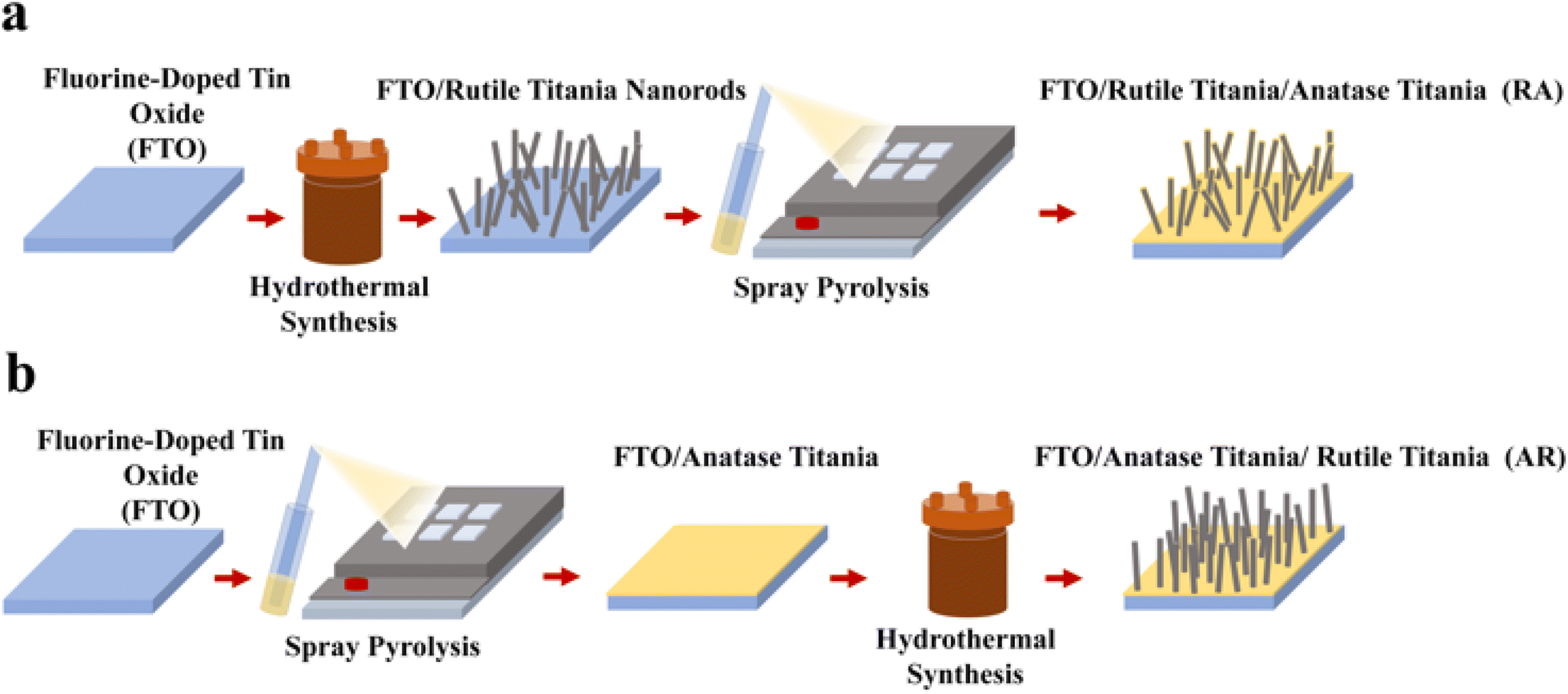 | ||
| Fig. 1 Schematics of synthesis methodology for (a) RA and (b) AR ETL structures. | ||
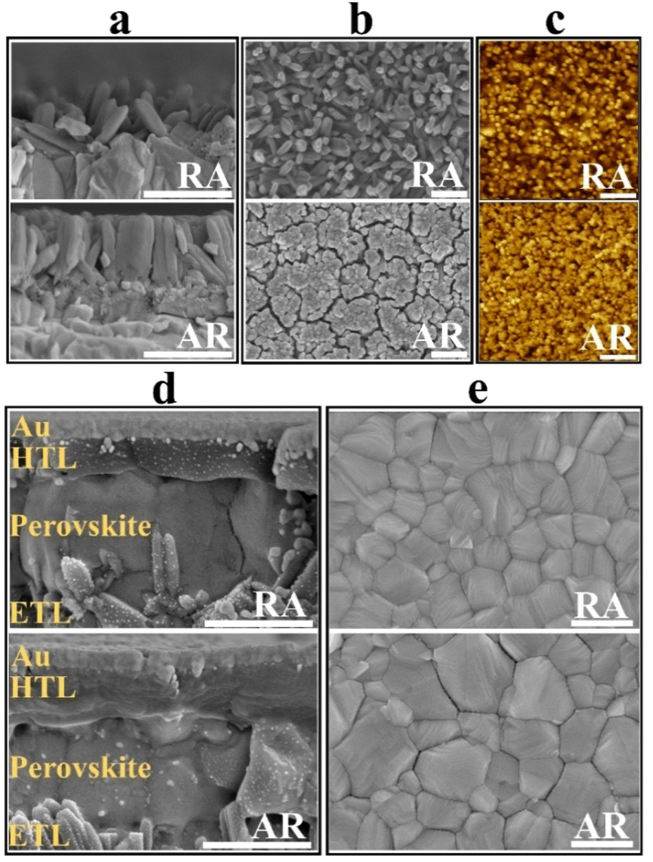 | ||
| Fig. 2 Cross section (a) and top view (b) SEM images, as well as the corresponding AFM images (c) of AR and RA structures, and (d) cross section SEM images of the full stack PSC devices as well as (e) the corresponding perovskite layer coating AR and RA structures. The scale bar in the SEM and AFM images denotes 500 nm and 1 μm, respectively. | ||
ETLs are then infiltrated/capped with the perovskite layer which has the nominal composition of (Cs5Rb5MA0.15FA0.75) Pb(I0.83Br0.17)3.37 The corresponding XRD patterns show analogous peaks for the perovskite layer filling ETL structures (Fig. S2a†). Full stack PSCs were assembled by using spiro-OMeTAD as the HTL and gold (Au) as a metallic contact. The cross-section SEM images of the resulting devices are presented in Fig. 2d, where the perovskite layer and the HTL show thickness values around 500 nm and 200 nm, respectively. Additionally, the top-view SEM images of the perovskite layer filling the ETL architectures (Fig. 2e) show enhanced crystallite size for the AR structure compared with that for RA. To dope the HTL, a two-stage doping process was utilized, whereby samples were left in a dark and dry desiccator (relative humidity below 10%) overnight prior to Au evaporation, followed by 15 hours of storage in 20% relative humidity under ambient light after the deposition of the metal contact. The effectiveness of our doping strategy was evaluated using space-charge limited current (SCLC) measurements on FTO/HTL/Au stacks (Fig. S2b†).
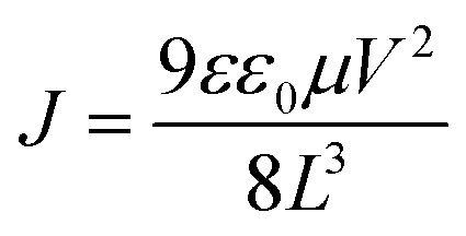
The mobility (μ) is calculated from the trap-free SCLC region using Mott–Gurney's square law according to eqn (1):
 | (1) |
Next, to measure photovoltaic (PV) metrics, J–V measurements were performed for both forward scan (FS) and reverse scan (RS) directions, at different scan rates of 100 mV s−1 and 10 mV s−1. In Fig. 3a–d, a comparison is made for PSCs based on each of the ETL structures, in terms of short-circuit current density (JSC), open-circuit voltage (VOC), fill factor (FF) and power conversion efficiency (PCE). Under 100 mV s−1, PSCs based on RA show higher JSC compared with their AR counterparts, while delivering similar values at lower scan rates (Fig. 3a). It should be noted that for both ETL structures the average of JSC between the two scan directions stays relatively similar. Under both scan rates, RA-based PSCs deliver higher VOC than those based on AR (Fig. 3b). Additionally, PSCs based on RA display closer VOC values between the two scan directions compared with AR-based PSCs. With regard to FF (Fig. 3c), slightly higher values are obtained upon utilization of AR as the ETL compared with those of RA-based PSCs. Finally, PSCs based on RA display higher PCEs than their AR counterparts (Fig. 3d). The PV metrics for each PSC type and the corresponding champion device in this case are summarized in Table S1.† It should be noted that since the composition, deposition and doping parameters corresponding to the HTL is not subject to variation, the observed changes can be majorly attributed to the ETL/perovskite interface.
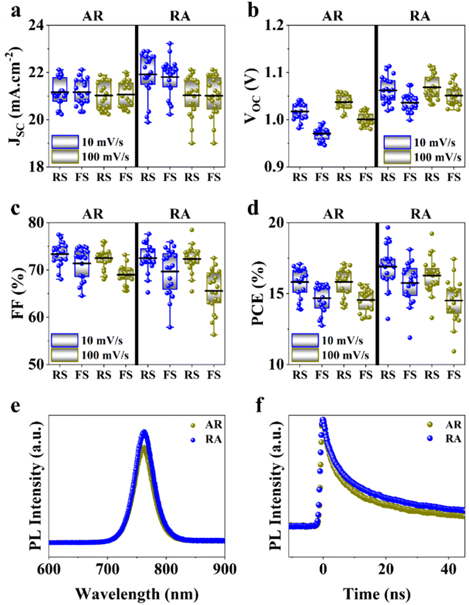 | ||
| Fig. 3 Comparison of the PV metrics in reverse scan (RS) and forward scan (FS) for PSCs based on AR and RA ETL structures: (a) JSC, (b) VOC, (c) FF, and (d) PCE, PL spectra with emission centered around 760 nm (e) and TRPL profiles (f) with the excitation wavelength set to 504 nm. | ||
Photoluminescence (PL) and time-resolved photoluminescence (TRPL) measurements were performed to gain insight into the ETL/perovskite interface. To isolate the effect of the ETL and its interface with the perovskite layer, PL/TRPL measurements were conducted on FTO/ETL/perovskite stacks, with the surface of the perovskite layer passivated using trioctylphosphine oxide (TOPO).39 The PL spectra of the perovskite layer coating AR and RA are presented in Fig. 3e, whereby RA shows a slightly enhanced PL intensity compared with AR. This observation is in line with higher VOC values recorded for the RA structure compared with those for AR (Fig. 3b). Fig. 3f shows the TRPL decay profiles for the two ETL configurations. The exponential decay curves were fitted using the biexponential decay model of eqn (2):40
 | (2) |
Additionally, the average lifetime (τave) is calculated using 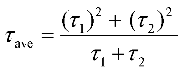 . The shorter τ1 and longer τ2 lifetime components are associated with non-radiative trap-assisted recombination and bulk radiative recombination, respectively.40 The corresponding fitting values of TRPL decay profiles are shown in Table 1. The smaller τ1 for AR compared with that for the RA configuration can be attributed to better charge extraction by the ETL,41 conforming to the trends observed for FF (Fig. 3c). The improved charge extraction of the AR structure can be ascribed to larger perovskite crystallite size, a smoother interface42 (Fig. 2c), and a favorable pathway for electron movement from rutile to anatase.43 In the literature, enhanced τ2 has been attributed to longer charge carrier lifetimes and hence longer diffusion lengths.44 Therefore, the higher τ2 for RA compared with that for AR is in line with their enhanced VOC. Overall, RA demonstrates a higher τave. We hypothesize that the higher conductivity of RA compared with that of the AR counterpart (Fig. S1c†) translates into a higher Fermi level, enabling this ETL to better match that of photoexcited electrons in the perovskite. The correlation between the absolute PL intensity and PV metrics such as FF and VOC is discussed thoroughly in the literature,45,46 and is out of the scope of this work.
| Sample | τ 1 (ns) | τ 2 (ns) | τ ave (ns) |
|---|---|---|---|
| AR | 4.22 ± 0.04 | 35.99 ± 0.30 | 32.65 |
| RA | 5.28 ± 0.05 | 48.34 ± 0.32 | 44.09 |
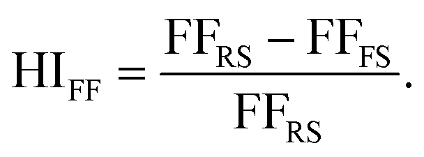
The external quantum efficiency (EQE) spectra for the best performing PSCs based on each ETL structure is presented in Fig. S3a.† A broad EQE plateau exceeding 80% is observed for both ETL structures between 400 nm and 750 nm. Additionally, the hysteresis index (HI) distribution for the PSCs utilized in this work is shown in Fig. S3b.† In the present study, the HI is defined based on the variation in the FF in the reverse and forward scan directions (denoted as FFRS and FFFS, respectively) according to eqn (3):47
 | (3) |
PSCs based on RA demonstrate mostly higher hysteresis compared with those based on AR. Conventionally, the metric of the HI has been utilized to gauge PSC performance. However, in recent years, questions have been raised with respect to the actual practically of the HI considering that it is merely a transient measure.48,49 In this work, we focus our attention on analyzing the locus of hysteresis as appearing on the representative J–V curves under 100 and 10 mV s−1 (Fig. 4). More specifically, AR shows divergence of the J–V curves starting shortly before VOC and extending to voltages exceeding that (Fig. 4a and c). In the case of RA (Fig. 4b and d), under both scan rates, the hysteresis locus appears to extend up to VOC and does not extend much beyond that. To better inspect the implications of the hysteresis locus with regard to charge carrier dynamics, EIS measurements were performed under 1 sun illumination and forward bias. As discussed previously, the major difference in the J–V curves for PSCs based on RA and AR is the range of voltages within which the FS and RS diverge. Therefore, we measured the evolution of EIS for both of the ETL structures when scanned from VOC to 1.4 V. The corresponding Nyquist plots for PSCs based on AR and RA are shown in Fig. 5. In the following, we first analyze the implication of EIS patterns obtained under open-circuit conditions through presenting a band diagram in Fig. 6a–c, which focuses on the ETL/perovskite interface.
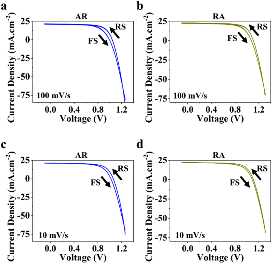 | ||
| Fig. 4 Representative current–voltage (J–V curves) measured under 100 mV s−1 and 10 mV s−1 in RS and FS for PSCs utilizing AR (a and c) and RA (b and d) as the ETL structure. | ||
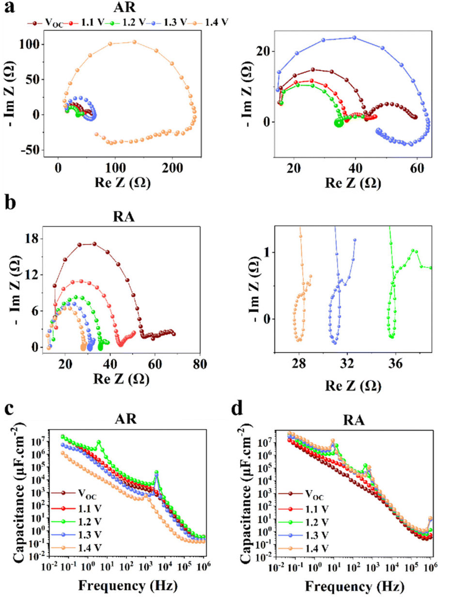 | ||
| Fig. 5 Comparison of Nyquist plots measured under 1 sun illumination and increasing forward bias for PSCs based on (a) AR and (b) RA as the ETL. The panels on the right column show the zoomed-in view of the adjacent panel on the left; C–f plots for PSCs based on (c) AR and (d) RA. | ||
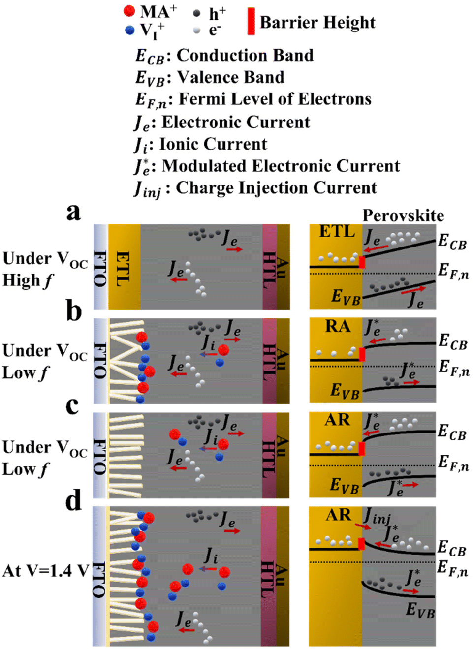 | ||
| Fig. 6 Charge carrier dynamics in PSCs under 1 sun illumination; (a) generalized scheme of the ETL/perovskite interface and band energy alignment in the high frequency region of EIS under VOC (before the effect of ionic charge appears), and under ionic pile up upon longer illumination times at lower frequencies for (b) RA and (c) AR ETL structures under VOC, and (d) the dynamics under increased forward bias leading to the appearance of a low frequency hook in the EIS spectra of AR. | ||
In principle, the electronic charge carrier dynamics in the high frequency range (106–103 Hz) of EIS measurements should be dominated only through the electronic conductivity of the perovskite bulk and that of interfaces, since this frequency range is too fast for ions to follow. The band diagram in this region (Fig. 6a) shows a built-in field across the perovskite layer which favors funneling of the electronic charge carriers into their respective transport layers (for both AR and RA structures, denoted as the ETL to represent the general case). At high frequency, such a band alignment is prevalent across the entire perovskite bulk film since the ionic effects take longer to modify the interfacial energetics. Note that our obtained Nyquist plots under VOC (Fig. 5a and b) display two full semicircles (at high and low frequencies). To fit the high frequency (HF) and low frequency (LF) arcs in the EIS patterns, we utilized an equivalent circuit shown in Fig. S4a,† where the series resistance element (RSeries) is connected in series with two RC branches (with R and C being resistance and capacitance, respectively), corresponding to the HF and LF arcs. The higher RSeries values of PSCs based on AR compared with those based on RA (Fig. S4b†) can be attributed to the lower conductivity of the AR structure as the ETL.
The observed capacitance response of the high frequency arc (CHF) is associated with the geometrical capacitance (Cg) and diverse dipolar mechanisms of the bulk perovskite material.50 The high and low frequency arc diameter (denoted as RHF and RLF, respectively) values are compared for different ETL structures as shown in Fig. S4c and Fig. S4d,† under open-circuit conditions. Notably, the observed trends for the two resistance parameters are in line with that of FF (Fig. 3c); PSCs based on RA display larger RHF and RLF compared to their AR counterparts. In the literature, both resistance parameters have been majorly attributed to recombination resistance.51,52 However, it can be readily seen from Fig. 3b that while the RA structure indeed shows a higher VOC than the AR structure (in accordance with the “recombination resistance” definition), their corresponding FF values are lower (Fig. 3c). Based on our observations, we attribute RHF and RLF to charge transfer resistance across the interface, similar to the conclusion drawn by Ebadi et al.27 Due to the higher conductivity of RA, a larger built-in field is expected to be generated across the perovskite bulk for the resulting PSCs (because of a larger difference between the Fermi levels in the ETL and HTL).
Such an effect would accelerate ionic movement towards contacts for the purpose of screening the field, resulting in an earlier appearance of flat band conditions in RA-based devices (Fig. 6b) compared with their AR counterparts (Fig. 6c). Once the ionic motion is triggered, the electronic current across the interface is no longer independent of ionic effects and is rather modulated through ionic migration and the resulting interfacial potential barrier height.30 Hence, in Fig. 6b and c, the electronic current at the interface is denoted as  (modulated electronic current) in the right column, while the bulk electronic current is denoted as Je in the left column. Reaching flat band conditions earlier leads to a larger portion of the built-in field to drop across the RA/perovskite interface which can enhance the rate of recombination between free holes and electrons at interfacial recombination sites as the predominant pathway.53 Hence, within the range of 0 V to VOC, the charge extraction landscape in PSCs based on RA would be dominated by recombination (to a larger extent than AR), which manifests in the deteriorated FF.
Next, to understand the divergence of J–V curves around VOC for AR-based structures, EIS measurements were conducted under 1 sun illumination and by increasing forward biases (VOC to 1.4 V). The resulting spectra (Fig. 5) demonstrate the appearance of inductance (in the form of a loop and a hook) in response to bias values larger than VOC. The occurrence of both such features indicates decreased differential resistance.15 However, since a loop appears in the mid-frequency range while a hook occurs in the lower frequency range, we are inclined to consider them as manifestation of different interfacial processes. There have been several experimental observations of inductance and theoretical understandings of this feature in PSCs.26,32,54–56 For both structures (Fig. 5a and b), increasing the voltage from VOC to 1.2 V leads to the reduction of RHF. Therefore, based on our interpretation of RHF as charge transfer resistance, its reduction as a function of increasing voltage can be taken as a sign of increased conductivity across the ETL/perovskite interface. In Fig. 5a and b, the inductive loop appears, in the mid-frequency range, earlier in the Nyquist plot for RA (1.1 V) than that of AR (1.2 V). Because of an earlier triggering of ionic migration, at a given time, a larger density of ionic charge is accumulated at the RA/perovskite interface. Increasing the forward bias further accelerates migration and accumulation,27 leading to higher accumulation of ionic charge at the interface than that in the perovskite bulk, eventually resulting in conduction band discontinuity (local downward and upward spikes) at the ETL/perovskite interface. As an implication of the higher interfacial doping density, the photoexcited electrons from the perovskite would be scattered at a higher rate in moving towards the ETL, leading to increased mobility,57 as has been shown previously for GaAs.58 This, in turn, decreases resistance which results in the appearance of an inductive loop in the Nyquist plot. Conversely, based on our hypothesis, if the photogenerated electrons experience a consistent movement in one direction (for example consistent downward movement from the perovskite into the ETL without encountering spikes), then an inductive loop would not appear (e.g., Nyquist plots for both ETLs under VOC). Correspondingly, at 1.1 V, ionic pile-up and hence band discontinuity at the RA/perovskite interface are already considerable enough resulting in the observed inductive loop. Therefore, the reason for AR showing a delayed inductive loop compared with RA can be its slower pace of ionic movement which would require larger applied voltages to create comparable ionic accumulation with those of RA at a given doping density. Notably, the two ETL structures diverge considerably for 1.3 V and 1.4 V; while RA still shows decreased RHF, AR demonstrates a drastic increase of RHF in addition to displaying a hook in the low frequency region. The coupled increase of RHF and the appearance of a hook in the Nyquist plots can be attributed to band inversion at the AR/perovskite interface, as illustrated in Fig. 6d. Band inversion, due to dipole formation, has been suggested to take place in earlier59 as well as more recent studies.26 To gain further insight, capacitance vs. frequency (C–f) representations are also provided, as shown in Fig. 5b and c. In the C–f plots, low frequency capacitance is associated with the surface capacitance of accumulated charge at the interface and is termed surface capacitance (Cs).20 The frequencies at which the spikes in capacitance occur correlate with those of both the mid- and low-frequency inductance, as observed from the corresponding Nyquist plots (Fig. 5a and b). For RA, the Cs continuously increases from VOC to 1.4 V. Conversely, for AR, Cs at 1.4 V displays the lowest value among all the studied biases (about an order of magnitude lower than the value obtained under VOC).
Next, we set to understand the connotations of low frequency inductance as observed in the Nyquist plots of AR, as shown in Fig. 5a. If we assume that the AR surface has a lower capacity for accommodating positively charged ionic species than the RA surface, then it would follow that due to the increased concentration of accumulated ionic species (because of increased forward bias), the resulting interfacial p-doping density in the perovskite would be sufficient to induce band inversion in the perovskite/AR interface. Therefore, for a given ETL, there would be a threshold of the accumulated ionic density within the perovskite layer before it can be considered p-doped and induce inversion of the bands as a result. In this interpretation, the inductive loop, which appears as a semicircle in the fourth quadrant, is indicative of electron injection from the ETL into the perovskite. Concomitantly, the apparent negative differential resistance associated with low frequency inductance is in fact indicative of charge carrier movement in the opposite direction of what gives rise to the HF and LF semicircles. Therefore, the appearance of low-frequency inductance in the Nyquist plots of AR can be indicative of inverted bands at the perovskite interface, resulting in the diminished VOC in FS. Overall, our interpretation of hysteresis in PSCs is in line with the results of previous works,27–30 attributing hysteresis and low frequency dynamics to the out-of-phase electronic recombination current amplified through the out-of-phase ionic current.
Moreover, we attempted to establish a correlation between the hysteresis locus and recombination regime. As we argued earlier, conductivity can play a key role in determining band alignment at the interface, whereby for a higher n-doped ETL, the perovskite can afford to have a larger ionic pile up at the interface before the perovskite/ETL interface can be considered a sufficiently doped n–p heterojunction with the bands becoming inverted on the p side (perovskite) as shown in Fig. 6d. PSCs based on AR demonstrate diminished VOC in FS (more pronounced compared with RA), which, we believe, stems from the conductivity of the ETL. Specifically, conductivity determines how fast the ionic movement across the perovskite layer is initiated. Therefore, since it was shown earlier that AR has lower electronic conductivity, meaning the free accumulated electrons in AR cannot be dissipated from the interface towards the ETL bulk as fast as those in RA, in the presence of inverted bands (under 1.3 and 1.4 V as shown in Fig. 6d), non-radiative recombination (between electrons in the ETL and holes in the perovskite, close to the interface) would be enhanced leading to reduced VOC in FS, while under RS, the bands in AR would recover towards a more favorable alignment (Fig. 6c), due to the dissipation of positively charged ionic species towards the HTL, therefore giving rise to larger VOC values compared with those for FS. Additionally, based on the obtained results for PSCs based on RA, we can conclude that a mid-frequency loop has a less detrimental effect on the VOC measured in FS (Table S1†). Hence, depending on the band alignment under which recombination takes place, the locus of hysteresis can be varied; recombination under inverted band alignment leads to widening of the J–V curves around VOC and exceeding voltages (Fig. 4a and c), while recombination under flat band conditions results in J–V divergence up to VOC (Fig. 4b and d).
Finally, the shelf stability of the non-encapsulated PSCs was tested by storing them for 200 hours under darkness and 25% relative humidity. The resulting distribution of PV metrics is shown in Fig. S5 and summarized in Table S2.† The average PCE after storage is seen to slightly drop for both ETL architectures (AR and RA) under both scan rates and directions. The most prominent change after storage relates to the reduction of JSC. The VOC also is seen to decrease upon storage in the case of RA-based PSCs, but surprisingly it increases after storage (except for 10 mV s−1 which renders very close values) in the case of the AR architecture. The FF values remain relatively similar under most scan conditions. The observed divergence in the evolution of VOC under storage can be attributed to the ETL/perovskite interface since the HTL-related parameters were not subjected to change.
Conclusions
In summary, we have studied the hysteresis locus in PSCs and the origin of inductive features by analyzing the Nyquist plot patterns under 1 sun illumination. The measurements were performed on ETL architectures synthesized through a combination of hydrothermal synthesis and spray pyrolysis, rendering AR and RA structures. The high and low frequency resistance parameters under open-circuit conditions from Nyquist plots were attributed to charge transfer resistance across perovskite interfaces. Importantly, in the EIS measurements performed under increasing forward bias, inductive features (loop and hook) were observed in the Nyquist plot. We attributed the mid-frequency loop to increased scattering of photoexcited electrons due to enhanced interfacial doping density (because of increased ionic accumulation at the ETL interface compared with that of the perovskite bulk). The occurrence of a low frequency inductive hook in the Nyquist plots of PSCs based on both AR structures was attributed to the inversion of the perovskite bands at the ETL interface. It was postulated that the higher conductivity of a given ETL structure could enhance the pace of ionic migration from the perovskite towards interfaces resulting in accumulation of ionic species that consequently affects the band alignment for electronic charge transfer to respective contacts due to ionic-electronic current amplification. Additionally, we pointed to the conductivity of a given ETL as a potential cause for observing low frequency inductance. We believe that the low frequency hook observed in the Nyquist plots of PSCs is directly related to diminished VOC values in the forward scan direction.Author contributions
Rana Yekani: conceptualization, methodology, AFM, PV, PL and EIS analyses, investigation, visualization, writing – original draft, review & editing, and resources. Hsien-chieh Chiu: writing – review and editing, resources. Dallas Strandell: TRPL analysis, writing – review and editing. Zhuoran Wang: writing – review and editing and resources. Stéphanie Bessette and Raynald Gauvin: SEM analysis and writing – review and editing. George P. Demopoulos: writing – review and editing, resources, and supervision.Conflicts of interest
There are no conflicts of interest to declare.Acknowledgements
This work was funded by the Natural Sciences & Engineering Research Council of Canada (NSERC) through a strategic project and discovery grants. Additional support through the McGill Sustainability Systems Initiative (MSSI) and the McGill Engineering Doctoral Award (MEDA) programs is acknowledged.References
- A. Kojima, K. Teshima, Y. Shirai and T. Miyasaka, J. Am. Chem. Soc., 2009, 131, 6050–6051 CrossRef CAS PubMed.
- J. Jeong, M. Kim, J. Seo, H. Lu, P. Ahlawat, A. Mishra, Y. Yang, M. A. Hope, F. T. Eickemeyer and M. Kim, Nature, 2021, 592, 381–385 CrossRef CAS PubMed.
- J. J. Yoo, G. Seo, M. R. Chua, T. G. Park, Y. Lu, F. Rotermund, Y.-K. Kim, C. S. Moon, N. J. Jeon, J.-P. Correa-Baena, V. Bulović, S. S. Shin, M. G. Bawendi and J. Seo, Nature, 2021, 590, 587–593 CrossRef CAS PubMed.
- S. D. Stranks, G. E. Eperon, G. Grancini, C. Menelaou, M. J. Alcocer, T. Leijtens, L. M. Herz, A. Petrozza and H. J. Snaith, Science, 2013, 342, 341–344 CrossRef CAS PubMed.
- S. De Wolf, J. Holovsky, S.-J. Moon, P. Löper, B. Niesen, M. Ledinsky, F.-J. Haug, J.-H. Yum and C. Ballif, J. Phys. Chem. Lett., 2014, 5, 1035–1039 CrossRef CAS PubMed.
- G. Xing, N. Mathews, S. Sun, S. S. Lim, Y. M. Lam, M. Grätzel, S. Mhaisalkar and T. C. Sum, Science, 2013, 342, 344–347 CrossRef CAS PubMed.
- B. Das, Z. Liu, I. Aguilera, U. Rau and T. J. M. A. Kirchartz, Mater. Adv., 2021, 2, 3655–3670 RSC.
- H. J. Snaith, A. Abate, J. M. Ball, G. E. Eperon, T. Leijtens, N. K. Noel, S. D. Stranks, J. T. Wang, K. Wojciechowski and W. Zhang, J. Phys. Chem. Lett., 2014, 5, 1511–1515 CrossRef CAS PubMed.
- W. Tress, N. Marinova, T. Moehl, S. M. Zakeeruddin, M. K. Nazeeruddin and M. Grätzel, Energy Environ. Sci., 2015, 8, 995–1004 RSC.
- S. Meloni, T. Moehl, W. Tress, M. Franckevičius, M. Saliba, Y. H. Lee, P. Gao, M. K. Nazeeruddin, S. M. Zakeeruddin, U. Rothlisberger and M. Graetzel, Nat. Commun., 2016, 7, 10334 CrossRef CAS PubMed.
- M. Abdi-Jalebi, Z. Andaji-Garmaroudi, S. Cacovich, C. Stavrakas, B. Philippe, J. M. Richter, M. Alsari, E. P. Booker, E. M. Hutter, A. J. Pearson, S. Lilliu, T. J. Savenije, H. Rensmo, G. Divitini, C. Ducati, R. H. Friend and S. D. Stranks, Nature, 2018, 555, 497–501 CrossRef CAS PubMed.
- M. Saliba, T. Matsui, K. Domanski, J.-Y. Seo, A. Ummadisingu, S. M. Zakeeruddin, J.-P. Correa-Baena, W. R. Tress, A. Abate, A. Hagfeldt and M. Grätzel, Science, 2016, 354, 206–209 CrossRef CAS PubMed.
- S. van Reenen, M. Kemerink and H. J. Snaith, J. Phys. Chem. Lett., 2015, 6, 3808–3814 CrossRef CAS PubMed.
- P. Calado, A. M. Telford, D. Bryant, X. Li, J. Nelson, B. C. O'Regan and P. R. F. Barnes, Nat. Commun., 2016, 7, 13831 CrossRef CAS PubMed.
- J. Ye, M. M. Byranvand, C. O. Martínez, R. L. Z. Hoye, M. Saliba and L. Polavarapu, Angew. Chem., Int. Ed., 2021, 60, 21636–21660 CrossRef CAS PubMed.
- D.-H. Kang and N.-G. Park, Adv. Mater., 2019, 31, 1805214 CrossRef PubMed.
- P. Liu, W. Wang, S. Liu, H. Yang and Z. Shao, Adv. Energy Mater., 2019, 9, 1803017 CrossRef.
- E. Von Hauff and D. Klotz, J. Mater. Chem. C, 2022, 10, 742–761 RSC.
- A. Guerrero, G. Garcia-Belmonte, I. Mora-Sero, J. Bisquert, Y. S. Kang, T. J. Jacobsson, J.-P. Correa-Baena and A. Hagfeldt, J. Phys. Chem. C, 2016, 120, 8023–8032 CrossRef CAS.
- I. Zarazua, J. Bisquert and G. Garcia-Belmonte, J. Phys. Chem. Lett., 2016, 7, 525–528 CrossRef CAS PubMed.
- J. Bisquert and A. Guerrero, J. Am. Chem. Soc., 2022, 144, 5996–6009 CrossRef CAS PubMed.
- C. Gonzales, A. Guerrero and J. Bisquert, J. Phys. Chem. C, 2022, 126, 13560–13578 CrossRef CAS.
- E. Hernández-Balaguera and J. Bisquert, ACS Energy Lett., 2022, 7, 2602–2610 CrossRef.
- L. Munoz-Diaz, A. J. Rosa, A. Bou, R. S. Sánchez, B. Romero, R. A. John, M. V. Kovalenko, A. Guerrero and J. Bisquert, Front. Energy Res., 2022, 911 Search PubMed.
- F. Fabregat-Santiago, M. Kulbak, A. Zohar, M. Vallés-Pelarda, G. Hodes, D. Cahen and I. Mora-Seró, ACS Energy Lett., 2017, 2, 2007–2013 CrossRef CAS.
- E. Ghahremanirad, A. Bou, S. Olyaee and J. Bisquert, J. Phys. Chem. Lett., 2017, 8, 1402–1406 CrossRef CAS PubMed.
- F. Ebadi, N. Taghavinia, R. Mohammadpour, A. Hagfeldt and W. Tress, Nat. Commun., 2019, 10, 1574 CrossRef PubMed.
- A. Pockett, G. E. Eperon, N. Sakai, H. J. Snaith, L. M. Peter and P. J. Cameron, Phys. Chem. Chem. Phys., 2017, 19, 5959–5970 RSC.
- D. A. Jacobs, H. Shen, F. Pfeffer, J. Peng, T. P. White, F. J. Beck and K. R. Catchpole, J. Appl. Phys., 2018, 124, 225702 CrossRef.
- D. Moia, I. Gelmetti, P. Calado, W. Fisher, M. Stringer, O. Game, Y. Hu, P. Docampo, D. Lidzey, E. J. E. Palomares and E. Science, Energy Environ. Sci., 2019, 12, 1296–1308 RSC.
- Y. Feng, J. Bian, M. Wang, S. Wang, C. Zhang, Q. Dong, B. Zhang and Y. Shi, Mater. Res. Bull., 2018, 107, 74–79 CrossRef CAS.
- M. Anaya, W. Zhang, B. C. Hames, Y. Li, F. Fabregat-Santiago, M. E. Calvo, H. J. Snaith, H. Miguez and I. Mora-Sero, J. Mater. Chem. C, 2017, 5, 634–644 RSC.
- B. Liu and E. S. Aydil, J. Am. Chem. Soc., 2009, 131, 3985–3990 CrossRef CAS PubMed.
- M. Saliba, J.-P. Correa-Baena, C. M. Wolff, M. Stolterfoht, N. Phung, S. Albrecht, D. Neher and A. Abate, Chem. Mater., 2018, 30, 4193–4201 CrossRef CAS.
- B. Liu and E. S. Aydil, J. Am. Chem. Soc., 2009, 131, 3985–3990 CrossRef CAS PubMed.
- J. Kalb, A. Folger, E. Zimmermann, M. Gerigk, B. Trepka, C. Scheu, S. Polarz and L. Schmidt-Mende, Surf. Interfaces, 2019, 15, 141–147 CrossRef CAS.
- M. Saliba, T. Matsui, K. Domanski, J.-Y. Seo, A. Ummadisingu, S. M. Zakeeruddin, J.-P. Correa-Baena, W. R. Tress, A. Abate and A. J. S. Hagfeldt, Science, 2016, 354, 206–209 CrossRef CAS PubMed.
- S. G. Kim, T. H. Le, T. de Monfreid, F. Goubard, T. T. Bui and N. G. Park, Adv. Mater., 2021, 33, 2007431 CrossRef CAS PubMed.
- I. L. Braly, D. W. deQuilettes, L. M. Pazos-Outón, S. Burke, M. E. Ziffer, D. S. Ginger and H. W. Hillhouse, Nat. Photonics, 2018, 12, 355–361 CrossRef CAS.
- D. Bi, C. Yi, J. Luo, J.-D. Décoppet, F. Zhang, S. M. Zakeeruddin, X. Li, A. Hagfeldt and M. Grätzel, Nat. Energy, 2016, 1, 16142 CrossRef CAS.
- J. Chen, J. Y. Seo and N. G. Park, Adv. Energy Mater., 2018, 8, 1702714 CrossRef.
- G. Kakavelakis, T. Maksudov, D. Konios, I. Paradisanos, G. Kioseoglou, E. Stratakis and E. Kymakis, Adv. Energy Mater., 2017, 7, 1602120 CrossRef.
- D. O. Scanlon, C. W. Dunnill, J. Buckeridge, S. A. Shevlin, A. J. Logsdail, S. M. Woodley, C. R. A. Catlow, M. Powell, R. G. Palgrave and I. P. Parkin, Nat. Mater., 2013, 12, 798–801 CrossRef CAS PubMed.
- S.-G. Kim, J. Chen, J.-Y. Seo, D.-H. Kang and N.-G. Park, ACS Appl. Mater. Interfaces, 2018, 10, 25372–25383 CrossRef CAS PubMed.
- M. Stolterfoht, P. Caprioglio, C. M. Wolff, J. A. Márquez, J. Nordmann, S. Zhang, D. Rothhardt, U. Hörmann, Y. Amir and A. Redinger, Energy Environ. Sci., 2019, 12, 2778–2788 RSC.
- T. Kirchartz, J. A. Márquez, M. Stolterfoht and T. Unold, Adv. Energy Mater., 2020, 10, 1904134 CrossRef CAS.
- E. L. Unger, A. Czudek, H.-S. Kim and W. Tress, in Characterization Techniques for Perovskite Solar Cell Materials, Elsevier, 2020, pp. 81–108 Search PubMed.
- S. N. Habisreutinger, N. K. Noel and H. J. Snaith, ACS Energy Lett., 2018, 3, 2472–2476 CrossRef CAS.
- V. M. Le Corre, J. Diekmann, F. Peña-Camargo, J. Thiesbrummel, N. Tokmoldin, E. Gutierrez-Partida, K. P. Peters, L. Perdigón-Toro, M. H. Futscher and F. Lang, Sol. RRL, 2022, 6, 2100772 CrossRef CAS.
- A. Pockett, G. E. Eperon, T. Peltola, H. J. Snaith, A. Walker, L. M. Peter and P. J. Cameron, J. Phys. Chem. C, 2015, 119, 3456–3465 CrossRef CAS.
- I. Zarazua, G. Han, P. P. Boix, S. Mhaisalkar, F. Fabregat-Santiago, I. Mora-Sero, J. Bisquert and G. Garcia-Belmonte, J. Phys. Chem. Lett., 2016, 7, 5105–5113 CrossRef CAS PubMed.
- J.-P. Correa-Baena, S.-H. Turren-Cruz, W. Tress, A. Hagfeldt, C. Aranda, L. Shooshtari, J. Bisquert and A. Guerrero, ACS Energy Lett., 2017, 2, 681–688 CrossRef CAS.
- M. Stolterfoht, C. M. Wolff, J. A. Márquez, S. Zhang, C. J. Hages, D. Rothhardt, S. Albrecht, P. L. Burn, P. Meredith and T. J. N. E. Unold, Nat. Energy, 2018, 3, 847–854 CrossRef CAS.
- M. Ulfa, T. Zhu, F. Goubard and T. Pauporté, J. Mater. Chem. A, 2018, 6, 13350–13358 RSC.
- A. O. Alvarez, R. Arcas, C. A. Aranda, L. Bethencourt, E. Mas-Marza, M. Saliba and F. Fabregat-Santiago, J. Phys. Chem. Lett., 2020, 11, 8417–8423 CrossRef CAS PubMed.
- F. Fabregat-Santiago, M. Kulbak, A. Zohar, M. Vallés-Pelarda, G. Hodes, D. Cahen and I. Mora-Seró, ACS Energy Lett., 2017, 2, 2007–2013 CrossRef CAS.
- D. A. Neamen, Semiconductor physics and devices: basic principles, McGraw-hill, 2003 Search PubMed.
- M. J. P. R. Cardona, Phys. Rev., 1961, 121, 752 CrossRef.
- A. Guerrero, J. You, C. Aranda, Y. S. Kang, G. Garcia-Belmonte, H. Zhou, J. Bisquert and Y. Yang, ACS Nano, 2016, 10, 218–224 CrossRef CAS PubMed.
Footnote |
| † Electronic supplementary information (ESI) available. See DOI: https://doi.org/10.1039/d2nr05836g |
| This journal is © The Royal Society of Chemistry 2023 |