
Enhancement of spontaneous emission from CdSe/ZnS quantum dots through silicon nitride photonic crystal cavity based on miniaturized bound states in the continuum
Guixin
Qiu†
a,
Dunzhao
Wei†
a,
Zhuojun
Liu
 *b and
Jin
Liu
a
*b and
Jin
Liu
a
aState Key Laboratory of Optoelectronic Materials and Technologies, School of Physics, Sun Yat-sen University, Guangzhou 510275, China
bState Key Laboratory for Mesoscopic Physics and Frontiers Science Center for Nano-optoelectronics, School of Physics, Peking University, Beijing 100871, China. E-mail: zhuojunliu@pku.edu.cn
First published on 25th January 2023
Abstract
Colloidal CdSe/ZnS quantum dots (QDs) exhibit excellent optical properties for wide potential applications in light-emitting diodes, solar concentrators, and single-photon sources. However, the ultra-thin films with low concentration of QDs still encounter inefficient photoluminescence (PL) and poor directionality of radiation, which need to be enhanced using nanophotonics device designs. Here we design and experimentally demonstrate an on-substrate silicon nitride (SiN) photonic crystal (PhC) microcavity encapsulated by a layer of PMMA hosting CdSe/ZnS QDs. The miniaturized bound states in the continuum (BIC) supported by our structures, provide high-Q resonant modes with highly-directional emission patterns. Experimental results show that the BIC mode in the microcavity has a Q-factor up to 7000 owing to the symmetric refractive index distribution along the Z-direction, rendering 8.5-fold enhancement of PL intensity and 8.4-fold acceleration of radiative emission rate. Our work provides a practical way for constructing efficient on-chip surface-emitting light sources on silicon-based integrated photonic devices.
1 Introduction
Colloidal CdSe/ZnS quantum dots (QDs) have been regarded as a novel class of light-conversion materials owing to their easy synthesis via low-cost wet chemistry techniques and excellent optical properties, i.e., bright, stable and size-dependent tunable photoluminescence (PL) in the visible spectrum at room temperature.1,2 They have been widely used as an active medium for constructing optical devices such as light emitting diodes (LEDs), solar concentrators, lasers, etc.3–7 The thin-film QD active layers of the above optical devices generally suffer from inefficient PL and poor directivity of radiation. In order to increase performances of ultra-thin films with low concentration of QDs, many efforts have been made to introduce QDs into integrated photonic devices for enhancing their interaction with light.8–12 Microcavities formed by defects in photonic crystal (PhC) slab or plasmonic structures have been used to couple with these QDs to increase their emission efficiencies.13–17,43 However, most of these traditional PhC defect cavities need to open the complete photonic bandgap for the in-plane light confinement. In order to obtain a high refractive index contrast, the sacrificial layer needs to be removed to form a suspended PhC membrane, which leads to a lack of mechanical and thermal stability. The suspended cavities are fragile during the spin-coating process of the colloidal QDs. In addition, the emissions from PhC defect cavities operating below the light cone are within a relatively large divergence angle. Therefore, it often requires a high numerical aperture (NA) lens to efficiently collect the emissions.In recent years, a new kind of on-chip cavity based on the so-called bound states in the continuum (BICs) in PhC slabs have been attracting extensive attention due to their nonlocal high-Q resonant mode and topological-protected far-field radiation.18–22 From the view of band structures of a PhC slab, the BIC modes operate above the light cone, but they are nonradiative with an infinite Q-factor owing to symmetry protection at the Γ-point or destructive interference between different radiation channels. Even without a complete photonic bandgap, such BIC modes can still achieve high Q-factors and efficient confinements in a low index contrast environment. As the requirement of refractive index contrast is relaxed, the supporting substrate can be used to improve both the mechanical and thermal stabilities of PhC membranes.23,24 Amazingly, triggering a transition from BICs to quasi-BICs allows the resonant modes to couple into the light cone, which have been used to construct passive or active integrated photonic devices, including optical sensors,25,26 lasers,27,28 quantum sources,29–32etc. Furthermore, the BIC mode at the Γ-point has a significant advantage in terms of efficient excitation and extraction in the vertical direction. By spin-coating a layer of active medium, e.g. colloidal QDs, on the corresponding PhC slab, these BIC modes formed directional PL emission or lasing.33,34 Recently, a heterostructure PhC cavity formed by tuning the hole radii has been proposed to further improve the power densities of the BIC mode, which successfully truncate the size of the BIC mode and enhance the light–matter interaction.35,36 However, compared with the suspended cavities, this scheme lacks the symmetric distribution of refractive index along the vertical direction, which is a great help to improve the Q-factor of the BIC mode.37,38
Here we design and fabricate an on-substrate heterostructure silicon nitride (SiN) PhC cavity encapsulated by a layer of polymethyl methacrylate (PMMA) with CdSe/ZnS QDs doping inside, which features a miniaturized high-Q BIC mode and strongly enhanced PL emission with highly directional radiation patterns. These advantages come from two facts: the heterostructure PhC slab includes two regions, i.e. a core region supporting BIC modes and a boundary region as mirrors for lateral confinement; the encapsulated QDs-doping PMMA provide nearly the same refractive index as that of a silicon oxide (SiO2) substrate, thus a symmetric distribution of refractive index along the vertical direction is formed. In the experiment, a PL peak with 8.5-fold enhancement is achieved, attributed to a Q-factor up to 7000, and the measurement of time-resolved PL decay shows that the spontaneous emission rate of CdSe/ZnS QDs was significantly enhanced by a factor of 8.4. Our work provides an easy but practical way for creating efficient surface-emitting light sources on passive integrated photonic devices.
2 Results
2.1 Cavity design
Fig. 1(a) shows the schematic of the device. A SiN PhC slab with a thickness h, on the SiO2 substrate, is encapsulated by a layer of PMMA. The transparent window of SiN material in the visible spectrum avoids absorption loss of the excitation and emission light. The SiN heterostructure cavity is composed of two regions, where a core region with hole radius rc is surrounded by a boundary region with smaller hole radius rb. Both are formed by a hexagonal lattice of holes with the same lattice constant a. Their corresponding sizes are defined by the number of layers of holes in each region, labeled Nc for the core region and Nb for the boundary region. The Γ-point BIC mode is supported by the core region, and the boundary region with smaller hole radius confines the mode as effectively as lateral mirrors. The PMMA mixing with CdSe/ZnS QDs covers the top of the SiN slab. Since the refractive index of PMMA (n ≈ 1.47) is almost the same as that of SiO2 (n ≈ 1.45),39 the device provides a symmetric refractive index distribution in the vertical direction to realize a better BIC mode at the Γ-point. Besides, the close contact between the uniform layer of PMMA and the SiN slab ensures sufficient coupling between the doping QDs and the resonant mode, mainly confined in the SiN slab. Targeting at a resonant wavelength around 660 nm, the parameters of the device were set as: a = 650 nm, h = 185 nm, Nc = 12, Nb = 50, rc = 145 nm, rb = 140 nm. Fig. 1(b) shows the photonic band structures of the two regions with the above parameters obtained by the COMSOL Multiphysics software. Here we should note that the band structures were calculated by extending the core and boundary regions into infinite ones. The red dotted curves in Fig. 1(b) represent three TE-like band structures of the boundary region, in which an incomplete band gap exists near the Γ-point as indicated by the shaded area in Fig. 1(b). Especially, the Γ-point of the lowest band at the first Brillouin zone is symmetry-protected, resulting in a non-radiative BIC mode embedded in the radiative light cone. Theoretically, the Γ-point BIC mode has an infinite Q-factor if the slab is large enough, providing a powerful way to confine out-of-plane optical fields.20,40 The increase of hole radius would raise the whole band structure without distorting the Γ-point BIC mode. We focus on the behavior of the Γ-point BIC mode, so only the lowest band (solid blue line) of the core region is plotted in Fig. 1(b). The Γ-point BIC mode of the core region thus lies in the incomplete bandgap of the boundary region, which prohibits it from coupling with the similar modes in the boundary region. In such a heterostructure configuration, the cavity mode can be confined vertically in the slab by the high-Q BIC and laterally in the core region by the mode gap. Fig. 1(c) shows the dependence of the Q-factor (red line) and mode volume (green line) on the core region size Nc with a fixed Nb = 50, calculated by the finite-difference time-domain (FDTD) method. The Q-factor is positively correlated with Nc and the mode volume reached its minimum at Nc = 12. In our design, Nc = 12 corresponds to a size smaller than 10 μm × 10 μm. In addition, the Q-factor depending on boundary region size Nb with a fixed Nc = 12 is also calculated in Fig. 1(d), which is positively related to Nb and becomes saturated with Nb > 40, so that the boundary region plays an important role in the lateral confinement. The parameters at Nc = 12 and Nb = 50 reduce the mode volume as much as possible while maintaining a Q-factor up to 22![[thin space (1/6-em)]](https://www.rsc.org/images/entities/char_2009.gif) 200. The corresponding in-plane intensity distribution of the BIC mode is well confined in the cavity region, as shown in Fig. 1(e). Our design provides a unique way to minimize BIC-based photonic devices for enhancing the interaction between the BIC mode and the doping CdSe/ZnS QDs. The surface normal far-field emission pattern in the inset of Fig. 1(e) indicates that nearly all the emitted light is concentrated within the divergence angle of 5°. Therefore, the emitted light can be easily collected through a small numerical aperture lens.
200. The corresponding in-plane intensity distribution of the BIC mode is well confined in the cavity region, as shown in Fig. 1(e). Our design provides a unique way to minimize BIC-based photonic devices for enhancing the interaction between the BIC mode and the doping CdSe/ZnS QDs. The surface normal far-field emission pattern in the inset of Fig. 1(e) indicates that nearly all the emitted light is concentrated within the divergence angle of 5°. Therefore, the emitted light can be easily collected through a small numerical aperture lens.
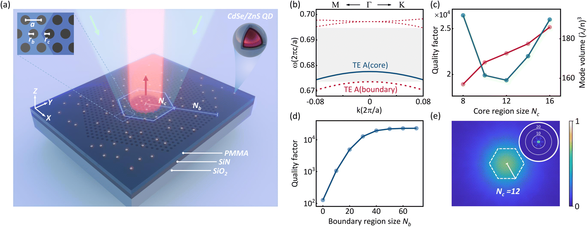 | ||
| Fig. 1 Working principle of miniaturized BIC-based surface-emitting light source. (a) Schematic of the miniaturized BIC-based light source. It consists of a heterostructure SiN PhC slab embedded between a SiO2 substrate and a top layer of PMMA mixed with CdSe/ZnS QDs. The inset shows a zoomed-in view of the separation between the core and boundary regions in the SiN PhC slab. A green light is used to excite the PL spectra which is surface-emitting along the vertical direction. (b) Calculated photonic band structures of the core region and boundary region around the Γ-point. The TE band in the core region (blue curve) is embedded in the band gap of the boundary region (red dotted curves). (c) Simulated Q-factors (red points) and mode volume (green points) dependences on core region size Nc with a fixed Nb = 50. (d) Simulated Q-factors dependence on boundary region size Nb with a fixed Nc = 12. (e) Intensity distribution of the BIC mode with a resonant wavelength of 680 nm when Nc = 12, Nb = 50. The inset shows the far-field emission pattern of the cavity, where the white concentric circles correspond to 10°, 20°, 30° from the inner one to the outer one, respectively. | ||
2.2 Sample fabrication and characterization setup
Firstly, a 185 nm-thick SiN membrane was grown on a 3 μm thick SiO2 layer with a silicon substrate via inductively coupled plasma chemical vapor deposition (ICPCVD). A 400 nm ARP-6200 electron beam resist was spin-coated on top of the SiN membrane, and then patterned by electron-beam lithography (Raith Vistec EBPG5000+ 100 kV). The pattern was transferred to the SiN membrane using reactive ion etching (RIE) with a CHF3/O2 plasma. Finally, after cleaning using a gentle oxygen plasma descum process to remove the residue, the sample was encapsulated by spinning a ∼600 nm-thick layer of CdSe/ZnS QDs-doped PMMA with 4000 rpm for 1 minute and then baked at a temperature of 60 °C for 3 minutes. The key points for the preparation of CdSe/ZnS QDs-doped PMMA are as follows: surface modification was carried out to improve the polarity of the synthetic CdSe/ZnS QDs with PL emission in the range 630 nm to 710 nm, so that they could be dissolved in anisole for quantification and mixed uniformly with PMMA (MicroChem 950PMMA A7, purchased from Taizhou SUNANO New Energy Co., Ltd.). Although the pure CdSe/ZnS QDs have a higher refractive index of ∼2.1, their low concentration in PMMA had little influence on the refractive index of the PMMA layer. The bottom of Fig. 2 shows the scanning electron microscopy (SEM) image of the fabricated BIC-based microcavity before spinning the PMMA, where the borders between the core and boundary regions are indicated by white dashed lines. The amplified SEM image in the top right corner shows that the air-holes are regular circular shape with vertical and smooth-sided walls.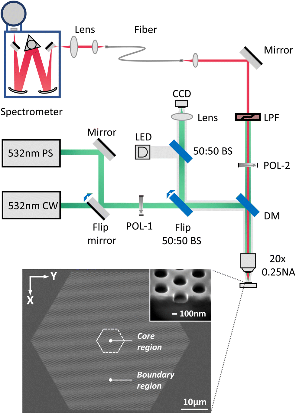 | ||
| Fig. 2 Characterization setup. Top: The home-built confocal microscope PL system. PS: picosecond-pulsed laser, CW: continuous-wave laser, POL: polarizer, BS: beam splitter, LED: light emitting diode, CCD: charge coupled device, DM: dichroic mirror, LPF: 620 nm long pass filter. Bottom: scanning electron microscopy (SEM) image of the fabricated BIC-based microcavity before spinning the PMMA, where the borders between the core and boundary regions are indicated by white dashed lines. Inset: cross-section of air-holes. | ||
The PL measurement was performed using a home-built confocal microscope PL system (Fig. 2, top). A continuous wave (CW) laser and a picosecond-pulsed laser working at a wavelength of 532 nm were used as the excitation lasers to measure the resonant PL spectrum and time-resolved PL spectrum, respectively. They could be switched through a flip mirror. The excitation laser passed through a linear polarizer and a half wave-plate to adjust its polarization state, and was then focused into the BIC-based cavity by an objective lens with NA = 0.25. The focusing spot was ∼6 μm in diameter. The alignment between the excitation laser beam and the devices was monitored by a reflective image system composed of a light emitting diode and a charge coupled device. The PL signal was then collected by the same lens and sent to a spectrometer (Princeton Instrument SP2758) by a fiber-coupling optical path. A long-pass filter and a linear polarizer were placed in the collection arm to filter out the excitation beam and analyze the polarization states of the PL spectrum, respectively. Broadband PL of the SiN slab introduced by defects or impurities during deposition served as emission sources to measure Q-factors of the BIC-based cavities without PMMA or with a layer of pure PMMA.
2.3. Enhanced PL intensity
Fig. 3(a) shows the comparison of PL spectra from CdSe/ZnS QDs in and out of the BIC-based cavity. As shown in the inset, the far-field radiation distribution in the cavity is more concentrated than that out of the cavity. Their polarization states were analyzed by orienting the polarizer at different angles as shown in Fig. 3(b). Clearly, when the CW excitation laser beam with a power of 80 μW was incident into the core region with its polarization along the Y axis, a sharp peak appeared at 671 nm corresponding to the BIC-based resonant mode (blue curve in Fig. 3(a)). It had a linear polarization state along the Y axis (blue curve in Fig. 3(b)). This peak disappeared once the laser beam focused outside the core region (red curve in Fig. 3(a)) and the corresponding polarization state became isotropic (red curve in Fig. 3(b)). Fig. 3(a) and (b) show that the PL signal from CdSe/ZnS QDs coupled with the BIC-based cavity has a prominent anisotropic polarization state. PL intensity dependence on the exciton power for the QDs in and out of the BIC-based cavity are shown in Fig. 3(c), in which both of them increased linearly as the pump power changes from 10 μW to 100 μW. The presence of the BIC-based cavity led to great PL intensity enhancement with a maximal value up to 8.5, which is obtained by taking the ratio of the QD PL intensities in and out of the cavity at 671 nm, as shown in Fig. 3(a). In order to measure the Q-factor of the device, a high-accuracy spectrum around the resonant wavelength was recorded by the spectrometer as shown in Fig. 3(d), whose line width presented a Q-factor of about 7000. As a comparison, we also measured the Q-factor of BIC-based cavities without PMMA or with a layer of pure PMMA. In these cases, the CW laser power was about 10 mW for exciting the PL from the SiN slab. The former in Fig. 3(e) had a Q-factor of 5100 with a blue-shift resonant wavelength of 639 nm, while the latter in Fig. 3(f) had a Q-factor up to 9600 with the same resonant wavelength as that in Fig. 3(d). These results reveal that the encapsulated PMMA layer can effectively increase the Q-factor of the BIC-based cavities because it provides a symmetric refractive index distribution along the vertical direction. The same resonant wavelength in Fig. 3(d) with that in Fig. 3(f) indicates that the QD doping has little influence on the refractive index of PMMA, while the smaller Q-factor in Fig. 3(d) than that in Fig. 3(f) is attributed to the scattering losses caused by doping with CdSe/ZnS QDs.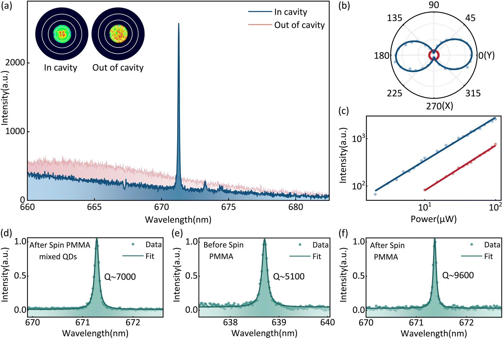 | ||
| Fig. 3 Characterization of the enhanced PL spectrum and the cavity mode. (a) The comparison of the PL spectrum from CdSe/ZnS QDs in (blue) and out of the BIC-based cavity (red), shows an 8.5-fold PL intensity enhancement. The insets show the far-field radiation patterns for QDs in and out of the cavity. The white concentric circles correspond to θ = 10°, 20°, 30° from the inner one to the outer one, respectively. (b) The linear and isotropic polarization characteristics of the PL signal from CdSe/ZnS QDs in (blue) and out of the BIC-based cavity (red). (c) PL intensities dependence on the excitation power for the QDs in (blue) and out of the BIC-based cavity (red). (d) Measured PL spectrum for the cavity mode after spin-coating PMMA mixed CdSe/ZnS QDs (Q ≈ 7000), (e) before spin-coating PMMA (Q ≈ 5100) and (f) after spin-coating PMMA (Q ≈ 9600). The results indicate that the Q-factor of the cavity mode can be significantly boosted with PMMA coating which provides a symmetric refractive index distribution along the vertical direction. | ||
2.4 Accelerated decay rate
The spontaneous emission enhancement of QDs caused by their coupling with high density-of-states modes is typically accompanied by a faster radiation rate. In order to quantitatively characterize the spontaneous emission enhancement assisted by the BIC-based cavity, we performed measured PL lifetimes using pico-second pulses. Fig. 4 shows the normalized time-resolved PL spectra from CdSe/ZnS QDs in and out of the BIC-based cavity. For the QDs out of the BIC-based cavity, the decay follows a single-exponential function: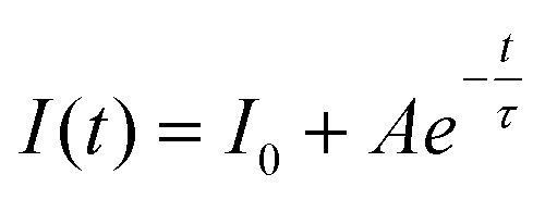 | (1) |
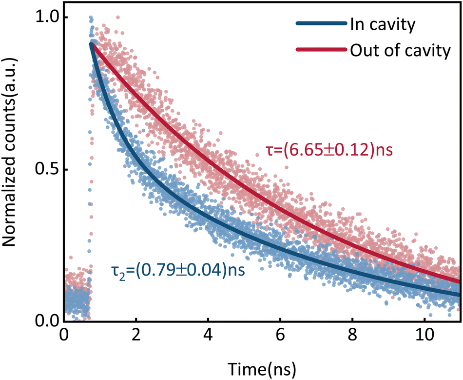 | ||
| Fig. 4 The normalized time-resolved PL spectra from CdSe/ZnS QDs in (blue) and out of (red), the BIC-based cavity. The dots show the raw experimental data. A Purcell factor of 8.4 was obtained by taking the ratio between the lifetimes of τ2 and τ. | ||
The fitting curves gave the measured lifetime τ = 6.65 ns. Such a PL lifetime is close to those reported previously.41 In contrast, the PL decay for the CdSe/ZnS QDs in the BIC-based cavity, nearly followed a double-exponential function:
 | (2) |
The double-exponential function fitting gave a slow lifetime of τ1 = 6.77 ns similar to τ1 = 6.65 ns in the uncoupled case with amplitude A1 = 0.71 and a fast lifetime of τ2 = 0.79 ns related to the strong coupled process with amplitude A2 = 0.86. The amplitude A2 is slightly larger than A1 indicating that more than half of the QDs in the focusing spot are effectively coupled to the cavity. The spontaneous emission enhancement of 8.4 can be obtained by calculating the ratio of the QDs lifetime in the cavity and out of the cavity, namely τ/τ2, which quantifies the change of the QD decay dynamics in the BIC cavity.42 Both the intensity enhancement and the lifetime reduction suggest that efficient coupling between the CdSe/ZnS QDs and the SiN PhC was achieved in our device.
3 Conclusions
In summary, we have demonstrated a compact and high-performance integrated light emitter based on the combination of the BIC-based SiN PhC cavity and active medium of CdSe/ZnS dots. Under the lateral confinement of the boundary band-gap PhC structure and the environment of symmetric refractive index distribution provided by the encapsulated PMMA, our cavity with a size smaller than 10 μm × 10 μm, possesses a high Q-factor of 7000 for a miniaturized BIC resonant mode. Such a high-Q cavity provides a platform for strong interaction between optical fields and the ultra-thin PMMA films with low concentration of CdSe/ZnS QDs, rendering enhancement of PL intensity with a factor of 8.5 and reduction of QDs lifetime with a factor of 8.4. The PL enhancement of the CdSe/ZnS QDs in the surface-emitting cavity provides the possibility of controlling spontaneous emissions for single-photon emissions. Our design provides a way to integrate colloidal QDs onto integrated photonic devices, and further develop hybrid large-scale photonic integrated circuits for applications in integrated quantum photonics.Author contributions
Z. J. L. and J. L. conceptualised the work. G. X. Q. carried out the measurements. G. X. Q. and D. Z. W. analysed the data. Z. J. L. and G. X. Q. drafted the manuscript and all authors contributed to the final draft. Z. J. L. acquired funding and supervised the project.Conflicts of interest
There are no conflicts to declare.Acknowledgements
This project is supported by the National Natural Science Foundation of China (Grant No. 12204019), the National Postdoctoral Program for Innovative Talents (Grant No. BX20220010) and the China Postdoctoral Science Foundation (Grant No. 2022M710233). D. Z. W. is supported by the Fundamental Research Funds for the Central Universities, Sun Yat-sen University (Grant No. 22lgqb32).References
- M. A. Hines and P. Guyot-Sionnest, J. Phys. Chem., 1996, 100, 468–471 CrossRef CAS
.
- S. Baskoutas and A. F. Terzis, J. Appl. Phys., 2006, 99, 013708 CrossRef
- J. Caruge, J. E. Halpert, V. Wood, V. Bulović and M. Bawendi, Nat. Photonics, 2008, 2, 247–250 CrossRef CAS
- Q. Sun, Y. A. Wang, L. S. Li, D. Wang, T. Zhu, J. Xu, C. Yang and Y. Li, Nat. Photonics, 2007, 1, 717–722 CrossRef CAS
- Y. Shirasaki, G. J. Supran, M. G. Bawendi and V. Bulović, Nat. Photonics, 2013, 7, 13–23 CrossRef CAS
- Y.-S. Park, J. Roh, B. T. Diroll, R. D. Schaller and V. I. Klimov, Nat. Rev. Mater., 2021, 6, 382–401 CrossRef CAS
- C. Gollner, J. Ziegler, L. Protesescu, D. N. Dirin, R. T. Lechner, G. Fritz-Popovski, M. Sytnyk, S. Yakunin, S. Rotter and A. A. Yousefi Amin,
et al.
, ACS Nano, 2015, 9, 9792–9801 CrossRef CAS PubMed
- B. Min, S. Kim, K. Okamoto, L. Yang, A. Scherer, H. Atwater and K. Vahala, Appl. Phys. Lett., 2006, 89, 191124 CrossRef
- Y. Wang, V. D. Ta, K. S. Leck, B. H. I. Tan, Z. Wang, T. He, C.-D. Ohl, H. V. Demir and H. Sun, Nano Lett., 2017, 17, 2640–2646 CrossRef CAS PubMed
- B. le Feber, F. Prins, E. De Leo, F. T. Rabouw and D. J. Norris, Nano Lett., 2018, 18, 1028–1034 CrossRef CAS PubMed
- W. Xie, T. Stöferle, G. Raino, T. Aubert, S. Bisschop, Y. Zhu, R. F. Mahrt, P. Geiregat, E. Brainis and Z. Hens,
et al.
, Adv. Mater., 2017, 29, 1604866 CrossRef PubMed
- M. Kahl, T. Thomay, V. Kohnle, K. Beha, J. Merlein, M. Hagner, A. Halm, J. Ziegler, T. Nann and Y. Fedutik,
et al.
, Nano Lett., 2007, 7, 2897–2900 CrossRef CAS PubMed
- B. Liu, Q. Wu, Z. Zhu, C. Cheng, M. Gu, J. Xu, H. Chen, J. Liu, L. Chen and Z. Zhang,
et al.
, Appl. Phys. Lett., 2017, 111, 081904 CrossRef
- V. Reboud, N. Kehagias, M. Zelsmann, M. Striccoli, M. Tamborra, M. Curri, A. Agostiano, D. Mecerreyes, J. Alduncin and C. S. Torres, Microelectron. Eng., 2007, 84, 1574–1577 CrossRef CAS
- X. Yuan, L. Shi, Q. Wang, C. Chen, X. Liu, L. Sun, B. Zhang, J. Zi and W. Lu, Opt. Express, 2014, 22, 23473–23479 CrossRef CAS PubMed
- O. Kulakovich, N. Strekal, A. Yaroshevich, S. Maskevich, S. Gaponenko, I. Nabiev, U. Woggon and M. Artemyev, Nano Lett., 2002, 2, 1449–1452 CrossRef CAS
- J.-H. Song, T. Atay, S. Shi, H. Urabe and A. V. Nurmikko, Nano Lett., 2005, 5, 1557–1561 CrossRef CAS PubMed
- C. W. Hsu, B. Zhen, A. D. Stone, J. D. Joannopoulos and M. Soljačić, Nat. Rev. Mater., 2016, 1, 1–13 Search PubMed
- Y. Yang, C. Peng, Y. Liang, Z. Li and S. Noda, Phys. Rev. Lett., 2014, 113, 037401 CrossRef PubMed
- J. Jin, X. Yin, L. Ni, M. Soljačić, B. Zhen and C. Peng, Nature, 2019, 574, 501–504 CrossRef CAS PubMed
- K. Koshelev, A. Bogdanov and Y. Kivshar, Sci. Bull., 2019, 64, 836–842 CrossRef PubMed
- F. Wu, J. Wu, Z. Guo, H. Jiang, Y. Sun, Y. Li, J. Ren and H. Chen, Phys. Rev. Appl., 2019, 12, 014028 CrossRef CAS
- Y. Akahane, T. Asano, B.-S. Song and S. Noda, Nature, 2003, 425, 944–947 CrossRef CAS PubMed
- S. Noda, A. Chutinan and M. Imada, Nature, 2000, 407, 608–610 CrossRef CAS PubMed
- A. Leitis, A. Tittl, M. Liu, B. H. Lee, M. B. Gu, Y. S. Kivshar and H. Altug, Sci. Adv., 2019, 5, eaaw2871 CrossRef PubMed
- F. Yesilkoy, E. R. Arvelo, Y. Jahani, M. Liu, A. Tittl, V. Cevher, Y. Kivshar and H. Altug, Nat. Photonics, 2019, 13, 390–396 CrossRef CAS
- C. Huang, C. Zhang, S. Xiao, Y. Wang, Y. Fan, Y. Liu, N. Zhang, G. Qu, H. Ji and J. Han,
et al.
, Science, 2020, 367, 1018–1021 CrossRef CAS PubMed
- M.-S. Hwang, H.-C. Lee, K.-H. Kim, K.-Y. Jeong, S.-H. Kwon, K. Koshelev, Y. Kivshar and H.-G. Park, Nat. Commun., 2021, 12, 1–9 CrossRef PubMed
- S. S. Kruk, L. Wang, B. Sain, Z. Dong, J. Yang, T. Zentgraf and Y. Kivshar, Nat. Photonics, 2022, 16, 561–565 CrossRef CAS
- Z. Liu, J. Wang, B. Chen, Y. Wei, W. Liu and J. Liu, Nano Lett., 2021, 21, 7405–7410 CrossRef CAS PubMed
- J. Wang, Z. Liu, J. Xiang, B. Chen, Y. Wei, W. Liu, Y. Xu, S. Lan and J. Liu, Nanophotonics, 2021, 10, 4273–4278 CrossRef CAS
- Z. Liu, Y. Xu, Y. Lin, J. Xiang, T. Feng, Q. Cao, J. Li, S. Lan and J. Liu, Phys. Rev. Lett., 2019, 123, 253901 CrossRef CAS PubMed
- K. Min, S. Choi, Y. Choi and H. Jeon, Nanoscale, 2014, 6, 14531–14537 RSC
- S. Chen, K. Roh, J. Lee, W. K. Chong, Y. Lu, N. Mathews, T. C. Sum and A. Nurmikko, ACS Nano, 2016, 10, 3959–3967 CrossRef CAS PubMed
- X. Ge, M. Minkov, S. Fan, X. Li and W. Zhou, npj 2D Mater. Appl., 2019, 3, 1–5 CrossRef CAS
- J. Wang, M. Clementi, M. Minkov, A. Barone, J.-F. Carlin, N. Grandjean, D. Gerace, S. Fan, M. Galli and R. Houdré, Optica, 2020, 7, 1126–1132 CrossRef CAS
- Z. He, B. Chen, Y. Hua, Z. Liu, Y. Wei, S. Liu, A. Hu, X. Shen, Y. Zhang and Y. Gao,
et al.
, Adv. Opt. Mater., 2020, 8, 2000453 CrossRef CAS
- C. F. Fong, Y. Yin, Y. Chen, D. Rosser, J. Xing, A. Majumdar and Q. Xiong, Opt. Express, 2019, 27, 18673–18682 CrossRef CAS PubMed
-
J. Liu, F. Bo, L. Chang, C.-H. Dong, X. Ou, B. Regan, X. Shen, Q. Song, B. Yao and W. Zhang, et al., Science China Physics, Mechanics & Astronomy, 2022, vol. 65, pp. 1–19 Search PubMed
- Z. Chen, X. Yin, J. Jin, Z. Zheng, Z. Zhang, F. Wang, L. He, B. Zhen and C. Peng, Sci. Bull., 2022, 67, 359–366 CrossRef PubMed
- S. Chandra, J. Doran, S. McCormack, M. Kennedy and A. Chatten, Sol. Energy Mater. Sol. Cells, 2012, 98, 385–390 CrossRef CAS
- B. Chen, Z. He, Z.-J. Liu, Y.-K. Wang, Y.-N. Gao, I. Aharonovich, Z.-Q. Xu and J. Liu, Nanophotonics, 2020, 9, 2587–2592 CAS
- Y.-W. Lu, J.-F. Liu, Z. Liao and X.-H. Wang, Sci. China Phys. Mech. Astron., 2021, 64, 274212 CrossRef CAS
Footnote |
| † These authors contributed equally to this work. |
| This journal is © The Royal Society of Chemistry 2023 |