
Coherent imaging and dynamics of excitons in MoSe2 monolayers epitaxially grown on hexagonal boron nitride†
Karolina Ewa
Połczyńska
*a,
Simon
Le Denmat
b,
Takashi
Taniguchi
c,
Kenji
Watanabe
 c,
Marek
Potemski
ade,
Piotr
Kossacki
a,
Wojciech
Pacuski
a and
Jacek
Kasprzak
*abf
c,
Marek
Potemski
ade,
Piotr
Kossacki
a,
Wojciech
Pacuski
a and
Jacek
Kasprzak
*abf
aFaculty of Physics, University of Warsaw, ul. Pasteura 5, 02-093 Warszawa, Poland. E-mail: karolina.polczynska@fuw.edu.pl
bUniv. Grenoble Alpes, CNRS, Grenoble INP, Institut Néel, 25 rue des Martyrs, 38000 Grenoble, France
cInternational Center for Materials Nanoarchitectonics, National Institute for Materials Science, 1-1 Namiki, Tsukuba 305-0044, Japan
dLaboratoire National des Champs Magnétiques Intenses, CNRS-UGA-UPS-INSA-EMFL, 25 Av. des Martyrs, 38042 Grenoble, France
eCENTERA Labs, Institute of High Pressure Physics, PAS, PL-01-142 Warsaw, Poland
fWalter Schottky Institut and TUM School of Natural Sciences, Technische Universität München, 85748 Garching, Germany
First published on 21st March 2023
Abstract
Using four-wave mixing microscopy, we measure the coherent response and ultrafast dynamics of excitons and trions in MoSe2 monolayers grown by molecular beam epitaxy on thin films of hexagonal boron nitride. We assess inhomogeneous and homogeneous broadenings in the transition spectral lineshape. The impact of phonons on the homogeneous dephasing is inferred via the temperature dependence of the dephasing. Four-wave mixing mapping, combined with atomic force microscopy, reveals spatial correlations between exciton oscillator strength, inhomogeneous broadening and the sample morphology. The quality of the coherent optical response of epitaxially grown transition metal dichalcogenides now becomes comparable to the samples produced by mechanical exfoliation, enabling the coherent nonlinear spectroscopy of innovative materials, like magnetic layers or Janus semiconductors.
1 Introduction
We are witnessing astonishing progress in the assembly of complex heterostructures based on the monolayers of semiconducting transition metal dichalcogenides (TMDs), an iconic example being MoSe2 placed between the flakes of hexagonal boron nitride (hBN). The fabrication technology principally relies on the mechanical exfoliation of thin films from van der Waals bulk crystals, similarly to the revolutionary extraction of graphene from graphite.1 This technique has enabled important discoveries in the field of condensed matter physics to name a few: demonstrations of novel strongly-correlated electron systems,2 moiré quantum matter,3 optical sensing of a quantum Hall effect,4 non-hydrogenic Rydberg series of excitonic excitations,5 high-harmonic optical generation6,7 and giant coherent nonlinear responses.8,9 It also boosted developments toward the future applications of these materials in optoelectronics10 and medicine.11 While the non-scalability of the exfoliation top-down approach is not an issue for the fundamental research, for which the proof-of-principle demonstrations are essential, it is a major roadblock on the academia–industry pathway of this field. In order to merge these novel materials with semiconductor microelectronics, strain-free monolayer samples homogeneously covering wafers of a few cm in diameter are required.12This can only be achieved by employing epitaxial techniques. The chemical vapor deposition of TMD layers, including monolayers, has been reported13 with post-growth processing improving the samples’ quality.14 Also molecular beam epitaxy of TMDs has been highlighted.15,16 The optical response of the as-grown monolayers was dominated by the inhomogeneous broadening of the studied exciton transitions (EX), typically in a range of several tens meV. Moreover, the MBE growth of the materials incorporating transition metals, such as Mo and W, is particularly challenging owing to their low surface mobility. This causes their aggregation, especially when roaming on a rough surface, such that typically grains not exceeding 10 nm size were obtained on a commonly used SiO2 substrate. On top of that, epitaxy has a slow rate and requires high temperatures for sublimation, rendering it demanding. Recently, a breakthrough in this area has been achieved:17 using atomically flat and thin hBN layers, MoSe2 monolayers with 85% of surface coverage were MBE-grown, homogenously occupying terraces of several hundreds of μm. A step-like improvement of the optical response was achieved with exciton's photoluminescence line width below 10 meV and a suppressed distribution of the central transition energy, down to 0.16 meV. Importantly, good optical properties of the MBE-grown TMD are achieved without post-growth mechanical processing. Further to that, a heteroepitaxial growth of MoSe2 monolayers on hBN, yielding wafer-scale van der Waals heterostructures of a good optical quality, has recently been reported.12
For optoelectronic applications, like ultrafast photodetectors, it is important to examine the nonlinear absorption properties of these materials. In this work, we investigate the coherent optical response of these high quality epitaxial MoSe2 monolayers using tools of nonlinear spectroscopy. By performing four-wave mixing (FWM) microscopy,18 we assess the exciton's and trion's inhomogeneous σ and homogeneous γ line widths (FWHM). The impact of phonons on γ is evaluated by performing temperature dependence studies of the dephasing. Using FWM, we also measure the exciton density dynamics and find a longer population lifetime of trions with respect to excitons, as predicted in the literature.19,20 Next, by performing FWM spatial imaging we observe correlations between the FWM amplitude and σ.
2 Optical characterization
A large scale atomic force microscopy (AFM) image of the investigated sample is presented in Fig. 1a. We concentrate on the macroscopic hBN flake, containing atomically flat terraces on several micron scale, which is deposited onto a SiO2/Si substrate. The corresponding AFM image, measured with enhanced spatial resolution, is shown in Fig. 1b. Therein, we recognize MoSe2 monolayers with a typical size of around 100 nm, homogeneously covering the hBN flake, not yet affected by the grain coalescence process, required to obtain a complete monolayer.17 Further AFM images are presented in ESI Fig. S1.† The fabrication technology is described in ref. 17. The sample presented in this work has been prepared in the following process: before commencing the MBE-growth, the substrate containing hBN flakes was degassed for 10 min at 750 °C. Next, during 25 minutes of growth, we deposited a single monolayer of MoSe2 at 300 °C, and finally, we annealed the sample in Se flux for 2 h at 750 °C. Se was deposited from a standard effusion cell and Mo was deposited from the e-beam source with a Mo rod heated at one end by electrons. After the growth, there was no need for further processing of the sample to perform optical measurements.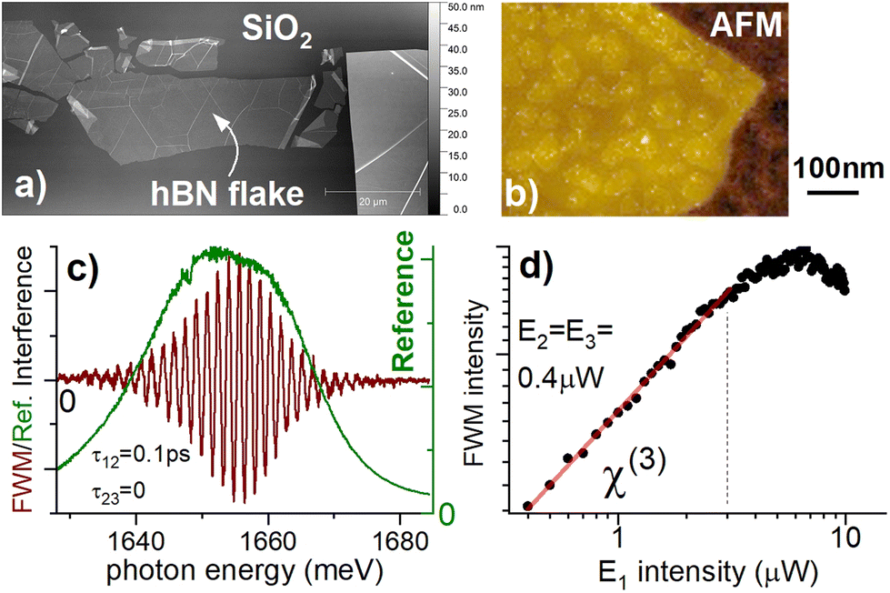 | ||
| Fig. 1 Optical and structural characterization of the MBE-grown MoSe2 monolayer. (a) A large scale atomic force microscopy (AFM) image of the sample, showing the hBN flake on top of the SiO2 substrate. (b) The morphology of the sample revealed by AFM performed with enhanced spatial resolution. The MoSe2 monolayer flakes with a typical size of 100 nm grow on atomically flat terraces of hBN. (c) Four-wave mixing spectral interferogram (in red) measured at the exciton energy at T = 5 K. The excitation pulse is given in green. (d) Four-wave mixing intensity dependence. The linear regime of FWM, also known as the χ(3) regime, occurs for the driving powers up to 3 μW. Upon increasing the excitation intensity, the onset of Rabi rotation is visible. | ||
The optical experiments were performed at T = 5 K, unless stated otherwise. In the photoluminescence study, presented in ESI Fig. S2,† we observed the narrow emission lines of neutral excitons and charged excitons (trions), similarly to that in ref. 17. The same exciton complexes are distinguished in white light reflectance. To infer the coherent response of these monolayers we perform FWM microscopy. We employ the same configuration of the setup as in ref. 9 and 21. On the sample surface, we focus three, colinearly polarized 100 fs pulses  generated by a Ti:sapphire laser.
  are spectrally centered at 750 nm, which is the expected wavelength of the exciton transition in MoSe2 monolayers. Using acousto-optic deflectors operating at around 80 MHz, we introduce distinct phase drifts (ϕ1, ϕ2, ϕ3) within each of the triple-pulse sequences of the pulse train. In the reflected light, one can still differentiate and recover the amplitude and the phase of the pulses by homodyning and performing spectral interferometry with a reference pulse
  . Conversely, various nonlinear signals propagate at yet another frequencies within the reflected pulse train sequence. In particular, the FWM which is proportional to
 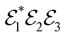 has a precisely defined phase ϕFWM = ϕ3 + ϕ2 − ϕ1, which we detect by optical heterodyning. The resulting spectral interference of such heterodyned FWM with the
  is presented in Fig. 1c. An example of the FWM spectrum, retrieved from the interferogram via spectral interferometry, is shown in ESI Fig. S2c.† The signal-to-noise ratio is similar to previously studied bare monolayers obtained via mechanical exfoliation.9 To remind, by measuring the FWM integrated amplitude as a function of the delay τ12 (τ23) between the first (last) two arriving pulses, the dynamics of the excitonic coherence (density) is monitored—the relevant pulse sequences employed in our experiments are depicted at the top of Fig. 2 and 3, respectively.
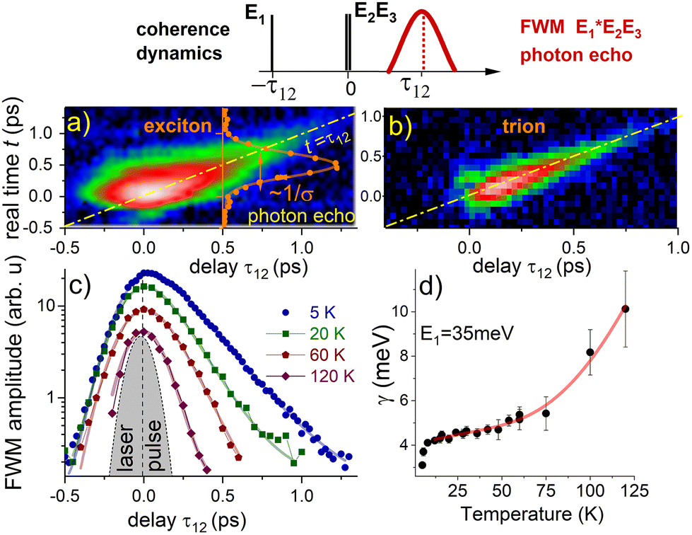 | ||
| Fig. 2 Analysis of dephasing via four-wave mixing. Top: the pulse sequence employed to probe the coherence dynamics. (a) Time-resolved four-wave mixing as a function of delay τ12 measured at the exciton transition displaying the photon echo. The temporal width of the echo yields the inhomogeneous broadening σEX = 11.8 meV. (b) as (a) but measured at the trion transition. The pronounced echo yields σTR = 30.4 meV. (c) Exciton dephasing versus temperature as indicated, measured via time-integrated FWM. (d) Resulting exciton homogeneous line width versus temperature. The red trace is the fit corresponding to a linear increase of γ due to interaction with acoustic phonons, followed by an exponential increase owing to the thermal activation of the optical phonons. | ||
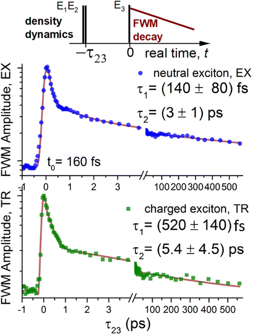 | ||
| Fig. 3 Exciton and trion density dynamics measured via four-wave mixing. Top: a pulse sequence used to measure the density grating evolution via FWM, middle (and bottom): exciton (and trion) density dynamics showing a biexponential decay. | ||
At first, we take care to perform the experiments in the χ(3) regime, in order to minimize excitation induced dephasing21 and local field effects. To check that, we carry out the FWM intensity dependence measurement,22 presented in Fig. 1d. We observe a purely linear increase of the FWM when increasing the  average power up to around 3 μW, followed by the saturation and the onset of the local-field induced Rabi rotation. The following experiments have been therefore performed for
  .
.
3 Coherence dynamics
The main advantage of FWM spectroscopy is its capability to accurately measure homogeneous, γ, and inhomogeneous, σ, contributions to the spectral line shape of the optical transition. By construction, there is a phase conjugation between the first order absorption induced by and the FWM signal. In the presence of σ, such conjugation generates the rephasing and constructive interference in the FWM transient, known as photon echo, similar to the spin-echo phenomenon in nuclear magnetic resonance spectroscopy. From the decay of the echo as a function of τ12 one can measure the intrinsic dephasing time T2 of the optical transition in the material and the homogeneous broadening (FWHM) γ = 2ħ/T2, whereas the temporal width of the echo yields σ.
We now thus analyse the exciton's spectral lineshape. The time-resolved FWM signal of the exciton is shown in Fig. 2a. We observe the formation of a photon-echo: with increasing the delay τ12, the maximum of the FWM transient shifts towards longer times t, such that the signal is aligned along the diagonal t = τ12 in the two-dimensional representation. The presence of σ, which quantifies the amount of electronic disorder, induces rephasing in the FWM transient, generating its Gaussian form, as depicted in orange. From the temporal FWHM of this Gaussian equal to δt = 363 fs (corrected with respect to the pulse duration), we can calculate the spectral inhomogeneous broadening FWHM to be σEX = 8![[thin space (1/6-em)]](https://www.rsc.org/images/entities/char_2009.gif) ln(2)ħ/δt = 11.8 meV. This value is consistent with the line width read from the FWM spectral interferogram, shown in Fig. 1c.
ln(2)ħ/δt = 11.8 meV. This value is consistent with the line width read from the FWM spectral interferogram, shown in Fig. 1c.
Importantly, when the photon echo is developed, the time-integrated (TI) FWM amplitude as a function of τ12 is not sensitive to σ, but instead reflects the microscopic dephasing time T2, governing the FWHM of the homogeneous broadening γ = 2ħ/T2. The blue circles in Fig. 2c show such time-integrated FWM at T = 5 K. It is fitted with the exponential decay convoluted with the Gaussian, to account for a finite pulse duration, as represented in grey. For τ12 > 0, an exponential decay is observed, yielding γEX (5 K) = 3 meV. This value is three times that measured on the bare MoSe2 MLs9 and is also larger than that in hBN/MoSe2/hBN heterostructures (produced via exfoliation and deterministic transfer methods) operating at the homogeneous limit.21 We attribute such a rapid loss of the exciton coherence to the strong non-radiative processes in our MBE grown samples. Interestingly, we also observe the signal for τ12 < 0: the FWM onset is detected noticeably earlier than expected from the finite pulse duration, especially bearing in mind a careful compensation of the temporal chirp in our experiments. From the exponential decay toward negative delays, we determine the coherence time due to the local field effect of approximately TLC = 0.1 ps.
In Fig. 2b, we present analogous time-resolved FWM, but this time measured on the trion transition. We remark that the photon echo is even more pronounced, i.e. the FWM is yet more congregated along the diagonal, indicating a larger σ. Indeed, we here determine σTR = 30.4 meV. Again, from the TI FWM (not shown) we determine γTR = (7.7 ± 0.2) meV. This larger value with respect to γEX is expected and consistent with recent measurements on exfoliated MoSe29 and past predictions and experiments on GaAs QWs.19 We further notice lack of the signal for τ12 < 0 ps, due to a larger σ.
In Fig. 2d we report the temperature dependence of γEX. We observe a linear increase of γ, due to a coupling with acoustic phonons. It is then followed by an exponential growth with an activation energy of 35 meV, well corresponding to the thermal activation of optical phonons.9,22 This phonon induced dephasing is therefore similar to previously reported TMDs and prior measurements on GaAs quantum wells. With increasing temperature, we have to deal not only with the increased dephasing rate, but also with a dramatic suppression of the FWM signal amplitude, such that we are unable to retrieve T2 above 130 K.
4 Population dynamics
We now move to the pulse sequence depicted in Fig. 3 (top): the first two beams generate a temporal density grating in a material, which is then converted into a FWM signal by the last arriving beam. In this sequence, we thus probe the dynamics of excitons resonantly injected into the light cone. The result is presented in Fig. 3. As in recent works,23–25 the data are modeled as a coherent superposition of several complex exponential decays. In our case, two processes are sufficient to describe the observed dynamics: the initial ultrafast decay is followed by a longer component. The first component is due to both radiative decay and non-radiative exciton scattering out of the light cone, the second component describes the effective secondary scattering of dark excitons back into the light cone. The trion's radiative lifetime is expected to be significantly longer than the exciton's one, as was also measured experimentally.25 Here instead, the first fast decay component for the trion is barely τ1,TR = 0.52 ps, therefore indicating a prominent non-radiative decay channel. An ultrafast initial decay of the neutral exciton τ1,EX = 0.14 ps, at the limit of the temporal resolution of the experiment, also points toward the existence of a fast non-radiative recombination channel.5 Coherent imaging and correlations
In this last section, we discuss the coherent spatial imaging of the sample. The time-integrated FWM map spanning across a large area of (36 × 72) μm2 is shown in Fig. 4a. Let us remind that MoSe2 covers the entire sample. We however observed that the coherent response is uniquely generated at the hBN flakes. We also distinguished a decreased FWM signal along the discontinuities in the hBN flake and found virtually no signal from the material deposited on the SiO2 substrate. Furthermore, we noticed that no FWM is generated at the thick hBN flakes, with increased roughness and no well-defined atomic terraces. The presence of the atomically flat surface, as provided by thin hBN flakes, is therefore required to perform a successful epitaxy and to carry out coherence spectroscopy reported here. The hyperspectral imaging allows us to determine the central energy of the FWM spectrum. We find that the exciton peak position is centered at 1652.5 meV and is remarkably homogeneous with a standard deviation (FWHM) of 0.87 meV across the entire flake.17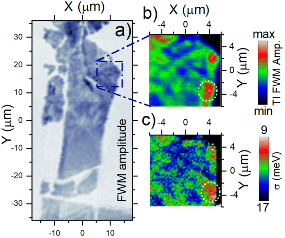 | ||
| Fig. 4 Four-wave mixing imaging characteristics. (a) Time-integrated FWM amplitude measured on a large area of (36 × 72) μm2 showing the strong signal generated at MoSe2 monolayers grown on hBN. (b) as (a), but zoomed in, as indicated by the blue square. (c) Spatial mapping of the spectral inhomogeneous broadening (FWHM) obtained from the temporal width of the photon echo. Areas generating a strong FWM in (b) also display the lowest inhomogeneous broadening in (c), as indicated by the yellow circle. | ||
We carry on by recording a high resolution FWM image (employing a raster scanning step size of 0.2 μm), around the spot at which the temporal dynamics was measured. In Fig. 4b we notice a strong variation of the FWM signal's amplitude. Having access to time-resolved FWM, we can map out σ, and plot it in Fig. 4c. In agreement with recent studies,24,26 we find correlations between the FWM amplitude, linked with the transition oscillator strength, and σ, reflecting the disorder: a stronger FWM signal is detected at the areas with a lower inhomogeneous broadening, as marked with yellow circles. Similar correlations were also found on neighbouring hBN flakes on the same sample, further supporting our claim, see ESI Fig. S3.† Other correlations, between the FWM amplitude and parameters provided by the AFM measurements (height of the hBN terraces, spatial density and orientation of the monolayers) were not detected. However, a decrease of the FWM signal is observed along the hBN cracks.
6 Conclusions & outlook
We have demonstrated a robust coherent nonlinear optical response of MBE-grown MoSe2 monolayers. By exploiting FWM signals in the temporal domain we have measured dephasing of exciton complexes and ascertained their dephasing via temperature dependence studies. Our results show that these epitaxial monolayers, which could be compatible with the semiconductor optoelectronics industry if grown on wafer-size epitaxial hBN, already display an excellent optical response. This however is promoted by their crystallisation on atomically flat surfaces, here provided by exfoliated hBN flakes. The quality and intensity of their coherent nonlinear optical response is comparable to their non-encapsulated counterparts obtained via exfoliation.The versatility of MBE growth opens new research avenues for these materials. For example, Janus architecture27 or MoXW1−XSe2 alloys with a well-controlled stoichiometry can be fabricated. Such a technology could be employed to grow magnetic two-dimensional materials, like CrSBr. By exploiting a strong spin–orbit interaction in TMD monolayers, with controlled doping (for example with vanadium atoms), one can obtain a ferromagnetic semiconductor operating at room temperature.28–30 These layers could also be embedded into microcavities and serve as excitonic work-benches in polaritonics. Furthermore, with lateral structurization one could introduce in-plane confinement and manufacture quantum dots or quantum wires, permitting one to explore the physics of edge states.
Surprisingly, epitaxial growth via CVD has recently been employed to understand the surface reconstruction mechanisms during the formation of moiré quantum matter.31,32 In this context, we believe that combining the MBE-growth of transition metal dichalcogenides, homo- and hetero-bilayers with nonlinear spectroscopy could yield relevant findings within the crossover of material science at the nanoscale and their light–matter interaction.
Author contributions
The epitaxial growth of MoSe2 samples was performed by K. P. and W. P. The hBN crystals were grown by T. T. and K. W. The AFM imaging was carried out by S. L-D. The spectroscopy and data analysis were performed by J. K. and K. P. The project was initiated and supervised by P. K., M. P. and W. P. The paper was written by J. K. and W. P. All authors discussed the results and commented on the manuscript.Conflicts of interest
There are no conflicts to declare.Acknowledgements
We gratefully acknowledge the financial support from project no. 2020/39/B/ST3/03251 and 2021/41/B/ST3/04183 financed by the National Science Centre (Poland), “Tandem for Excellence” IDUB scheme at the University of Warsaw and EU Graphene Flagship. J. K. acknowledges the support of TU Munich through the Global Invited Professorship Program 2021–2023. M. P. acknowledges support from the Foundation for Polish Science (MAB/2018/9 Grant within the IRA Program financed by EU within the SG OP Program). K. W. and T. T. acknowledge support from the Elemental Strategy Initiative conducted by the MEXT, Japan, (grant no. JPMXP0112101001), JSPS KAKENHI (grant no. JP20H00354), and the CREST (JPMJCR15F3), JST. We thank Daniel Wigger for his comments on the manuscript.References
- K. S. Novoselov, A. K. Geim, S. V. Morozov, D. Jiang, Y. Zhang, S. V. Dubnosi, I. V. Grigorieva and A. A. Firsov, Science, 2004, 306, 666–669 CrossRef CAS PubMed.
- T. Smoleński, P. E. Dolgirev, C. Kuhlenkamp, A. Popert, Y. Shimazaki, P. Back, X. Lu, M. Kroner, K. Watanabe, T. Taniguchi, I. Esterlis, E. Demler and A. Imamoğlu, Nature, 2021, 595, 53–57 CrossRef PubMed.
- D. Huang, J. Choi, C.-K. Shih and X. Li, Nat. Nanotechnol., 2022, 17, 227–238 CrossRef CAS PubMed.
- A. Popert, Y. Shimazaki, M. Kroner, K. Watanabe, T. Taniguchi, A. Imamoğlu and T. Smoleński, Nano Lett., 2022, 22, 7363–7369 CrossRef CAS PubMed.
- A. Chernikov, T. C. Berkelbach, H. M. Hill, A. Rigosi, Y. Li, O. B. Aslan, D. R. Reichman, M. S. Hybertsen and T. F. Heinz, Phys. Rev. Lett., 2014, 113, 076802 CrossRef CAS PubMed.
- A. Säynätjoki, L. Karvonen, H. Rostami, A. Autere, S. Mehravar, A. Lombardo, R. A. Norwood, T. Hasan, N. Peyghambarian, H. Lipsanen, K. Kieu, A. C. Ferrari, M. Polini and Z. Sun, Nat. Commun., 2017, 8, 893 CrossRef PubMed.
- H. Liu, Y. Li, Y. S. You, S. Ghimire, T. F. Heinz and D. A. Reis, Nat. Phys., 2017, 13, 262–265 Search PubMed.
- G. Moody, C. K. Dass, K. Hao, C.-H. Chen, L.-J. Li, A. Singh, K. Tran, G. Clark, X. Xu, G. Berghäuser, E. Malic, A. Knorr and X. Li, Nat. Commun., 2015, 6, 8315 Search PubMed.
- T. Jakubczyk, V. Delmonte, M. Koperski, K. Nogajewski, C. Faugeras, W. Langbein, M. Potemski and J. Kasprzak, Nano Lett., 2016, 16, 5333–5339 CrossRef CAS PubMed.
- F. H. L. Koppens, T. Mueller, P. Avouris, A. C. Ferrari, M. S. Vitiello and M. Polini, Nat. Nanotechnol., 2014, 9, 780–793 CrossRef CAS PubMed.
- D. Kalita, V. Bouchiat, L. Marty and N. Bendiab, US Pat.11040191, 2021 Search PubMed.
- K. Ludwiczak, A. K. Dabrowska, J. Binder, M. Tokarczyk, J. Iwański, B. Kurowska, J. Turczyńki, G. Kowalski, R. Bożek, R. StÈ©pniewski, W. Pacuski and A. Wysmołek, ACS Appl. Mater. Interfaces, 2021, 13, 47904–47911 CrossRef CAS PubMed.
- X. Wang, Y. Gong, G. Shi, W. L. Chow, K. Keyshar, G. Ye, R. Vajtai, J. Lou, Z. Liu, E. Ringe, B. K. Tay and P. M. Ajayan, ACS Nano, 2014, 8, 5125–5131 CrossRef CAS PubMed.
- S. Shree, A. George, T. Lehnert, C. Neumann, M. Benelajla, C. Robert, X. Marie, K. Watanabe, T. Taniguchi, U. Kaiser, B. Urbaszek and A. Turchanin, 2D Mater., 2019, 7, 015011 CrossRef.
- M.-W. Chen, D. Ovchinnikov, S. Lazar, M. Pizzochero, M. B. Whitwick, A. Surrente, M. Baranowski, O. L. Sanchez, P. Gillet, P. Płochocka, O. V. Yazyev and A. Kis, ACS Nano, 2017, 11, 6355–6361 CrossRef CAS PubMed.
- C. Vergnaud, M. Gay, C. Alvarez, M.-T. Dau, F. Pierre, D. Jalabert, C. Licitra, A. Marty, C. Beigné, B. Grévin, O. Renault, H. Okuno and M. Jamet, 2D Mater., 2019, 6, 035019 CrossRef CAS.
- W. Pacuski, M. Grzeszczyk, K. Nogajewski, A. Bogucki, K. Oreszczuk, J. Kucharek, K. E. Połczyńska, B. Seredyński, A. Rodek, R. Bożek, T. Taniguchi, K. Watanabe, S. Kret, J. Sadowski, T. Kazimierczuk, M. Potemski and P. Kossacki, Nano Lett., 2020, 20, 3058–3066 CrossRef CAS PubMed.
- W. Langbein and B. Patton, Opt. Lett., 2006, 31, 1151–1153 CrossRef PubMed.
- A. Esser, E. Runge, R. Zimmermann and W. Langbein, Phys. Rev. B: Condens. Matter Mater. Phys., 2000, 62, 8232–8239 CrossRef CAS.
- F. Rana, O. Koksal, M. Jung, G. Shvets and C. Manolatou, Phys. Rev. B: Condens. Matter Mater. Phys., 2021, 103, 035424 CrossRef CAS.
- C. Boule, D. Vaclavkova, M. Bartos, K. Nogajewski, L. Zdražil, T. Taniguchi, K. Watanabe, M. Potemski and J. Kasprzak, Phys. Rev. Mater., 2020, 4, 034001 CrossRef CAS.
- T. Jakubczyk, K. Nogajewski, M. R. Molas, M. Bartos, W. Langbein, M. Potemski and J. Kasprzak, 2D Mater., 2018, 5, 031007 CrossRef.
- L. Scarpelli, F. Masia, E. M. Alexeev, F. Withers, A. I. Tartakovskii, K. S. Novoselov and W. Langbein, Phys. Rev. B, 2017, 96, 045407 CrossRef.
- T. Jakubczyk, G. Nayak, L. Scarpelli, F. Masia, W.-L. Liu, S. Dubey, N. Bendiab, L. Marty, T. Taniguchi, K. Watanabe, G. N. J. Coraux, V. Bouchiat, W. Langbein, J. Renard and J. Kasprzak, ACS Nano, 2019, 13, 3500–3511 CrossRef CAS PubMed.
- A. J. Rodek, T. Hahn, J. Howarth, T. Taniguchi, K. Watanabe, M. Potemski, P. Kossacki, D. Wigger and J. Kasprzak, 2D Mater., 2023, DOI:10.1088/2053-1583/acc59a.
- T. L. Purz, E. W. Martin, W. G. Holtzmann, P. Rivera, A. Alfrey, K. M. Bates, H. Deng, X. Xu and S. T. Cundiff, J. Chem. Phys., 2022, 156, 214704 CrossRef CAS PubMed.
- M. M. Petrić, M. Kremser, M. Barbone, Y. Qin, Y. Sayyad, Y. Shen, S. Tongay, J. J. Finley, A. R. Botello-Méndez and K. Müller, Phys. Rev. B, 2021, 103, 035414 CrossRef.
- L.-A. T. Nguyen, K. P. Dhakal, Y. Lee, W. Choi, T. D. Nguyen, C. Hong, D. H. Luong, Y.-M. Kim, J. Kim, M. Lee, T. Choi, A. J. Heinrich, J.-H. Kim, D. Lee, D. L. Duong and Y. H. Lee, ACS Nano, 2021, 15, 20267–20277 CrossRef CAS PubMed.
- S. J. Yun, B. W. Cho, T. Dinesh, D. H. Yang, Y. I. Kim, J. W. Jin, S.-H. Yang, T. D. Nguyen, Y.-M. Kim, K. K. Kim, D. L. Duong, S.-G. Kim and Y. H. Lee, Adv. Mater., 2022, 34, 2106551 CrossRef CAS PubMed.
- P. Mallet, F. Chiapello, H. Okuno, H. Boukari, M. Jamet and J.-Y. Veuillen, Phys. Rev. Lett., 2020, 125, 036802 CrossRef CAS PubMed.
- S. Zhao, arXiv, 2022, DOI:10.48550/arXiv.2202.11139.
- Z. Li, arXiv, 2022, DOI:10.48550/arXiv.2212.07686.
Footnote |
| † Electronic supplementary information (ESI) available. See DOI: https://doi.org/10.1039/d2nr04844b |
| This journal is © The Royal Society of Chemistry 2023 |