
 Open Access Article
 This Open Access Article is licensed under a Creative Commons Attribution-Non Commercial 3.0 Unported Licence
AC-driven multicolor electroluminescence from a hybrid WSe2 monolayer/AlGaInP quantum well light-emitting device†
Ya-Hui
Chang
ab,
Yen-Shou
Lin
ab,
Konthoujam
James Singh
 b,
Hsiang-Ting
Lin
a,
Chiao-Yun
Chang
ac,
Zheng-Zhe
Chen
ad,
Yu-Wei
Zhang
ae,
Shih-Yen
Lin
ae,
Hao-Chung
Kuo
ab and
Min-Hsiung
Shih
*abf
b,
Hsiang-Ting
Lin
a,
Chiao-Yun
Chang
ac,
Zheng-Zhe
Chen
ad,
Yu-Wei
Zhang
ae,
Shih-Yen
Lin
ae,
Hao-Chung
Kuo
ab and
Min-Hsiung
Shih
*abf
aResearch Center for Applied Sciences (RCAS), Academia Sinica, Taipei 11529, Taiwan. E-mail: mhshih@gate.sinica.edu.tw
bDepartment of Photonics and Institute of Electro-Optical Engineering, College of Electrical and Computer Engineering, National Yang Ming Chiao Tung University, Hsinchu 30010, Taiwan
cDepartment of Electrical Engineering, National Taiwan Ocean University, Keelung 202301, Taiwan
dDepartment of Physics, National Taiwan University, Taipei, Taiwan, Taipei 10617, Taiwan
eGraduate Institute of Electronics Engineering, National Taiwan University, Taipei 10617, Taiwan
fDepartment of Photonics, National Sun Yat-sen University, Kaohsiung 80424, Taiwan
First published on 9th December 2022
Abstract
Light-emitting diodes (LEDs) are used widely, but when operated at a low-voltage direct current (DC), they consume unnecessary power because a converter must be used to convert it to an alternating current (AC). DC flow across devices also causes charge accumulation at a high current density, leading to lowered LED reliability. In contrast, gallium-nitride-based LEDs can be operated without an AC–DC converter being required, potentially leading to greater energy efficiency and reliability. In this study, we developed a multicolor AC-driven light-emitting device by integrating a WSe2 monolayer and AlGaInP–GaInP multiple quantum well (MQW) structures. The CVD-grown WSe2 monolayer was placed on the top of an AlGaInP-based light-emitting diode (LED) wafer to create a two-dimensional/three-dimensional heterostructure. The interfaces of these hybrid devices are characterized and verified through transmission electron microscopy and energy-dispersive X-ray spectroscopy techniques. More than 20% energy conversion from the AlGaInP MQWs to the WSe2 monolayer was observed to boost the WSe2 monolayer emissions. The voltage dependence of the electroluminescence intensity was characterized. Electroluminescence intensity–voltage characteristic curves indicated that thermionic emission was the mechanism underlying carrier injection across the potential barrier at the Ag–WSe2 monolayer interface at low voltage, whereas Fowler–Nordheim emission was the mechanism at voltages higher than approximately 8.0 V. These multi-color hybrid light-emitting devices both expand the wavelength range of 2-D TMDC-based light emitters and support their implementation in applications such as chip-scale optoelectronic integrated systems, broad-band LEDs, and quantum display systems.
Introduction
Transition metal dichalcogenides (TMDCs) are a class of two-dimensional (2D) materials composed of a transition-metal-atom layer sandwiched between two chalcogen-atom layers. Compared with the zero-bandgap material, graphene, 2D TMDCs have a direct bandgap with only one monolayer of metal atoms.1–4 This endows them with greater potential for light-emitting applications due to their unique optoelectronic properties, such as layer-dependent bandgaps and large exciton binding energy. In light emission applications, high quantum efficiency is crucial and is achieved using a direct bandgap material as the emitter. Additionally, the atomic-scale thickness of TMDCs makes them suitable for many chip-scale optoelectronic applications.5,6 The lack of surface dangling bonds in their atomic layers allows TMDCs to be integrated with a three-dimensional (3D) bulk material to create 2D/3D heterojunction devices without lattice matching being required.6–9 Many works have indicated the potential of TMDCs for light-emitting modulators due to their short exciton lifetime.10–16TMDC-based light-emitting devices with various structures have been demonstrated by several groups.17–21 The structures of electroluminescent (EL) devices based on 2D TMDC materials can be mainly divided into two types in accordance with the driving source: (i) p–n junction structures and (ii) capacitor structures.22 The p–n junction structures, formed through lateral stacking of p- and n-type semiconductors, are generally operated from a direct current (DC) voltage source. In such structures, electrons and holes are injected simultaneously into a TMDC from two electrode terminals when a bias voltage is applied.23–29
TMDC materials with a p–n junction structure are typically produced using mechanical exfoliation, limiting their applications in large-scale devices and systems. The complex heterostructure and small size of exfoliated TMDC flakes make the p–n junction structures unsuitable for highly efficient industrial-scale production.30 Moreover, one of the major bottlenecks experienced in the field of 2D TMDC-based electronics is the ultrahigh metal–TMDC contact resistance (of the order of several kilo-ohms to megaohms), which is due to the formation of a Schottky barrier at the metal–TMDC interface. The large metal–TMDC contact resistance causes inefficiency in carrier injection.31,32 Many studies have reported that this contact resistance can be lowered through various strategies, such as the selection of an appropriate contact metal, doping, insertion of a space layer at the interface, and leveraging the contact geometry.33–37 However, these methods increase the complexity of manufacturing processes.
Under alternating current (AC) pulsed voltage operating conditions, TMDC-based EL devices are typically fabricated with capacitor structures and consist of an insulating layer placed between the emission layer and the substrate. AC-driven EL devices have advantages over DC-driven devices; for instance, the vertically stacked capacitor structure is simpler than the p–n junction structure, and TMDC monolayers can be synthesized on a substrate directly through chemical vapor deposition (CVD), which is suitable for high-efficiency, low-cost, and large-scale light-emitting applications.20,27,38,39 Most crucially, the carrier injection performance at the metal–TMDC interface when AC pulsed voltage is applied is almost independent of the Schottky barrier's height. Thus, efficient carrier injection can be achieved.40
The capacitor structure originated from strong-field EL devices, and were first developed in 1936 by George Destriau, who demonstrated the light emission of ZnS powder when a large electric field was applied.41 Many studies have detailed construction of AC-driven EL devices with versatile emitting materials, ranging from inorganic thick semiconductors to organic atom-thin semiconductors, and such devices are considered promising alternatives to DC-driven EL devices.42–50
In addition to some scholars investigating AC-driven EL devices based on 2D-TMDCs, other groups have fabricated traditional III-nitride semiconductor-based light-emitting diodes (LEDs) driven by an AC voltage. LEDs have existed since 1962 and have been used in numerous fields, such as displays for electronics, lighting, and optical communication. However, LEDs and most electronic devices are operated with low-voltage DC, which is obtained using an AC–DC converter to convert 110/220 V AC voltage. This process of conversion causes unnecessary power consumption at magnitudes of 15%–30%. Moreover, a DC flow across devices causes charge accumulation at high current density, and such an accumulation influences the reliability of LEDs. Some of the latest research has demonstrated that gallium nitride (GaN)-based LEDs can be operated without an AC–DC converter being required, revealing their potential for application in energy-efficient and reliable LED lighting systems.51–56 Although AC-driven TMDC monolayer LEDs have been demonstrated recently, it is worth noting that several important issues, such as device upscaling difficulty and a small emission area, still remain unresolved at the current stage.
In this paper, we present a two-color AC-driven light-emitting device with a capacitor structure composed of a CVD-grown WSe2 monolayer on top of an AlGaInP-based LED wafer to form a 2D/3D heterostructure. An AlOx insulating layer is inserted between these two materials to prevent carrier leakage.
Results and discussion
An optical microscopy image of the WSe2 film grown on a sapphire substrate is presented in Fig. 1(a). Prior to the film's transfer, the number of layers in the CVD-grown WSe2 flakes was characterized through atomic force microscopy (AFM) and Raman spectroscopy. The inset in Fig. 1(b) shows an AFM topography image of a WSe2 flake; the image was acquired in tapping mode and in ambient air. The curve presented in Fig. 1(b) tracks the height profile along the yellow line. This height profile shows that the average step height between the sapphire substrate and the WSe2 flakes was approximately 0.68 nm. This thickness value is in favorable agreement with previously reported values for a WSe2 monolayer.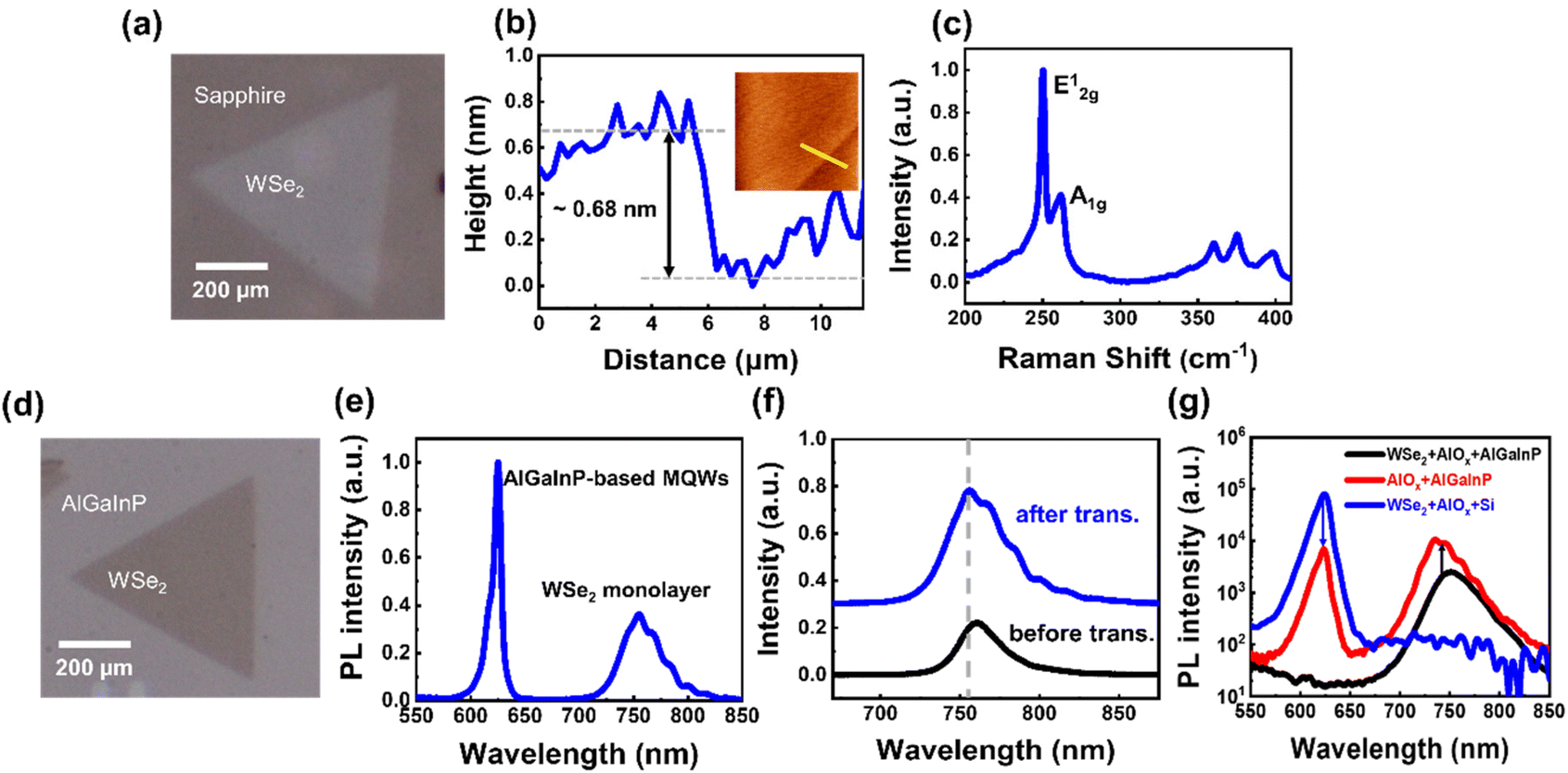 | ||
| Fig. 1 (a) Optical microscopy image of an as-grown WSe2 flake on sapphire. (b) AFM height profile of WSe2–AlGaInP (inset: AFM image of the sample). (c) Raman spectrum of the as-grown WSe2 flake on sapphire. (d) Optical microscopy image of the transferred WSe2 flake. (e) PL spectrum of monolayered WSe2–AlGaInP-based multiple quantum wells (MQWs). (f) PL spectra of the as-grown WSe2 and transferred WSe2. (g) PL spectra of the AlGaInP QWs (the blue line), WSe2 (the black line), and hybrid AlGaInP QW/WSe2 monolayer (the red line). | ||
To verify the optical properties of WSe2 on sapphire, a Raman spectrum was obtained with a 488 nm continuous-wave laser (Fig. 1(c)). The Raman spectrum shows two distinct peaks at 250.3 and 260 cm−1, respectively, which are labelled E12g and A1g. The E12g peak was generated by the in-plane vibration of tungsten and sulfur atoms, whereas the A1g peak corresponded to the out-of-plane vibration of selenium atoms. The observed peaks in the Raman spectrum are consistent with previous reports. A B12g peak at approximately 310 cm−1, which represents an interlayer interaction between the different WSe2 atomic layers, was not observed. This is indicative of WSe2 monolayers grown on a sapphire substrate. The AFM images and Raman spectrum were used to determine the number of WSe2 layers. The WSe2 monolayer grown on sapphire was then transferred onto an AlGaInP quantum well LED epilayer covered by an AlOx layer of thickness 30 nm. The optical microscope image of the transferred CVD-grown WSe2 monolayer, with the transfer being achieved using the PMMA-assisted transfer method, is displayed in Fig. 1(d). Fig. 1(e) shows the PL spectrum of the hybrid WSe2 monolayer/GaP-based structure by using a 532 nm wavelength laser. Two strong emission peaks associated with the AlGaInP quantum wells and the WSe2 monolayer are observed. To verify the emission properties of the WSe2 monolayer before and after the transfer process, the PL spectra of the transferred and as-grown WSe2 monolayers are characterized, and shown in Fig. 1(f). Compared with the spectrum of the as-grown WSe2 monolayer sample, that of the transferred WSe2 monolayer shows a peak that is blue-shifted. This small blue shift is attributed to the release of strain during the transfer process, where strain was caused by the difference in the thermal expansion coefficients of the CVD-grown WSe2 monolayer and sapphire substrate. The small oscillations in the PL spectrum are due to Fabry–Perot oscillations from the bottom AlGaInP MQW structure.
To investigate the interactions between the WSe2 monolayer and the AlGaInP QWs, we transferred WSe2 monolayers to the AlGaInP QW substrate and the AlOx substrate and characterized the PL spectra of the two WSe2 devices and the AlGaInP QW device. Fig. 1(g) shows the PL spectra of the AlGaInP QW (the blue solid line), the WSe2 monolayer (the black solid line) on AlOx substrate, and the hybrid WSe2 monolayer/AlGaInP QW (the red line) devices. The color conversion phenomena associated with the AlGaInP QWs and the WSe2 monolayer were observed. If the QWs and WSe2 monolayer were integrated into a single device, the corresponding PL intensities were reduced in the AlGaInP QW emission region but enhanced in the WSe2 emission region compared with the individual gain spectra. This result can be attributed to the energy transfer from the high energy medium (i.e. the AlGaInP QWs in the study) to the low energy medium (the WSe2 monolayer in the study).57,58 The color conversion efficiency η can be calculated as follows:
 | (1) |
Electrical measurements were conducted at room temperature and under ambient conditions by using arbitrary function generators to generate AC pulse square waves for driving the devices. The devices were connected to two probe stations, which contained tungsten probe tips for electrical testing. The signal was observed using a microscope objective lens. The signal passed through the 20 μm-wide entrance slit of the spectrometer and was then focused on a 600 g mm−1 grating to separate the light signal into spatial spectra.
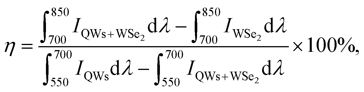
A 3D schematic and the vertical structure of the WSe2 monolayer–AlGaInP-based light-emitting device are shown in Fig. 2(a) and (b), respectively. The device consists of four components: two silver electrodes, emitter layers, and an insulating layer. The emitter layers comprise a WSe2 monolayer and the AlGaInP–GaInP multiple quantum well (MQW) active region. One of the electrodes serves as the bottom gate, while the other electrode serves as the source contact. Carriers are injected at the interface between the source contact and the semiconductor. To introduce an electric field into the insulating layer, a high-dielectric-constant AlOx film is selected as the insulating layer. The WSe2 monolayer is transferred onto the AlGaInP-based LED epilayer with an AlOx film inserted between the WSe2 monolayer and the LED epilayer to serve as a capacitive component. Electrodes are deposited on the top of the WSe2 layer and the surface of the bare LED epilayer to act as the source and gate electrodes, respectively. The left side of Fig. 2(c) shows the top-view scanning electron microscopy (SEM) image of the device at a magnification of 7000×. The geometry of the top electrode is a simple square window. The dark area enclosed by the dashed white line is the transferred WSe2 monolayer. Images of light emission from the device, captured using a charge-coupled device (CCD) camera, are shown on the right side of Fig. 2(c). The spatial distribution of the intensity of light emitted by the WSe2 monolayer and AlGaInP-based MQWs was nonuniform, which resulted from current crowding effects. In the WSe2 monolayer, this was because carrier injection and recombination occurred near the edge of the electrode. The thickness and composition of the layers in the device were determined through transmission electron microscopy (TEM) and energy-dispersive X-ray spectroscopy (EDX). Checking the thickness of WSe2 was extremely important because its properties strongly depend on the number of layers. Fig. 2(d) shows a bright-field scanning transmission electron microscopy (BF-STEM) image of the WSe2–AlOx–AlGaInP layered structure. Fig. 2(e) and (f) show the higher-magnification TEM images of the square area within the dotted blue line in Fig. 2(d) and of the GaInP–AlGaInP MQWs, respectively. The cross-sectional TEM image of WSe2 reveals that the thickness of single-layered WSe2 was approximately 0.7 nm, which perfectly matches the previous report of a monolayered WSe2 thickness. To further characterize the elemental composition of the layered structure, EDX was performed. The EDX elemental mapping images of WSe2–AlOx–AlGaInP shown in Fig. 2(g)–(j) indicate the spatial distribution of various elements over the structure. The distributions of W and Se were uniform. In addition, the presence of Al and Ga was expected due to the presence of the AlOx insulating layer and substrate of the AlGaInP-based LED.
 | ||
| Fig. 2 (a) Schematic of the hybrid WSe2 monolayer/AlGaInP-QW based light-emitting device. (b) Cross-sectional view of the device's structure. (c) SEM top view of the fabricated device (the dashed white line marks the region of transferred WSe2) and the intensity distributions of light emission from the device captured using a CCD camera. No color information is given in the images. (d) Cross-sectional BF-STEM image of the fabricated device. (e) Higher magnification of the square area within the dotted blue line in (d). (f) Cross-sectional TEM image of the AlGaInP–GaInP MQWs. The EDX mapping images and elemental analysis for (g)W, (h) Se, (i) Al and (j) Ga. | ||
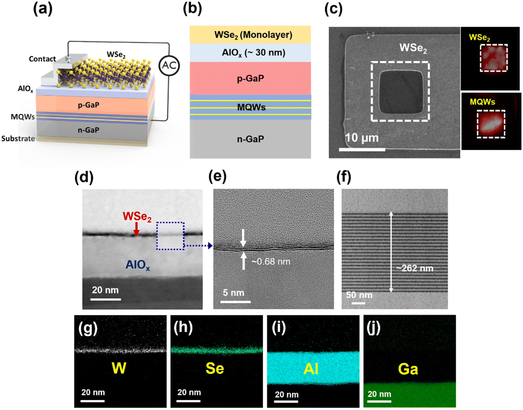
Fig. 3(a) shows the room-temperature EL spectra of the WSe2–AlGaInP-based light-emitting device driven by various voltages at a fixed frequency. For both the AlGaInP-based LED and WSe2, the EL intensity increased with the voltage. The inset of Fig. 3(a) shows the EL spectra for WSe2 emission at 1 MHz with increasing voltage. The spectra contain two distinguishable emission peaks at approximately 627 and 755 nm, corresponding to the AlGaInP-based MQWs and WSe2 monolayer, respectively. Because of the poor emission efficiency of the WSe2 monolayer, the EL peak intensity of WSe2 has been multiplied by a factor of 10 to better enable visualization. The peak at a wavelength of 627 nm in the red emission band with a full width at half maximum linewidth of 10 nm was attributed to the AlGaInP–InGaP MQWs, whereas the peak at a longer wavelength was attributed to the direct intralayer exciton emission of monolayered WSe2, in good agreement with previous works.59,60 The small oscillation due to Fabry–Perot interferences in the QW layer was also observed in the EL spectrum.
 | ||
| Fig. 3 (a) EL spectra of the device at various voltages at a fixed frequency (WSe2 emission at 1 MHz). (b) Voltage-dependent EL intensity of WSe2. (c) Semi-log plot of the voltage-dependent EL intensity of WSe2. EL intensity–voltage characteristic curves showing (d) Schottky emission and (e) FN emission at the metal–WSe2 interface. (f) Schematic band diagram of the metal–WSe2 interface upon a change in polarity of the AC voltage. | ||
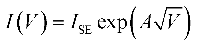
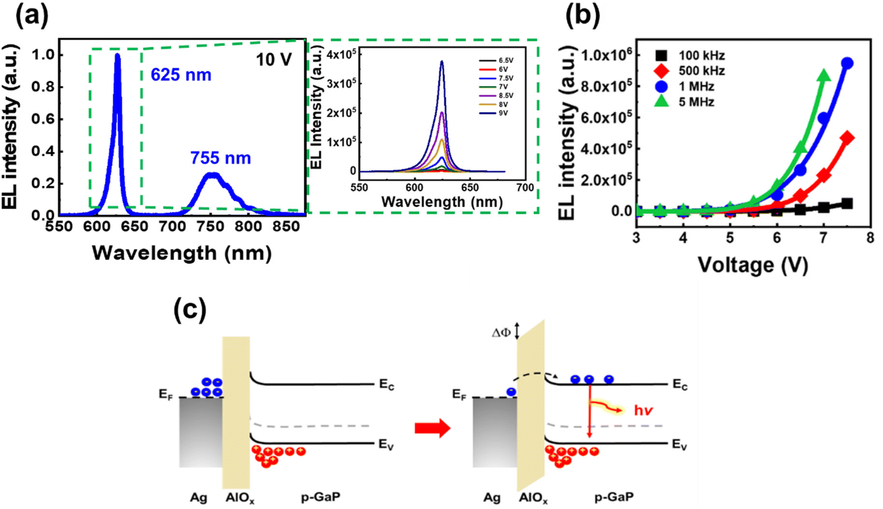
Fig. 3(b) shows the voltage-dependent peak EL intensity of WSe2 at constant frequencies. The EL intensity increases clearly as the operating voltage becomes larger than the threshold voltage. The threshold voltage (Vth) of the WSe2 monolayer, defined as the x-intercept of the linear portion of the EL intensity–voltage curve, was approximately 10 V (green line in Fig. 3(b)). As the operating frequency increases, the threshold voltage of the WSe2 monolayer emission decreases. No light emission was observed at voltages below Vth due to insufficient carrier injection from the Ag electrode. The EL intensity of WSe2 was proportional to the voltage above Vth. Recent studies have proposed the following empirical model of the relationship between the EL intensity and the voltage: IEL ∝ exp(ακV),61 where κ is the constant of the injected carrier concentration in the 2D semiconductor and α is the constant related to the characteristics of excitons. A semi-log plot of the EL intensity as a function of voltage is displayed in Fig. 3(c). This figure indicates a linear relationship between the logarithm of the EL intensity and the voltage, which conforms to the aforementioned model.
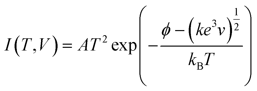
Research has revealed that thermionic emission and Fowler–Nordheim (FN) emission are the main mechanisms underlying charge transport through the Schottky contact at a metal–2D-material interface.62,63 The carrier injection efficiency is severely limited by the Schottky barrier at the metal–TMDC interface. To examine the mechanism of charge injection through the interface between the electrode and WSe2 under external electric field and room temperature conditions, we plotted ln(IEL) versus V1/2 and ln(IEL/V2) versus V−1. These curves represent thermionic-emission-like and FN-like behaviors, respectively. Thermionic emission is usually considered to occur at high temperatures; charges can acquire sufficient energy to overcome the Schottky barrier. When thermionic emission occurs without the presence of an external electric field, the current density can be described as a function of temperature, as in the Richardson–Dushman equation.64 However, if the effect of an electric field is considered, the current density can be expressed by a Schottky equation:65
 | (2) |
 .
.
According to the Schottky equation, the logarithmic EL intensity is proportional to the square root of the voltage. The thermionic emission plot, displayed in Fig. 3d, shows that the relationship between ln(IEL) and V1/2 is positive and linear in the low-voltage range (V < Vth; left-hand side of the red dotted line). Therefore, thermionic emission was considered to be the mechanism underlying carrier injection across the potential barrier at the Ag–WSe2 interface at a low voltage.
When a strong field is considered, carriers can tunnel through the barrier by a quantum mechanical effect. In quantum mechanical theory, the possibility of an electron penetrating a potential barrier is described by:66,67
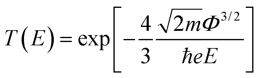 | (3) |
The tunneling probability depends on the width of the barrier. According to the barrier width equation x = Φ/eE, the width of barrier x is narrow when a strong electric field is applied. The tunneling of carriers occurs when the magnitude of the electric field is sufficiently high to change the barrier from being a flat band to having a triangular shape with a narrow effective width. This type of tunneling mechanism is known as FN tunneling.
The FN tunneling current equation is:
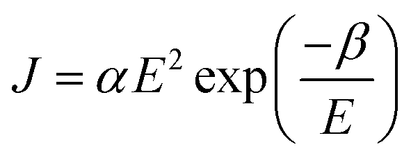 | (4) |
The AC-voltage-driven electroluminescence mechanism of 2D materials has been investigated previously.20,27,40Fig. 3(f) shows a schematic explaining the mechanism of electroluminescence of WSe2. In brief, by applying a steady negative bias to the back-gate electrode, holes accumulate at WSe2 and the Schottky barrier blocks the flow of holes from WSe2 to the metal electrode (Fig. 3(f), part marked 1). When the AC square-wave pulse signal changes from a negative to a positive polarity, the capacitive elements (i.e., AlOx) induce a potential difference between the top source and the back gate. The potential drop across the WSe2 layer causes conduction band bending and then leads to the tunneling of electrons from the electrode to WSe2. Subsequently, the holes generated in the previous step recombine with the injected electrons, which causes the release of a photon (Fig. 3(f), part marked 2). The same behavior is observed when the voltage switches from a positive to a negative polarity (Fig. 3(f), parts marked 3 and 4).
The peak values in the spectra presented in Fig. 3(a) were recorded, and the relationship between the EL intensity of the AlGaInP-based MQWs and the peak-to-peak voltage was discovered (Fig. 4(a) and (b)). By extrapolating the EL intensity–voltage curves, a threshold voltage of approximately 5.5 V was obtained. The EL intensity of the AlGaInP-based MQWs follows an empirical equation:
L = L0![[thin space (1/6-em)]](https://www.rsc.org/images/entities/char_2009.gif) exp(−β/V1/2) exp(−β/V1/2) | (5) |
 | ||
| Fig. 4 (a) EL spectra of the device at various voltages at a fixed frequency (AlGaInP-based MQW emission at 1 MHz). (b) Voltage-dependent EL intensity of AlGaInP-based MQWs. (c) Energy band diagram of the MIS structure of Ag–AlOx–p-GaP under zero bias and high bias conditions. | ||
The empirical equation fitted the experimental data favorably and indicated that the EL intensity increased superlinearly with an increase in the voltage.71,72 The EL peak intensity of both the AlGaInP-based LED and WSe2 was strongly dependent on voltage rather than current due to the capacitance characteristics of the device.73
Ag–AlOx–AlGaInP has a metal–insulator–semiconductor (MIS) structure. It comprises an insulating layer (AlOx) that separates the metal electrode and semiconductor. The process of radiative recombination in an AlGaInP-based LED53,74 is given as follows. When a positive AC bias voltage is applied to the gate electrode, the majority of carriers (holes) from the p-type region of the AlGaInP LED accumulate at the AlOx–p-GaP interface. The accumulated carriers cannot be injected into the Ag metal from the semiconductor because of the tunnel barrier, which is an insulating layer of AlOx with a thickness of a few tens of nanometers. The electrons can tunnel from the electrode to the semiconductor when a high positive voltage is applied because this reduces the effective barrier width (FN tunneling). Finally, the electrons recombine with holes and release energy in the form of a photon (as illustrated in Fig. 4(c)).
By estimating the internal quantum efficiency and the extraction efficiency of the devices, the external quantum efficiency (EQE) of the WSe2 monolayer and AlGaInP QWs devices are approximately 0.018% and 0.056%, as given in Fig. S2 and S3 of the ESI.† The device is operated under ambient conditions and no significant drop in efficiency was observed. It is worth noting that because the external quantum efficiency of the AlGaInP QW LED is larger than that of a WSe2 monolayer, the thickness of the AlOx layer, deposited through atomic layer deposition, can be controlled to manipulate the ratio of the EL intensity of the AlGaInP QWs to that of the WSe2 monolayer by controlling the light extraction efficiency and the threshold voltage. This is an important step to counterbalance the EL intensities of the AlGaInP QWs and the WSe2 monolayer. However, two-color emission was still achieved at a voltage greater than 10 V in the study. The AC driving conditions, and the device structure, can be further optimized in the future for better multi-color emission from the hybrid LED device.
Conclusions
In summary, we developed a multicolor AC-driven light-emitting device by integrating a WSe2 monolayer and AlGaInP–GaInP multiple quantum well (MQW) structures. The CVD-grown WSe2 monolayer was placed on the top of an AlGaInP-based light-emitting diode (LED) wafer to create a two-dimensional/three-dimensional heterostructure. The insulating layer, comprising AlOx, which was deposited through atomic layer deposition, is placed between these two materials and serves as a capacitor. The interfaces of the hybrid devices are characterized and verified with TEM images and EDX techniques. The device's room-temperature electroluminescence spectrum was found to contain two peaks that correspond to the emissions by the WSe2 monolayer and AlGaInP–InGaP MQWs, respectively. The voltage dependence of the electroluminescence intensity was characterized. The electroluminescence intensity–voltage characteristic curves indicated that thermionic emission was the mechanism underlying carrier injection across the potential barrier at the Ag–WSe2 monolayer interface at a low voltage, whereas Fowler–Nordheim emission was the mechanism at voltages higher than approximately 8.0 V. These multi-color hybrid light-emitting devices both expand the wavelength range of 2-D TMDC-based light emitters and support their implementation in applications such as chip-scale optoelectronic integrated systems, broad-band LEDs, and quantum display systems.Conflicts of interest
The authors declare no competing financial interest.Acknowledgements
This work was supported by research funding from Academia Sinica in Taiwan and the Ministry of Science and Technology (MOST) in Taiwan under Contract numbers MOST 110-2112-M-001-053 and MOST 111-2112-M-001-078.References
- A. Kuc, N. Zibouche and T. Heine, Influence of quantum confinement on the electronic structure of the transition metal sulfideTS2, Phys. Rev. B: Condens. Matter Mater. Phys., 2011, 83, 245213 CrossRef.
- K. F. Mak, C. Lee, J. Hone, J. Shan and T. F. Heinz, Atomically thin MoS(2): a new direct-gap semiconductor, Phys. Rev. Lett., 2010, 105(13), 136805 CrossRef PubMed.
- A. Splendiani, L. Sun, Y. Zhang, T. Li, J. Kim, C. Y. Chim, G. Galli and F. Wang, Emerging photoluminescence in monolayer MoS2, Nano Lett., 2010, 10(4), 1271–1275 CrossRef CAS PubMed.
- P. Tonndorf, R. Schmidt, P. Bottger, X. Zhang, J. Borner, A. Liebig, M. Albrecht, C. Kloc, O. Gordan, D. R. Zahn, S. Michaelis de Vasconcellos and R. Bratschitsch, Photoluminescence emission and Raman response of monolayer MoS(2), MoSe(2), and WSe(2), Opt. Express, 2013, 21(4), 4908–4916 CrossRef CAS PubMed.
- D. Andrzejewski, R. Oliver, Y. Beckmann, A. Grundmann, M. Heuken, H. Kalisch, A. Vescan, T. Kümmell and G. Bacher, Flexible Large–Area Light–Emitting Devices Based on WS2Monolayers, Adv. Opt. Mater., 2020, 8, 2000694 CrossRef CAS.
- F. Withers, O. Del Pozo-Zamudio, A. Mishchenko, A. P. Rooney, A. Gholinia, K. Watanabe, T. Taniguchi, S. J. Haigh, A. K. Geim, A. I. Tartakovskii and K. S. Novoselov, Light-emitting diodes by band-structure engineering in van der Waals heterostructures, Nat. Mater., 2015, 14(3), 301–306 CrossRef CAS PubMed.
- S. H. Bae, H. Kum, W. Kong, Y. Kim, C. Choi, B. Lee, P. Lin, Y. Park and J. Kim, Integration of bulk materials with two-dimensional materials for physical coupling and applications, Nat. Mater., 2019, 18(6), 550–560 CrossRef CAS PubMed.
- Y. Liu, N. O. Weiss, X. Duan, H.-C. Cheng, Y. Huang and X. Duan, van der Waals heterostructures and devices, Nat. Rev. Mater., 2016, 1, 16042 CrossRef CAS.
- W. Zhang, Q. Wang, Y. Chen, Z. Wang and A. T. S. Wee, van der Waals stacked 2D layered materials for optoelectronics, 2D Mater., 2016, 3, 022001 CrossRef.
- R. Cheng, S. Jiang, Y. Chen, Y. Liu, N. Weiss, H.-C. Cheng, H. Wu, Y. Huang and X. Duan, Few-layer molybdenum disulfide transistors and circuits for high-speed flexible electronics, Nat. Commun., 2014, 5(1), 5143 CrossRef CAS PubMed.
- X. Geng, Y. Yu, X. Zhou, C. Wang, K. Xu, Y. Zhang, C. Wu, L. Wang, Y. Jiang and Q. Yang, Design and construction of ultra-thin MoSe2 nanosheet-based heterojunction for high-speed and low-noise photodetection, Nano Res., 2016, 9(9), 2641–2651 CrossRef CAS.
- D. Kwak, M. Paur, K. Watanabe, T. Taniguchi and T. Mueller, High-Speed Electroluminescence Modulation in Monolayer WS2, Adv. Mater. Technol., 2022, 7(5), 2100915 CrossRef CAS.
- C. T. Phare, Y.-H. Daniel Lee, J. Cardenas and M. Lipson, Graphene electro-optic modulator with 30 GHz bandwidth, Nat. Photonics, 2015, 9(8), 511–514 CrossRef CAS.
- F. Sun, C. Nie, X. Wei, H. Mao, Y. Zhang and G. P. Wang, All-optical modulation based on MoS2-Plasmonic nanoslit hybrid structures, Nanophotonics, 2021, 10(16), 3957–3965 CrossRef CAS.
- Z. Sun, A. Martinez and F. Wang, Optical modulators with 2D layered materials, Nat. Photonics, 2016, 10(4), 227–238 CrossRef CAS.
- Y. Wang, F. Zhang, X. Tang, X. Chen, Y. Chen, W. Huang, Z. Liang, L. Wu, Y. Ge, Y. Song, J. Liu, D. Zhang, J. Li and H. Zhang, All-Optical Phosphorene Phase Modulator with Enhanced Stability Under Ambient Conditions, Laser Photonics Rev., 2018, 12(6), 1800016 CrossRef.
- O. Lopez-Sanchez, E. Alarcon Lladó, V. B. Koman, A. Fontcuberta i Morral, A. Radenovj and A. J. A. N. Kis, Light Generation and Harvesting in a van der Waals Heterostructure, ACS Nano, 2014, 8, 3042–3048 CrossRef CAS PubMed.
- J. Gu, B. Chakraborty, M. Khatoniar and V. M. Menon, A room-temperature polariton light-emitting diode based on monolayer WS2, Nat. Nanotechnol., 2019, 14(11), 1024–1028 CrossRef CAS PubMed.
- Y. Li, H. Sun, L. Gan, J. Zhang, J. Feng, D. Zhang and C.-Z. Ning, Optical Properties and Light-Emission Device Applications of 2-D Layered Semiconductors, Proc. IEEE, 2020, 108(5), 676–703 Search PubMed.
- D. H. Lien, M. Amani, S. B. Desai, G. H. Ahn, K. Han, J. H. He, J. W. Ager 3rd, M. C. Wu and A. Javey, Large-area and bright pulsed electroluminescence in monolayer semiconductors, Nat. Commun., 2018, 9(1), 1229 CrossRef PubMed.
- Y. Zhu, X. Sun, Y. Tang, L. Fu and Y. Lu, Two-dimensional materials for light emitting applications: Achievement, challenge and future perspectives, Nano Res., 2020, 14(6), 1912–1936 CrossRef.
- C. Wang, F. Yang and Y. Gao, The highly-efficient light-emitting diodes based on transition metal dichalcogenides: from architecture to performance, Nanoscale Adv., 2020, 2(10), 4323–4340 RSC.
- J. S. Ross, P. Klement, A. M. Jones, N. J. Ghimire, J. Yan, D. G. Mandrus, T. Taniguchi, K. Watanabe, K. Kitamura, W. Yao, D. H. Cobden and X. Xu, Electrically tunable excitonic light-emitting diodes based on monolayer WSe2 p-n junctions, Nat. Nanotechnol., 2014, 9(4), 268–272 CrossRef CAS PubMed.
- J. S. Ross, P. Rivera, J. Schaibley, E. Lee-Wong, H. Yu, T. Taniguchi, K. Watanabe, J. Yan, D. Mandrus, D. Cobden, W. Yao and X. Xu, Interlayer Exciton Optoelectronics in a 2D Heterostructure p-n Junction, Nano Lett., 2017, 17(2), 638–643 CrossRef CAS PubMed.
- D. Andrzejewski, E. Hopmann, M. John, T. Kummell and G. Bacher, WS2 monolayer-based light-emitting devices in a vertical p-n architecture, Nanoscale, 2019, 11(17), 8372–8379 RSC.
- D. Andrzejewski, H. Myja, M. Heuken, A. Grundmann, H. Kalisch, A. Vescan, T. Kümmell and G. Bacher, Scalable Large-Area p–i–n Light-Emitting Diodes Based on WS2 Monolayers Grown via MOCVD, ACS Photonics, 2019, 6(8), 1832–1839 CrossRef CAS.
- K. Han, G. H. Ahn, J. Cho, D.-H. Lien, M. Amani, S. B. Desai, G. Zhang, H. Kim, N. Gupta, A. Javey and M. C. Wu, Bright electroluminescence in ambient conditions from WSe2 p-n diodes using pulsed injection, Appl. Phys. Lett., 2019, 115, 011103 CrossRef.
- J. Wang, A. Rousseau, M. Yang, T. Low, S. Francoeur and S. Kena-Cohen, Mid-infrared Polarized Emission from Black Phosphorus Light-Emitting Diodes, Nano Lett., 2020, 20(5), 3651–3655 CrossRef CAS PubMed.
- H. Ou, H. Matsuoka, J. Tempia, T. Yamada, T. Takahashi, K. Oi, Y. Takaguchi, T. Endo, Y. Miyata, C. H. Chen, L. J. Li, J. Pu and T. Takenobu, Spatial Control of Dynamic p-i-n Junctions in Transition Metal Dichalcogenide Light-Emitting Devices, ACS Nano, 2021, 15, 12911–12921 CrossRef CAS PubMed.
- A. J. Watson, W. Lu, M. H. D. Guimarães and M. Stöhr, Transfer of large-scale two-dimensional semiconductors: challenges and developments, 2D Mater., 2021, 8, 032001 CrossRef CAS.
- G. Arutchelvan, C. J. Lockhart de la Rosa, P. Matagne, S. Sutar, I. Radu, C. Huyghebaert, S. De Gendt and M. Heyns, From the metal to the channel: a study of carrier injection through the metal/2D MoS2 interface, Nanoscale, 2017, 9(30), 10869–10879 RSC.
- D. Somvanshi, S. Kallatt, C. Venkatesh, S. Nair, G. Gupta, J. K. Anthony, D. Karmakar and K. Majumdar, Nature of carrier injection in metal/2D-semiconductor interface and its implications for the limits of contact resistance, Phys. Rev. B, 2017, 96, 205423 CrossRef.
- H. Choi, B. H. Moon, J. H. Kim, S. J. Yun, G. H. Han, S. G. Lee, H. Z. Gul and Y. H. Lee, Edge Contact for Carrier Injection and Transport in MoS2 Field-Effect Transistors, ACS Nano, 2019, 13(11), 13169–13175 CrossRef CAS PubMed.
- A. Jain, A. Szabo, M. Parzefall, E. Bonvin, T. Taniguchi, K. Watanabe, P. Bharadwaj, M. Luisier and L. Novotny, One-Dimensional Edge Contacts to a Monolayer Semiconductor, Nano Lett., 2019, 19(10), 6914–6923 CrossRef CAS PubMed.
- N. Wang, Ohmic contacts for atomically-thin transition metal dichalcogenide semiconductors, J. Semicond., 2020, 41, 070401 CrossRef CAS.
- P. C. Shen, C. Su, Y. Lin, A. S. Chou, C. C. Cheng, J. H. Park, M. H. Chiu, A. Y. Lu, H. L. Tang, M. M. Tavakoli, G. Pitner, X. Ji, Z. Cai, N. Mao, J. Wang, V. Tung, J. Li, J. Bokor, A. Zettl, C. I. Wu, T. Palacios, L. J. Li and J. Kong, Ultralow contact resistance between semimetal and monolayer semiconductors, Nature, 2021, 593(7858), 211–217 CrossRef CAS PubMed.
- Y. Zheng, J. Gao, C. Han and W. Chen, Ohmic Contact Engineering for Two-Dimensional Materials, Cell Rep. Phys. Sci., 2021, 2, 100298 CrossRef CAS.
- J. Cho, M. Amani, D. H. Lien, H. Kim, M. Yeh, V. Wang, C. Tan and A. Javey, Centimeter–Scale and Visible Wavelength Monolayer Light–Emitting Devices, Adv. Funct. Mater., 2019, 30, 1907941 CrossRef.
- Y. Zhu, B. Wang, Z. Li, J. Zhang, Y. Tang, J. F. Torres, W. Lipinski, L. Fu and Y. Lu, A High-Efficiency Wavelength-Tunable Monolayer LED with Hybrid Continuous-Pulsed Injection, Adv. Mater., 2021, 33(29), e2101375 CrossRef PubMed.
- V. Wang, Y. Zhao and A. Javey, Performance Limits of an Alternating Current Electroluminescent Device, Adv. Mater., 2021, 33(2), e2005635 CrossRef PubMed.
- G. Destriau, AC electroluminescence in ZnS, J. Chim. Phys., 1936, 33, 578 Search PubMed.
- M. Bredol and H. Schulze Dieckhoff, Materials for Powder-Based AC-Electroluminescence, Materials, 2010, 3(2), 1353–1374 CrossRef CAS.
- X. Cheng, Z. Zang, K. Yuan, T. Wang, K. Watanabe, T. Taniguchi, L. Dai and Y. Ye, A hybrid structure light-emitting device based on a CsPbBr3 nanoplate and two-dimensional materials, Appl. Phys. Lett., 2020, 116, 263103 CrossRef CAS.
- P. B. W. Jensen, J. Kjelstrup-Hansen and H.-G. Rubahn, Multicolor nanofiber based organic light-emitting transistors, Org. Electron., 2013, 14(12), 3324–3330 CrossRef CAS.
- X. Liu, J. Kjelstrup-Hansen, H. Boudinov and H.-G. Rubahn, Charge-carrier injection assisted by space-charge field in AC-driven organic light-emitting transistors, Org. Electron., 2011, 12(10), 1724–1730 CrossRef CAS.
- X. Liu, I. Wallmann, H. Boudinov, J. Kjelstrup-Hansen, M. Schiek, A. Lützen and H.-G. Rubahn, AC-biased organic light-emitting field-effect transistors from naphthyl end-capped oligothiophenes, Org. Electron., 2010, 11(6), 1096–1102 CrossRef CAS.
- H. Kajii, M. Yoshinaga, T. Karaki, M. Morifuji and M. Kondow, Microcavity polymer electroluminescent devices with solution-processed dielectric distributed Bragg reflectors utilizing inorganic copper(I) thiocyanate and insulating polymers, Org. Electron., 2021, 88, 106011 CrossRef CAS.
- M. Fröbel, T. Schwab, M. Kliem, S. Hofmann, K. Leo and M. C. Gather, Get it white: color-tunable AC/DC OLEDs, Light: Sci. Appl., 2015, 4(2), e247–e247 CrossRef.
- V. Wang and A. Javey, A Resonantly Driven, Electroluminescent Metal Oxide Semiconductor Capacitor with High Power Efficiency, ACS Nano, 2021, 15(9), 15210–15217 CrossRef CAS PubMed.
- Y. Zhao, V. Wang, D.-H. Lien and A. Javey, A generic electroluminescent device for emission from infrared to ultraviolet wavelengths, Nat. Electron., 2020, 3(10), 612–621 CrossRef CAS.
- S. M. Sadaf, Y. H. Ra, H. P. Nguyen, M. Djavid and Z. Mi, Alternating-Current InGaN/GaN Tunnel Junction Nanowire White-Light Emitting Diodes, Nano Lett., 2015, 15(10), 6696–6701 CrossRef CAS PubMed.
- S. Zhou, Y. Gao, C. Zheng, Y. Liu, H. Hu, J. Lv and X. Liu, A Comparative Study of GaN-Based Direct Current and Alternating Current High Voltage Light-Emitting Diodes, Phys. Status Solidi A, 2018, 215, 1700554 CrossRef.
- M. Hartensveld, B. Melanson, V. Thirupakuzi Vangipuram and J. Zhang, 450 nm Gallium Nitride Alternating Current Light-Emitting Diode, IEEE Photonics J., 2020, 12(6), 1–6 Search PubMed.
- K. Wang, Y. Liu, C. Wu, D. Li, S. Lv, Y. Zhang, X. Zhou and T. Guo, Electroluminescence from muLED without external charge injection, Sci. Rep., 2020, 10(1), 8059 CrossRef CAS PubMed.
- R. W. Hughes and M. Warner, LEDs driven by AC without transformers or rectifiers, Sci. Rep., 2021, 11(1), 963 CrossRef CAS PubMed.
- K. Wang, P. Chen, J. Chen, Y. Liu, C. Wu, J. Sun, X. Zhou, Y. Zhang and T. Guo, Alternating current electroluminescence from GaN-based nanorod light-emitting diodes, Opt. Laser Technol., 2021, 140, 107044 CrossRef CAS.
- C.-Y. Chang, C.-L. Yu, C.-A. Lin, H.-T. Lin, A. B. Lee, Z.-Z. Chen, L.-S. Lu, W.-H. Chang, H.-C. Kuo and M.-H. Shih, Hybrid Composites of Quantum Dots, Monolayer WSe2, and Ag Nanodisks for White Light-Emitting Diodes, ACS Appl. Nano Mater., 2020, 3(7), 6855–6862 CrossRef CAS.
- N. Taghipour, P. L. Hernandez Martinez, A. Ozden, M. Olutas, D. Dede, K. Gungor, O. Erdem, N. K. Perkgoz and H. V. Demir, Near-Unity Efficiency Energy Transfer from Colloidal Semiconductor Quantum Wells of CdSe/CdS Nanoplatelets to a Monolayer of MoS2, ACS Nano, 2018, 12(8), 8547–8554 CrossRef CAS PubMed.
- O. Karni, E. Barre, S. C. Lau, R. Gillen, E. Y. Ma, B. Kim, K. Watanabe, T. Taniguchi, J. Maultzsch, K. Barmak, R. H. Page and T. F. Heinz, Infrared Interlayer Exciton Emission in MoS2/WSe2 Heterostructures, Phys. Rev. Lett., 2019, 123(24), 247402 CrossRef CAS PubMed.
- S. Zhang, C. G. Wang, M. Y. Li, D. Huang, L. J. Li, W. Ji and S. Wu, Defect Structure of Localized Excitons in a WSe_{2} Monolayer, Phys. Rev. Lett., 2017, 119(4), 046101 CrossRef PubMed.
- M. Paur, A. J. Molina-Mendoza, R. Bratschitsch, K. Watanabe, T. Taniguchi and T. Mueller, Electroluminescence from multi-particle exciton complexes in transition metal dichalcogenide semiconductors, Nat. Commun., 2019, 10(1), 1709 CrossRef PubMed.
- F. Ahmed, M. S. Choi, X. Liu and W. J. Yoo, Carrier transport at the metal-MoS2 interface, Nanoscale, 2015, 7(20), 9222–9228 RSC.
- J. R. Duran Retamal, D. Periyanagounder, J. J. Ke, M. L. Tsai and J. H. He, Charge carrier injection and transport engineering in two-dimensional transition metal dichalcogenides, Chem. Sci., 2018, 9(40), 7727–7745 RSC.
- C. Herring and M. H. Nichols, Thermionic Emission., Rev. Mod. Phys., 1949, 21(2), 185–270 CrossRef CAS.
- W. Schottky, Emission of Electrons from an Incandescent Filament Under the Action of a Retarding Potential, Ann. Phys., 1914, 44, 1011–1032 CrossRef CAS.
- J. G. Simmons, Generalized Formula for the Electric Tunnel Effect between Similar Electrodes Separated by a Thin Insulating Film, J. Appl. Phys., 1963, 34(6), 1793–1803 CrossRef.
- E. L. Wolf, Principles of electron tunneling spectroscopy, Oxford University Press, Oxford, U.K, 1985 Search PubMed.
- J.-R. Chen, P. M. Odenthal, A. G. Swartz, G. C. Floyd, H. Wen, K. Y. Luo and R. K. Kawakami, Control of Schottky Barriers in Single Layer MoS2 Transistors with Ferromagnetic Contacts, Nano Lett., 2013, 13(7), 3106–3110 CrossRef CAS PubMed.
- D. H. Jung, S.-i. Kim and T. Kim, Characteristics of electrical metal contact to monolayer WSe2, Thin Solid Films, 2021, 719, 138508 CrossRef CAS.
- N. Kaushik, A. Nipane, F. Basheer, S. Dubey, S. Grover, M. M. Deshmukh and S. Lodha, Schottky barrier heights for Au and Pd contacts to MoS2, Appl. Phys. Lett., 2014, 105(11), 113505 CrossRef.
- D. Hu, X. Xu, J. Miao, O. Gidron and H. Meng, A Stretchable Alternating Current Electroluminescent Fiber, Materials, 2018, 11(2), 184 CrossRef PubMed.
- P. D. Rack and P. H. Holloway, The structure, device physics, and material properties of thin film electroluminescent displays, Mater. Sci. Eng., R, 1998, 21, 171–219 CrossRef.
- L. Wang, L. Xiao, H. Gu and H. Sun, Advances in Alternating Current Electroluminescent Devices, Adv. Opt. Mater., 2019, 7, 1801154 CrossRef.
- L.-C. Chen, C.-H. Hsu, X. Zhang and J.-R. Wu, Low-Cost ZnO:YAG-Based Metal-Insulator-Semiconductor White Light-Emitting Diodes with Various Insulators, Int. J. Photoenergy, 2014, 1–4 Search PubMed.
Footnote |
| † Electronic supplementary information (ESI) available. See DOI: https://doi.org/10.1039/d2nr03725d |
| This journal is © The Royal Society of Chemistry 2023 |