
In situ scanning tunneling microscopy studies of carbonate-induced restructuring of Ag-decorated Cu(100) electrodes†
Reihaneh
Amirbeigiarab
 and
Olaf M.
Magnussen
*
and
Olaf M.
Magnussen
*
Institute of Experimental and Applied Physics, Kiel University, Olshausenstr. 40, 24098 Kiel, Germany. E-mail: magnussen@physik.uni-kiel.de
First published on 8th September 2023
Abstract
Ag-decorated Cu electrocatalysts are of great interest for electrochemical CO2 reduction, because of an increased yield of multi-carbon products. Here, we present studies of well-defined AgCu electrodes by in situ scanning tunneling microscopy. These bimetallic model electrocatalysts are prepared by electrodepositing submonolayer Ag coverages on Cu(100) in 0.1 M H2SO4, resulting in monolayer islands with a hexagonal quasi-Ag(111) atomic lattice. Upon exchanging the solution at potentials in the double layer range to 0.1 M KHCO3, pronounced Ag island restructuring towards anisotropic shapes, the nucleation and growth of new islands, and a strong reduction in surface mobility are observed. In addition, high-resolution images reveal a highly disordered molecular adlayer, contrary to the case of Ag-free Cu(100) electrodes. These observations can be explained by interactions of metal adatoms with adsorbed (bi)carbonate and show that Ag redispersion on Cu electrocatalysts may occur even in the absence of CO2 reduction.
1 Introduction
In the context of sustainable energy conversion, the electrochemical reduction of carbon dioxide (CO2RR) to valuable chemicals and fuels is of great interest.1,2 Hence, design and development of highly efficient and selective catalysts for CO2RR is the focus of considerable current research. Numerous parameters affect the catalyst's properties and have to be considered in catalyst engineering, including the catalyst material, composition, morphology, defect density, and electrolyte composition.3,4 Among elemental metals, copper is unique in its ability to reduce CO2 to multi-carbon (C2+) products, such as ethylene or ethanol, with reasonable efficiency.2,5It has been shown that the Cu(100) surface is particularly favorable for the reduction of CO2 to C2+ products.2,6,7 However, pure copper as a catalyst cannot provide the required efficiency and C2+ selectivity. Several studies suggest that integration of a secondary metal species may be a promising approach to control and optimize the catalyst properties.8–11 Silver is a particularly interesting candidate, since it highly efficiently reduces CO2 to CO, which in combination with Cu, can enhance C2+ formation.11–15 Clark et al. reported a high selectivity toward the formation of multi-carbon products for CuAg bimetallic catalysts.12 Similar enhancements in the selectivity and activity were observed by Higgins et al. for CuAg thin films with nonequilibrium CuAg alloying.14 More recently, Herzog et al. showed that the Ag-decoration of Cu2O nanocubes can improve the faradaic efficiency of the liquid C2+ products, e.g. ethanol, 1-propanol and cetaldehyde.11 Here, full reduction of the Cu2O to Cu and strong redispersion of the Ag on the Cu surface was found after two hours of CO2RR. However, the metals remained phase-segregated in metallic Ag and Cu, which is in agreement with other studies15 as well as with the known immiscibility of Ag and Cu in the bulk.
Up to now, no detailed atomic-scale studies of CuAg bimetallic electrode surfaces under CO2RR conditions exist that could shed more light on the restructuring mechanisms. Previous in situ scanning tunneling microscopy (STM) studies have shown that Cu and Ag single crystal electrodes in sulfuric acid solution exhibit very high surface mobility.16–18 Thus, structural changes are in principle facile. First studies of a bimetallic CuAg system in the electrochemical environment were performed by Dietterle et al., who studied Cu electrodeposition on Ag(111) and Ag(100) electrodes in sulfuric acid solution.16,19 They observed the formation of isolated Cu islands without evidence for surface alloying. Nevertheless, even in the absence of surface alloy formation, substantial restructuring can occur in bimetallic systems due to differences in the surface energy of the two metals. For example, Ni submonolayer islands on Ag(111) electrodes were found to become partly embedded by Ag via step edge diffusion.20,21 Similar restructuring effects may be caused by adsorbate species such as anions that bind differently strong to the two metals. Especially for the case of Cu, adsorbate driven structural changes are well known (see ref. 22 for a recent overview).
In this work, we present in situ STM results on bimetallic CuAg model catalysts that reveal a strong influence of bicarbonate buffer solution, one of the most favored electrolytes for CO2RR, on the nanoscale morphology and molecular interface structure. For these studies, we employ Ag-decorated Cu(100) electrodes that are prepared in 0.1 M H2SO4via electrodeposition and initially characterized with atomic resolution in this solution. The restructuring process is initiated by exchange with 0.1 M KHCO3 and directly monitored by STM.
2 Experimental
All experiments were performed in electrochemical environment at room temperature, using a PicoPlus 5500 Scanning Probe Microscope (Agilent Inc., Santa Clara, USA). A Platinum wire was used as pseudo-reference electrode, calibrated via measurement vs. a standard calomel electrode (SCE). All potentials in this work are given vs. the reversible hydrogen electrode (RHE). Electrolytes were prepared from sulfuric acid (Merck, ultrapure), Ag sulfate (Alfa Aesar, 99.999%), potassium bicarbonate (Sigma-Aldrich, 99.7%), and ultrapure water. Prior to each experiment, the potassium bicarbonate electrolyte was purified from trace metal ion impurities using Chelex 100 Resin (Bio-Rad).23,24 Prior to each experiment, the Cu(100) electrode (MaTeck) was electropolished for at least three cycles (each cycle ca. 10 s) in 65–70% orthophosphoric acid (Merck) at potentials between 1.8 and 2.8 V vs. a Pt wire counter electrode. Immediately after each cycle, the single crystal was rinsed with ultrapure water (18.2 MΩ). For the STM measurements, tunneling currents of 0.05 to 1.5 nA and bias voltages of −0.27 to 0.04 V were used. The data analysis was performed via the SPIP (Scanning Probe Image Processor, Image Metrology A/S, Denmark) software. In some of the images, roughness filtering was applied to increase the contrast on the Cu terraces.The Ag-decorated Cu(100) were prepared in 0.1 M H2SO4 by introducing small amounts of silver-containing electrolyte (10–20 μM Ag2SO4) at a constant potential of ≈0.05 V into the electrochemical cell and waiting for ≈20 minutes. The coverages reported in this work were determined from the STM measurements and correspond to the fraction of the Cu surface covered by Ag islands in the STM images of a given sample. Different coverages between 0.1 and 0.7 monolayers (ML) were obtained by varying the Ag concentration in the solution. The necessary concentrations were estimated by employing the assumption that all Ag ions in the solution adsorb on the surface. The electrolyte exchange into the Ar-saturated 0.1 M KHCO3 was performed in the STM electrochemical cell under potential control, using syringe pumps (Hamilton) at a rate of 5 μL s−1. Considering that the electrolyte volume in the STM cell is ≈100 μL, we expect the actual exchange to occur in 20 s, albeit the exchange underneath the STM tip may be somewhat slower due to mass transport limitations.
3 Results and discussion
Ag-decorated Cu(100) in 0.1 M H2SO4
The in situ STM image in Fig. 1a shows the surface morphology of a freshly electropolished Cu(100) in 0.1 M H2SO4 at 0.05 V. Large, atomically smooth terraces can be seen, on which the (1 × 1) lattice of the Cu substrate is clearly visible (Fig. 1d). Adding Ag-containing solution (μM Ag2SO4) to the electrochemical cell results in the appearance of Ag islands. The size and number depend on the amount of silver contained in the solution, but the correlation between added Ag and island coverage estimated from the STM images is not strict. This is likely due to the very high mobility of silver atoms and islands on the Cu surface (see below) and the fact that the STM images observe only a local area, in which the coverage may differ from the average coverage on the entire surface. Two examples of Ag-decorated Cu(100) surfaces with Ag coverages of about 0.1 and 0.7 monolayers (ML) are presented in Fig. 1b and c, respectively. These STM images indicate that Ag islands are formed preferentially close to Cu step edges. The islands exhibit an apparent height of (0.08 ± 0.02) nm with respect to the neighboring Ag-free Cu substrate, which is clearly below the geometric height expected for Ag islands. This is commonly observed for bimetallic systems and can be attributed to electronic effects in the STM imaging.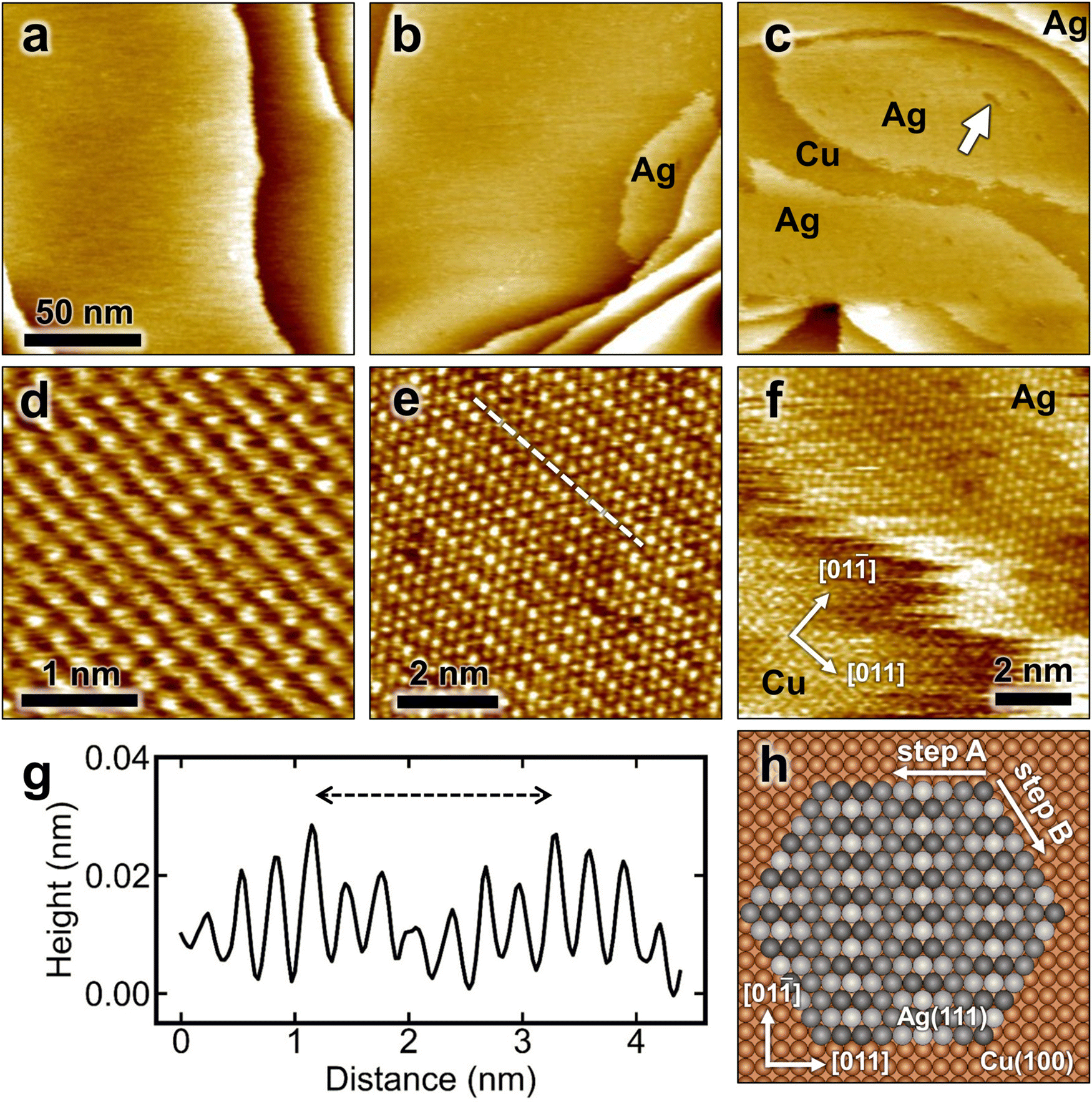 | ||
| Fig. 1 In situ STM images of Cu(100) surface (a) before and (b) and (c) after 0.1 ML and 0.7 ML Ag deposition at (b) 0.05 and (c) −0.04 V in 0.1 M H2SO4. (d)–(f) Atomic-resolution images of (d) the Cu(100) substrate lattice, (e) the atomic structure of the Ag islands, revealing a quasi-hexagonal structure with a long range modulation, and (f) the border between the Cu substrate and an Ag island (recorded at −0.04 V). The image in (f) shows that the Ag atomic rows along the direction of the long-range modulation are aligned with one of the close-packed directions of the underlying Cu lattice. (g) Apparent height profile along the white dashed line in (e), illustrating the long-range modulation of the Ag-decorated Cu(100). (h) Atomic model of Ag-adlayer, showing the corresponding modulation due to the different adsorption position of Ag on Cu(100). Different gray scales demonstrate the change of the apparent height in the STM images. | ||
High-resolution STM images of the Ag islands (Fig. 1e) reveal a pseudohexagonal lattice with a lattice parameter of ≈0.29 nm, which is close to the lattice distance in the Ag(111) plane. Furthermore, a characteristic uniaxial modulation along the Ag rows in [011] direction of the underlying Cu surface was observed, which can be attributed to the lattice mismatch with the underlying square lattice of the Cu(100) substrate (see Fig. 1e–g). This long-range modulation typically has a periodicity of 8 Cu lattice distances (i.e., ≈2 nm) or 7 interatomic distances of the Ag adlayer on top, respectively (Fig. 1e). This corresponds to an Ag–Ag spacing of 0.291 nm along this direction, which is very close to the nearest neighbor spacing in bulk Ag. Occasionally, also areas with larger periodicity of the modulation (≈8 Ag–Ag spacings over 9 Cu lattice distances) were found, indicating a slightly more compressed Ag lattice. The atomic modulation and the pseudohexagonal structure can be explained by an atomic arrangement within the Ag islands on Cu(100) as shown in Fig. 1h. It corresponds to an Ag in-plane structure that strongly resembles an Ag(111) surface that is aligned along one lattice direction with the Cu substrate. As illustrated in the model the Ag atoms are arranged along the [011] direction in between two atomic rows of Cu atoms, where they gradually change between fourfold-hollow and bridge sites. The different adsorption sites lead to a vertical modulation along the rows with the observed periodicity of 8 Cu lattice distances.
Both the steps of the Cu(100) substrate and the Ag island edges exhibit a characteristic frizziness (see Fig. 1f), which is a well-known phenomenon reported in previous STM studies of pure Cu and Ag surfaces.16–18,25 In these studies, the frizzy steps were shown to result from rapid kink motion along the steps, occurring on time scales that are fast compared to the time resolution of the STM. The high step-edge mobility was associated with the low cohesive energy of these metals. Consecutive STM images show also highly dynamic changes in the shape of the Ag islands, such as coalescence of Ag islands on time scales of minutes (see Fig. S1, grey arrows, ESI†). In addition, larger dark-appearing patches with lower mobility are visible within the islands, which are assigned to holes in the Ag layer based on the atomically resolved images (examples marked with white arrows in Fig. 1c and Fig. S1, ESI†). Also these fluctuate in between subsequent STM images. This highly dynamic character of Ag-decorated Cu(100) is in very good agreement with the calculated low diffusion barrier for silver on Cu(100).26,27
Our observations resemble results obtained for the growth of Ag on Cu(100) under ultrahigh vacuum (UHV) conditions.28 In this study, the formation of a surface alloy was proposed for Ag coverages up to 0.13 ML for temperatures close to room temperature and higher. At higher Ag concentrations, an alloying/dealloying process was suggested, where the dealloyed phase corresponded to a similar pseudohexagonal phase as observed in our work (apart from a slightly smaller Ag–Ag spacing of 0.285 nm along the Cu[011] direction) and likewise exhibited a significantly lower apparent height (≈0.03 nm) compared to monatomic Ag step edges. The latter was attributed to the formation of the quasi-Ag(111) islands within the Cu surface layer. In the present study, no evidence for surface alloying or embedding was observed, however. In particular, the fast dynamic fluctuations of the Ag island steps are hard to reconcile with embedding of the islands into the Cu surface layer, which should strongly block such step edge mobility. Furthermore, one would assume that the Cu would embed the Ag via step flow from adjacent terraces, as found in the case of embedded Ni islands on Ag(111),20,21 but no evidence for such step flow embedding is seen in the large scale STM images (Fig. 1b and c). We therefore regard it as highly likely that the islands correspond to a submonolayer of Ag on top of the Cu substrate.
Ag-decorated Cu(100) in 0.1 M KHCO3
The influence of bicarbonate buffer solution on the structure and morphology of CuAg bimetallic surfaces was addressed directly by in situ STM experiments. Here, the Ag-decorated Cu(100) surface was first prepared and characterized in the sulfuric acid solution, which was then exchanged with 0.1 M KHCO3 using a remote-controlled pump system. The latter allowed imaging the surface by STM during the change in electrolyte. However, the observed sample area changes considerably, because of substantial thermal drift during pump operation. Previous STM studies by our group showed that this exchange procedure results on clean Ag-free Cu(100) electrodes in a displacement of the sulfate by an ordered bicarbonate adlayer.29Fig. 2a shows the Ag-decorated copper surface at 0.05 V in sulfuric acid, before the electrolyte exchange has started. The surface exhibits flat terraces separated by atomic steps and covered by ≈0.1 ML of Ag islands. The subsequent STM images (Fig. 2b–f), recorded sequentially at time intervals of ≈105 s, show the evolution of the surface morphology shortly after the electrolyte exchange at 0.04 V. As discussed in the following, these images provide clear evidence of the substitution of adsorbed sulfate by a (bi)carbonate adlayer as well as structural modifications induced by the (bi)carbonate, including modifications of the Cu steps, changes of the Ag island shapes, and the appearance of new islands.
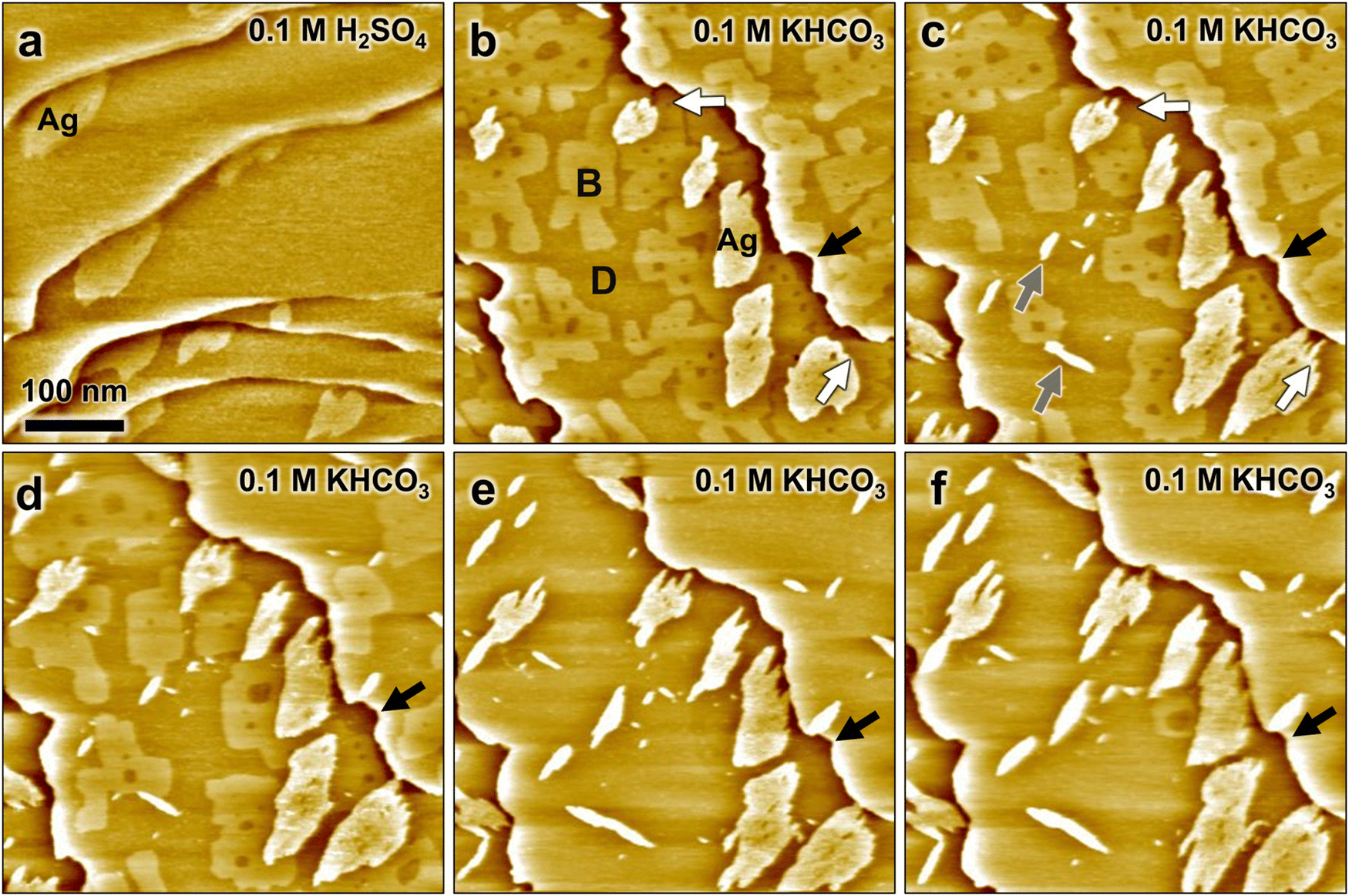 | ||
| Fig. 2 In situ STM images of Ag-decorated Cu(100), (a) in 0.1 M H2SO4 at 0.05 V, (b)–(f) recorded subsequently at 105 s intervals after exchange by 0.1 M KHCO3 at 0.04 V, with the image in (b) obtained 7 min after starting the electrolyte exchange. The images show the gradual replacement of adsorbed sulfate (areas B) by (bi)carbonate (areas D) as well as changes in the shape of Ag islands, nucleation of new islands, and modifications of the Cu steps. | ||
During the electrolyte exchange, three different type of areas with different appearance in the STM images are found on the Cu terraces: the Ag islands, bright appearing Cu surface areas, and dark appearing Cu areas (marked as Ag, B and D in Fig. 2b, respectively). The dark areas gradually expand on the surface with time, while the bright appearing areas shrink (Fig. 2b–d) and finally disappear (Fig. 2e and f). Based on the growth of the dark areas with increasing time after electrolyte exchange, we attribute those to Cu(100) covered by an adlayer of adsorbed (bi)carbonate. The bright areas are consequently assigned to remaining Cu(100) patches that are still covered by adsorbed sulfate. This assignment is supported by the roundish shape of the Ag steps that are directly adjacent to the bright areas, which resembles the Ag morphology found in sulfuric acid electrolyte. As both sulfate and carbonate chemisorb on Cu(100), the substitution apparently occurs only slowly via a nucleation and growth of (bi)carbonate adlayer islands.
Parallel to this change in adlayer structure, the Ag islands undergo significant restructuring. This restructuring occurs predominantly in the areas of type D that are assigned to the carbonate adlayer. Here, the islands develop a strongly anisotropic morphology with finger-like features (see e.g. areas marked with white arrows in Fig. 2b and c), which we attribute to the intrinsic anisotropy of the atomic-scale structure of the Ag monolayer. As discussed above, the mismatch between the hexagonal Ag lattice and the square Cu substrate results in a preferred direction within each island, in which close-packed atomic rows of Ag and Cu run parallel to each other (see Fig. 1f). Each island can adopt one out of two possible orientations, rotated by 90° with respect to each other. Consequently, the anisotropic morphology also can develop along two 90° rotated orientations, reflecting the atomic arrangement within the islands. Unfortunately, we did not succeed in resolving the metal lattice in bicarbonate electrolyte. However, based on the two-fold symmetry it appears likely that the preferred step direction of the anisotropic islands corresponds to that where the main lattice directions are parallel (steps A in Fig. 1h) rather than at 60° angles to each other (steps B in Fig. 1h).
A direct comparison of the island's shape and size in subsequent STM images reveals that the islands not only become anisotropic, but also change in size (see Fig. S2, ESI†). A rough estimate of the surface area of the Ag islands in Fig. 2b–f shows that within 210 s their size can increase from 10% to 50% in the bicarbonate electrolyte. Moreover, in areas B also new anisotropic islands arise (examples marked with gray arrows in Fig. 2c). These new islands are oriented along the same two directions as the anisotropic steps of the restructured Ag islands and also have a similar apparent height as the latter. We therefore assign also these new islands to Ag islands.
In addition to the changes in Ag island morphology, notable changes of the Cu steps are observed after the electrolyte exchange. In H2SO4 solution, the steps appear frizzy on the nanoscale but on larger scale are rather smooth. In contrast, directly after exchange by bicarbonate solution the steps exhibit indentations of several 10 nm in size with high local curvature. In the subsequent images these features in the steps gradually disappear again. An example of this step smoothening is marked by black arrows in Fig. 2b–f (see also Fig. S2, ESI†). In contrast to the findings in sulfuric acid, the steps no longer appear frizzy, suggesting a stabilization of the step edges due to (bi)carbonate adsorption. Similar observations have been reported in previous STM studies of Ag-free Cu(100) in bicarbonate solution29 and for Cu(100) covered by other chemisorbing adsorbates, e.g., Cl or Br.17,30
High-resolution STM images, recorded after full replacement of the sulfate by (bi)carbonate, show the molecular scale structure of the Ag-decorated Cu(100) at 0.04 V in bicarbonate electrolyte (Fig. 3). On the Cu terraces, a homogeneous disordered adlayer is unambiguously visible (see Fig. 3a and b). This adlayer differs strongly from that reported previously on bare Cu(100) in 0.1 M KHCO3, where highly ordered ( )R45° and (4 × 4) superstructures of coadsorbed (bi)carbonate and water were observed.29 Nevertheless, the average intermolecular distance within this disordered layer, determined via autocorrelation function analysis, is about 0.92 nm, which is quite close to the characteristic spacing between the most prominent maxima in both observed ordered adlayer structures, suggesting that the adlayer is composed predominantly of (bi)carbonate. The disordered arrangement has to be attributed to the presence of Ag on the surface. Possible scenarios how Ag affects the adlayer on Cu(100) will be discussed further below.
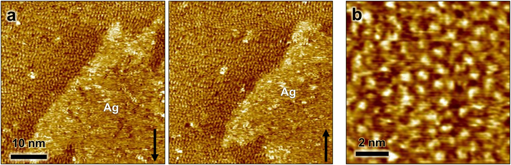 | ||
| Fig. 3 High-resolution in situ STM images of the Ag-decorated Cu(100) in 0.1 M KHCO3 at 0.04 V, showing (a) two successively recorded images of an Ag island and the neighboring Cu terrace and (b) a smaller scale image of the disordered adlayer on the Cu(100) surface. | ||
On top of the Ag islands, the high-resolution images show likewise a disordered arrangement that often appears fuzzy (Fig. 3a). As the molecular structure on the neighboring Cu terrace is clearly resolved in the images, this appearance indicates a high mobility of the adlayer on the Ag islands. Furthermore, local maxima and minima in this arrangement fluctuate strongly in successively recorded STM images, supporting a high adlayer mobility. These observations suggest a distinctly different adlayer structure on the Ag monolayer as compared to that on Cu(100). On Cu(100), both theoretical calculations and spectroscopic experiments suggest a bidentate adsorption on Cu(100), whereas a nearly planar adsorption of carbonate on Ag(111) surfaces has been proposed on the basis of theoretical calculations as well as spectroscopy experiments in the gas phase.31–33 Assuming that the Ag islands maintain the pseudo-Ag(111) structure in 0.1 M KHCO3, this difference in adsorption geometry can explain the different appearance in the STM images. A high surface mobility of planar carbonate on a hexagonally close-packed Ag surface seems plausible, but calculations that would confirm this do not exist yet.
To get insight to the origin of these changes in the molecular-scale adlayer structure and nanoscale surface morphology during and after the electrolyte replacement, it is beneficial to compare the dynamic behavior of the Ag-decorated Cu(100) surface in both electrolytes. Although a quantitative analysis of the dynamic is impossible due to the limited temporal resolution of the STM, there are clear indications of a decreased surface mobility of metal adatoms on the (bi)carbonate covered surface. In particular, the absence of frizzy steps at both Cu(100) terrace and Ag island edges (see Fig. 3a) supports this hypothesis. Because of this lower mobility, Cu and Ag adatoms are initially trapped on the Cu terraces after substitution of the adsorbed sulfate by (bi)carbonate. However, the adatoms still retain some mobility and, on longer time scales, can attach to existing steps or form nuclei of new islands (see Fig. 2 and Fig. S3, ESI†). The former leads to changes in the shape of the Ag islands and Cu steps, the latter to the formation and growth of additional islands. We note that also the anisotropy of the Ag islands in the presence of adsorbed (bi)carbonate may be a direct consequence of the lowered mobility. This is suggested by the STM studies of Ag-decorated Cu(100) under UHV conditions, where likewise anisotropically shaped islands were observed at lower temperatures, i.e., reduced surface mobility.28
The disordered adlayer structure can be explained as well by the presence of (slowly diffusing) Ag and Cu adatoms. Very similar disordered adlayer structures were recently observed by us in STM studies of Cu(100) in 0.1 M KHCO3 after Cu adatoms were formed on the surface due to surface restructuring at potentials below −0.2 V.34 The main difference in the present case is that adatoms of two metal species exist on the surface, which are embedded and diffusing within the molecular adlayer, preventing the formation of highly ordered (bi)carbonate layers. All these observations underline the crucial role of the adsorbed (bi)carbonate in the morphology of the electrocatalyst, even in a potential range well above that typically associated with the onset of the CO2 reduction.
Finally, we address the question whether the observed surface restructuring may be caused by the CO2RR itself. Although CO2RR is in principle thermodynamically possible in the potential range used in our studies,2 it is typically observed only at large overpotentials, for example, at potentials ≤−0.5 V for Ag-free and Ag-decorated Cu nanoparticles.11 However, locally, the initial steps of the reaction, such as the formation of reaction intermediates, may occur at considerably more positive potentials. In our recent study of clean Cu(100) electrodes in 0.1 M KHCO3, a restructuring of the surface via formation of Cu nanoclusters, which could be assigned to generation of CO, was observed already near −0.2 V.34 It cannot be unambiguously excluded that the restructuring of the Ag islands is caused by a similar effect, occurring at even more positive potentials. Nevertheless, we regard this idea as less likely, as CO and other relevant CO2RR intermediates adsorb less strongly on Ag than on Cu.35 This is also supported by a recent surface-enhanced Raman spectroscopy study of nanoporous CuAg electrodes in 0.1 M KHCO3, where CO and COOH adsorbates were only adsorbed at ≤−0.3 V, that is, at considerably more negative potentials.36
4 Conclusion
In this work, we introduced a procedure to prepare well-defined bimetallic CO2RR model catalysts, specifically Cu(100) electrodes decorated with Ag sub-monolayer islands, and to study them in bicarbonate electrolyte. Our in situ STM data indicate a quasi-Ag(111) hexagonal structure of these islands, comparable to the structure found under UHV conditions, and revealed pronounced restructuring of the Ag islands and Cu steps, the formation of new islands, changes in the molecular-scale adlayer structure, and a modified surface mobility. While strong restructuring was also found in previous studies of AgCu electrocatalysts in bicarbonate solution, the latter monitored the sample morphology only before and after the reaction and attributed the structural changes to reduction-driven process during the CO2RR and changes induced by Cu oxidation/reduction. Our results demonstrate that the mere presence of adsorbed (bi)carbonate has a pronounced influence on the surface morphology and dynamics of this bimetallic electrode, even at potentials where no major reactions occur. The resulting restructuring processes lead to a redistribution of Ag atoms already at potentials in the double layer regime, which needs to be considered for a true understanding of bimetallic CO2RR electrocatalysts, especially for studies under potentiodynamic conditions. Furthermore, considering that polycrystalline Cu was reported to undergo substantial restructuring to Cu(100),37,38 the observed restructuring of Ag surface atoms should also be relevant for realistic CuAg electrocatalysts.Author contributions
R. A. performed the STM measurements including the data analysis, O. M. M. conceived the studies and was responsible for project administration, O. M. M., R. A. contributed to writing the original manuscript.Conflicts of interest
The authors declare no conflict of interest.Acknowledgements
We gratefully acknowledge financial support by the Deutsche Forschungsgemeinschaft (DFG, German Research Foundation) via SPP 2080, project no. 406944504.References
- P. De Luna, C. Hahn, D. Higgins, S. A. Jaffer, T. F. Jaramillo and E. H. Sargent, Science, 2019, 364, eaav3506 CrossRef PubMed.
- S. Nitopi, E. Bertheussen, S. B. Scott, X. Liu, A. K. Engstfeld, S. Horch, B. Seger, I. E. Stephens, K. Chan, C. Hahn, J. K. Nørskov, T. F. Jaramillo and I. Chorkendorff, Chem. Rev., 2019, 119, 7610–7672 CrossRef CAS PubMed.
- Y. Y. Birdja, E. Pérez-Gallent, M. C. Figueiredo, A. J. Göttle, F. Calle-Vallejo and M. T. Koper, Nat. Energy, 2019, 4, 732–745 CrossRef CAS.
- H. Mistry, A. S. Varela, S. Kühl, P. Strasser and B. R. Cuenya, Nat. Rev. Mater., 2016, 1, 1–14 Search PubMed.
- Y. Hori, Electrochemical CO2 Reduction on Metal Electrodes, Springer, 2008, pp. 89–189 Search PubMed.
- K. Jiang, R. B. Sandberg, A. J. Akey, X. Liu, D. C. Bell, J. K. Nørskov, K. Chan and H. Wang, Nat. Catal., 2018, 1, 111–119 CrossRef CAS.
- G. Zhang, Z. J. Zhao, D. Cheng, H. Li, J. Yu, Q. Wang, H. Gao, J. Guo, H. Wang, G. A. Ozin, T. Wang and J. Gong, Nat. Commun., 2021, 12, 1–11 CrossRef PubMed.
- D. Kim, J. Resasco, Y. Yu, A. M. Asiri and P. Yang, Nat. Commun., 2014, 5, 1–8 Search PubMed.
- S. Ma, M. Sadakiyo, M. Heim, R. Luo, R. T. Haasch, J. I. Gold, M. Yamauchi and P. J. Kenis, J. Am. Chem. Soc., 2017, 139, 47–50 CrossRef CAS PubMed.
- M. Bernal, A. Bagger, F. Scholten, I. Sinev, A. Bergmann, M. Ahmadi, J. Rossmeisl and B. R. Cuenya, Nano Energy, 2018, 53, 27–36 CrossRef CAS.
- A. Herzog, A. Bergmann, H. S. Jeon, J. Timoshenko, S. Kühl, C. Rettenmaier, M. Lopez Luna, F. T. Haase and B. Roldan Cuenya, Angew. Chem., Int. Ed., 2021, 60, 7426–7435 CrossRef CAS PubMed.
- E. L. Clark, C. Hahn, T. F. Jaramillo and A. T. Bell, J. Am. Chem. Soc., 2017, 139, 15848–15857 CrossRef CAS PubMed.
- S. Lee, G. Park and J. Lee, ACS Catal., 2017, 7, 8594–8604 CrossRef CAS.
- D. Higgins, A. T. Landers, Y. Ji, S. Nitopi, C. G. Morales-Guio, L. Wang, K. Chan, C. Hahn and T. F. Jaramillo, ACS Energy Lett., 2018, 3, 2947–2955 CrossRef CAS.
- A. Dutta, I. Z. Montiel, R. Erni, K. Kiran, M. Rahaman, J. Drnec and P. Broekmann, Nano Energy, 2020, 68, 104331 CrossRef CAS.
- M. Dietterle, T. Will and D. M. Kolb, Surf. Sci., 1995, 342, 29–37 CrossRef CAS.
- M. R. Vogt, A. Lachenwitzer, O. M. Magnussen and R. J. Behm, Surf. Sci., 1998, 399, 49–69 CrossRef CAS.
- M. Giesen, R. Randler, S. Baier, H. Ibach and D. Kolb, Electrochim. Acta, 1999, 45, 527–536 CrossRef CAS.
- M. Dietterle, T. Will and D. M. Kolb, Surf. Sci., 1998, 396, 189–197 CrossRef CAS.
- S. Morin, A. Lachenwitzer, F. Möller, O. Magnussen and R. Behm, J. Electrochem. Soc., 1999, 146, 1013–1018 CrossRef CAS.
- F. Maroun, S. Morin, A. Lachenwitzer, O. Magnussen and R. Behm, Surf. Sci., 2000, 460, 249–263 CrossRef CAS.
- A. Auer and J. Kunze-Liebhäuser, Structure-activity relations of Cu-based single-crystal model electrocatalysts, Elsevier, 2023 Search PubMed.
- A. Wuttig and Y. Surendranath, ACS Catal., 2015, 5, 4479–4484 CrossRef CAS.
- D. Gao, I. T. McCrum, S. Deo, Y.-W. Choi, F. Scholten, W. Wan, J. G. Chen, M. J. Janik and B. Roldan Cuenya, ACS Catal., 2018, 8, 10012–10020 CrossRef CAS.
- M. Giesen, Prog. Surf. Sci., 2001, 68, 1–154 CrossRef CAS.
- D. E. Sanders and A. E. DePristo, Surf. Sci., 1992, 260, 116–128 CrossRef CAS.
- H. Yildirim and T. S. Rahman, Phys. Rev. B: Condens. Matter Mater. Phys., 2009, 80, 1–9 CrossRef.
- P. Sprunger, E. Lægsgaard and F. Besenbacher, Phys. Rev. B: Condens. Matter Mater. Phys., 1996, 54, 8163–8171 CrossRef CAS PubMed.
- R. Amirbeigiarab, A. Bagger, J. Tian, J. Rossmeisl and O. M. Magnussen, Angew. Chem., Int. Ed., 2022, 61, e202211360 CrossRef CAS PubMed.
- P. Broekmann, M. Anastasescu, A. Spaenig, W. Lisowski and K. Wandelt, J. Electroanal. Chem., 2001, 500, 241–254 CrossRef CAS.
- J. Knudsen, N. M. Martin, E. Grånäs, S. Blomberg, J. Gustafson, J. N. Andersen, E. Lundgren, S. Klacar, A. Hellman and H. Grönbeck, Phys. Rev. B: Condens. Matter Mater. Phys., 2011, 84, 1–6 CrossRef.
- K. Isegawa, K. Ueda, S. Hiwasa, K. Amemiya, K. Mase and H. Kondoh, Chem. Lett., 2019, 48, 159–162 CrossRef CAS.
- E. Patrito and P. P. Olivera, Electrochim. Acta, 1998, 44, 1237–1245 CrossRef CAS.
- R. Amirbeigiarab, J. Tian, A. Herzog, C. Qiu, A. Bergmann, B. Roldan Cuenya and O. M. Magnussen, Nat. Catal., 2023 DOI:10.1038/s41929-023-01009-z.
- C. Shi, H. A. Hansen, A. C. Lausche and J. K. Norskov, Phys. Chem. Chem. Phys., 2014, 16, 4720–4727 RSC.
- W. Shan, R. Liu, H. Zhao and J. Liu, J. Phys. Chem. Lett., 2022, 13, 7296–7305 CrossRef CAS PubMed.
- Y.-G. Kim, J. H. Baricuatro and M. P. Soriaga, Electrocatalysis, 2018, 9, 526–530 CrossRef CAS.
- S. H. Lee, J. C. Lin, M. Farmand, A. T. Landers, J. T. Feaster, J. E. Avilés Acosta, J. W. Beeman, Y. Ye, J. Yano, A. Mehta, R. C. Davis, T. F. Jaramillo, C. Hahn and W. S. Drisdell, J. Am. Chem. Soc., 2021, 143, 588–592 CrossRef CAS PubMed.
Footnote |
| † Electronic supplementary information (ESI) available. See DOI: https://doi.org/10.1039/d3cp02766j |
| This journal is © the Owner Societies 2023 |