DOI:
10.1039/D2NR04321A
(Paper)
Nanoscale, 2022,
14, 15663-15668
Nano-optical imaging of exciton–plasmon polaritons in WSe2/Au heterostructures†
Received
6th August 2022
, Accepted 8th October 2022
First published on 10th October 2022
Abstract
We report a nano-optical imaging study of exciton–plasmon polaritons (EPPs) in WSe2/Au heterostructures with scattering-type scanning near-field optical microscopy (s-SNOM). By mapping the interference fringes of EPPs at various excitation energies, we constructed the dispersion diagram of the EPPs, which shows strong exciton–plasmon coupling with a sizable Rabi splitting energy (∼0.19 eV). Furthermore, we found a sensitive dependence of the polariton wavelength (λp) on WSe2 thickness (d). When d is below 40 nm, λp decreases rapidly with increasing d. As d reaches 50 nm and above, λp drops to 210 nm, which is over 4 times smaller than that of the free-space photons. Our simulations indicate that the high spatial confinement of EPPs is due to the strong localization of the polariton field inside WSe2. Our work uncovers the transport properties of EPPs and paves the way for future applications of these highly confined polaritons in nanophotonics and optoelectronics.
Introduction
Exciton–plasmon polaritons (EPP) are hybrid nanophotonic modes formed due to the coupling of surface plasmons polaritons (SPPs) with excitons – bound states of electrons and holes.1–11 Due to the field localization and enhancement of SPPs, the hybrid EPPs often demonstrate strong plasmon–exciton interactions, which is ideal for many potential applications, including surface-enhanced Raman spectroscopy, solar harvesting, and polariton emission.11 Common EPP devices are constructed using noble metals interfacing a variety of excitonic materials, including organic molecules and semiconductors. While organic molecules support strongly bounded excitons, they often suffer from fast degradations at elevated temperatures or upon exposure to air and light. Therefore, crystalline semiconductors are often used to enable high device stability under long-term usage. Traditional III–V semiconductors (e.g., GaAs, GaN, etc.) with an exciton binding energy of 20–30 meV support exciton polaritons (EPs) and EPPs at cryogenic temperatures.1,12–15 In recent years, van der Waals (vdW) semiconductors have been widely explored in polaritonic studies due to their strongly-bound excitons.16–22 The exciton binding energy of these vdW materials is 60–100 meV in the bulk and can reach hundreds of meV when thinning to atomic layers.23–26 As a result, EPs and EPPs in these layered semiconductors are stable even at room temperature. So far, studies of EPPs in vdW semiconductors were mainly performed with far-field spectroscopy.5–10 Real-space imaging studies of these hybrid modes have not been reported.
In this work, we performed a comprehensive nano-optical imaging study of EPPs in heterostructures of thin tungsten diselenide (WSe2) flakes on gold (Au) films. WSe2 is a group IVB transition metal dichalcogenide (TMD) and a prototypical vdW semiconductor. The two neutral excitons (i.e., A- and B-excitons) of WSe2 are at around 1.6 eV and 2.1 eV, respectively.21,27 The WSe2 thin-flake samples used in our experiments were prepared by mechanical exfoliation of bulk WSe2 and were then transferred onto a thin Au film on a silicon wafer. For nano-optical imaging, we employed a scattering-type scanning near-field optical microscope (s-SNOM) that was built on an atomic force microscope (AFM). The s-SNOM probes used in our work were metal-coated silicon tips with a radius of curvature of ∼25 nm at their apex, which defines the spatial resolution. For EPP excitations (see Fig. 1a), we illuminated the s-SNOM probe with a continuous-wave Ti:sapphire laser. The spectral range of the laser is 1.3–1.8 eV, which covers the A-exciton energy of WSe2. The laser is set to be in p polarization, which is ideal for the tip enhancement and the excitation of SPPs and EPPs.
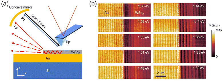 |
| | Fig. 1 (a) Illustration of nano-optical imaging experiment of a WSe2/Au heterostructure sample. (b) The near-field amplitude images of a typical WSe2/Au heterostructure taken at various excitation energies. The white dashed line marks the edge of the WSe2 flake. | |
Results and discussion
Near-field imaging of EPPs
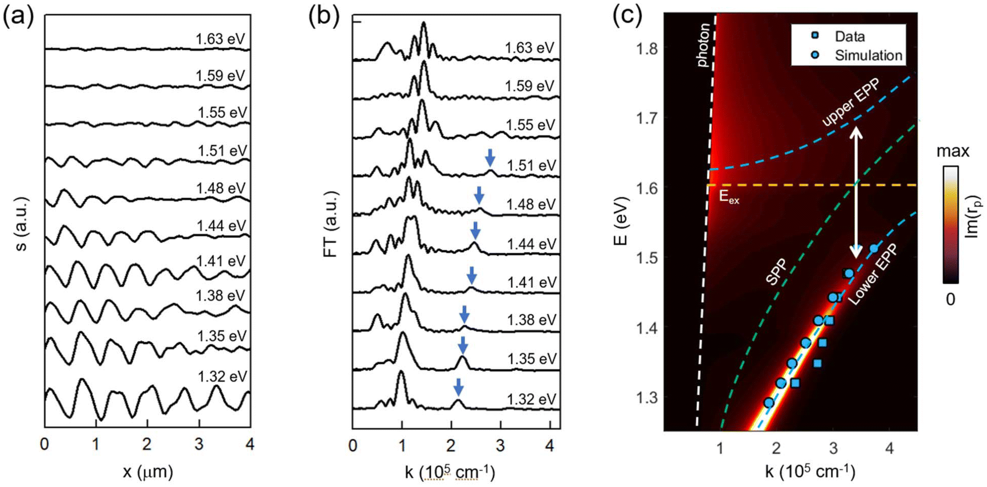
In Fig. 1b, we plot the near-field amplitude images obtained with s-SNOM at various excitation energies (E) on a typical WSe2/Au heterostructure sample. In this sample, the thickness of WSe2 (d) is 45 nm, and the thickness of the Au film is 100 nm. As illustrated in Fig. 1a, the WSe2 flake is on the right half of the images, and the bare Au film is on the left. We used white dashed lines to mark the edge of the WSe2 flake in Fig. 1b. The laser beam is aligned perpendicular to the WSe2 edge. From Fig. 1b, one can observe bright fringes on both the Au and WSe2 sides of the sample. These fringes are parallel to the WSe2 edge and extend microns away from the edge. By tuning the laser energy, we found that the fringe pattern demonstrates a systematic variation. As introduced in previous studies,20–22,28–30 such fringes are generated due to the interference between tip-backscattered photons [labeled as “P1” in Fig. 1a] and beam paths involving propagative in-plane modes. A common type of beam path is labeled as “P2” in Fig. 1a, where tip-excited in-plane modes propagate toward the edge of WSe2 and then get scattered into photons that are collected by the detector. In the ESI (Fig. S9†), we discuss another possible beam path that is responsible for the generation of the interference fringes. The in-plane modes responsible for the interference fringes on the Au side are SPPs (see Fig. S3 in ESI†). In the main text, we discuss mainly the fringes on the WSe2 side. Based on the interference mechanism involving beam paths ‘P1’ and ‘P2’ (Fig. 1a), we can establish a direct relationship between the fringe period (ρ) and the wavelength of the in-plane mode (λp):20–22| | 1/ρ = 1/λp − cos![[thin space (1/6-em)]](https://www.rsc.org/images/entities/char_2009.gif) α/λ0, α/λ0, | (1) |
where λ0 is the free-space photon wavelength and α is the incident angle of the laser beam (α ≈ 30°) [see Fig. 1a].
Dispersion analysis of EPPs
To obtain ρ and hence λp, we extracted the line profiles perpendicular to the fringes on WSe2 from Fig. 1b, which are plotted in Fig. 2a. We then performed a Fourier transform (FT) of these profiles to determine ρ. The corresponding FT profiles are plotted in Fig. 2b, where the peaks correspond to 2π/ρ. Here, we noticed two peaks in the FT profiles. The one at a relatively high wavenumber (k) corresponds to interference fringes of EPPs generated by beam paths ‘P1’ and ‘P2’. The lower-k peak, which sits roughly at half the k coordinates, is generated due to a more complicated interference process involving additional beam paths (see detailed discussions in the ESI†). With Fourier analysis and eqn (1), we were able to determine λp and mode wavevector (kp = 2π/λp) at various excitation energies, based on which we constructed the E − kp dispersion relationship of the in-plane mode. The experimental dispersion is shown in Fig. 2c as squares. Besides, we also plot the dispersion relation obtained from finite-element simulations (circles) (see Fig. S4 in ESI†). Both data points are sitting on a theoretical dispersion colormap, where we plot the imaginary part of the p-polarized reflection coefficient (rp). The bright curves revealed by the colormap correspond to the photonic or polaritonic modes in the system. Here we can see a high-wavevector mode on the right side of the photon line, which matches well the experimental and simulation data points.
 |
| | Fig. 2 (a) Energy-dependent fringe profiles (background subtracted) extracted from near-field images in Fig. 1. (b) Fourier-transform (FT) of the fringe profiles in panel (a). The arrows mark the peak associated with EPP interference involving beam paths ‘P1’ and ‘P2’. (c) Dispersion diagrams of EPPs in a 45-nm-thick WSe2 flake on a thin Au film obtained from theoretical calculations (colormap), experimental data (squares), and finite-element simulations (circles). The colormap plots the imaginary part of the reflection coefficient Im(rp). The white and orange dashed lines mark the free-space photon and A-exciton energy. The green dashed curves mark the SPP mode without coupling with excitons (see Fig. S5 in ESI†). The blue dashed curves mark the upper and lower branches of the EPP mode. | |
The bright mode marked with blue dashed curves in Fig. 2c corresponds to the EPP mode, which is generated due to the coupling between the SPP mode of Au and the A exciton of WSe2. Due to the coupling, the bare plasmonic mode is split into two polaritonic branches (upper and lower branches). The Rabi splitting energy ΩR of the two branches is estimated to be 0.19 eV (marked with arrow), higher than the average linewidth of exciton and plasmon modes (γex + γp)/2 ≈ 0.09 eV (see section 4 in ESI†). Therefore, the measured EPP mode is in the strong coupling regime. As discussed in the ESI,† the Rabi splitting energy and the exciton–plasmon coupling are sensitively dependent on the thickness of WSe2. Note that the upper branch of the EPP mode is relatively flat (i.e., less propagative) and strongly damped, so it is not measurable by near-field imaging. In our s-SNOM imaging experiment, we focus mainly on the lower branch of the EPP mode, which is highly dispersive with small damping.
Thickness dependence of EPPs
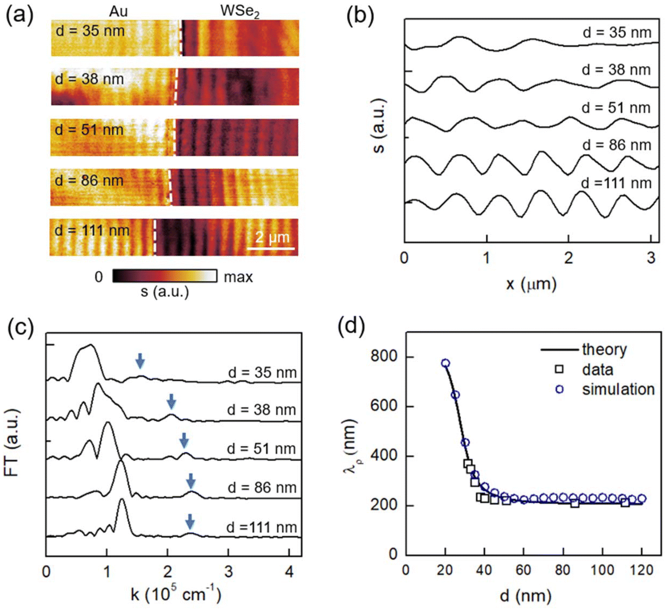
Finally, we wish to explore the dependence of the EPP mode on the thickness of the WSe2 flake (d). In Fig. 3a, we plot the near-field amplitude images taken at E = 1.38 eV from WSe2/Au heterostructures with various WSe2 thicknesses. We found that the bright fringes are sensitively dependent on d. We then extracted the line profiles across the fringes and performed Fourier analysis. In Fig. 3b and c, we plot the fringe profiles and the corresponding FT profiles respectively, based on which we obtained the EPP wavelength with eqn (1). The d-dependent λp from the fringe analysis is plotted in Fig. 3d, which agrees with the theoretical calculations and finite-element simulations (see discussions below). From Fig. 3d, we found that λp decreases rapidly with increasing WSe2 thicknesses for d ≤ 40 nm. As d increases to 50 nm and above, λp approaches ∼210 nm, which is less than a quarter of the free-space photon wavelength. Such high spatial confinement is rarely seen in other polaritonic or plasmonic modes in the near-IR frequency range. The EPP wavelength becomes less sensitive on d for WSe2 flakes thicker than 50 nm.
 |
| | Fig. 3 (a) The near-field amplitude images of WSe2/Au heterostructure waveguides with various WSe2 thicknesses (d). The excitation energy was set to be E = 1.38 eV. (b) The fringe profiles (background subtracted) extracted from near-field images in panel (a). (c) Fourier-transform of the fringe profiles in panel (b). The arrows mark the peak associated with EPP interference involving beam paths ‘P1’ and ‘P2’. (d) The EPP wavelengths as a function of WSe2 thickness from theoretical calculations (curve), experimental data (squares), and finite-element simulations (circles). | |
To understand the thickness dependence of λp (Fig. 3d), we performed finite-element simulations of the EPP mode at E = 1.38 eV with COMSOL Multiphysics. As sketched in Fig. 4a, we constructed the air/WSe2/Au/Si four-layer heterostructure model. The EPPs are launched from left to right along the x axis (marked with an arrow in Fig. 4a). In Fig. 4b, we plot the simulated Ez field maps of the EPP mode for WSe2 with different thicknesses. When the thickness of WSe2 is very small (e.g., d ≤ 20 nm), the polariton field is mainly inside the air. As d increases, the polariton field is confined more and more inside WSe2 resulting in strong light–matter interactions. As a result, λp decreases systematically with increasing WSe2 thickness. For d ≥ 50 nm, the polariton field is localized completely inside WSe2, thus enabling the highest spatial confinement. Further increase of the WSe2 thickness does not significantly affect the field distribution and hence the polariton wavelength.
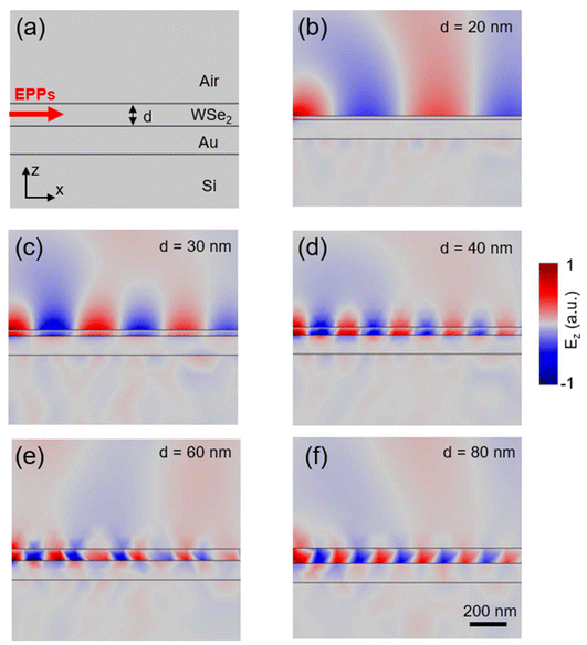 |
| | Fig. 4 (a) Sketch of the air/WSe2/Au/SiO2 four-layer heterostructure model for EPP simulations. (b)–(f) The simulated Ez field maps of the EPP mode inside the WSe2/Au heterostructure with various WSe2 thicknesses. The excitation energy is E = 1.38 eV. | |
Conclusions
In summary, we have performed a comprehensive nano-optical study of the hybrid EPP modes at the WSe2/Au interface, which were formed due to the strong coupling between SPPs on gold and excitons in WSe2. By imaging and analyzing the interference patterns of the EPPs, we were able to determine their wavelengths and construct the dispersion diagram. In addition, we found the EPP wavelength decreases systematically as WSe2 thickness increases, which is due to the stronger localization of the polariton field inside WSe2. The ultimate polariton confinement can be achieved as WSe2 thickness reaches 50 nm and above, where the EPP wavelength is as low as ∼210 nm. Compared to waveguide EPs,20–22 the EPP mode imaged here at the TMD/metal interface is significantly higher confined in space with stronger field enhancement. Both merits are important in technological applications such as on-chip nanophotonic signal processing31 and bio-sensing,32 where devices with small footprints and high sensitivity are desirable.
Conflicts of interest
There are no conflicts to declare.
Acknowledgements
This work was supported by the U.S. Department of Energy (DOE), Office of Science, Basic Energy Sciences, Materials Science and Engineering Division. The research was performed at Ames Laboratory, which is operated for the U.S. DOE by Iowa State University under contract # DE-AC02-07CH11358.
References
- J. Bellessa, C. Symonds, C. Meynaud, J. C. Plenet, E. Cambril, A. Miard, L. Ferlazzo and A. Lemaître, Phys. Rev. B: Condens. Matter Mater. Phys., 2008, 78, 205326 CrossRef.
- M. Rödel, P. Lisinetskaya, M. Rudloff, T. Startk, J. Manara, R. Mitric and J. Pflaum, J. Phys. Chem. C, 2022, 126, 4163–4171 CrossRef.
- P. Törmä and W. L. Barnes, Rep. Prog. Phys., 2015, 78, 013901 CrossRef PubMed.
- A. Berrier, R. Cools, C. Arnold, P. Offermans, M. Crego-Calama, S. H. Brongersma and J. Gómez-Rivas, ACS Nano, 2011, 5, 6226–6232 CrossRef CAS PubMed.
- N. Lundt, S. Klembt, E. Cherotchenko, S. Betzold, O. Iff, A. V. Nalitov, M. Klaas, C. P. Dietrich, A. V. Kavokin, S. Höfling and C. Schneider, Nat. Commun., 2016, 7, 13328 CrossRef CAS PubMed.
- B. Lee, W. Liu, C. H. Naylor, J. Park, S. C. Malek, J. S. Berger, A. T. C. Johnson and R. Agarwal, Nano Lett., 2017, 17, 4541–4547 CrossRef CAS PubMed.
- P. Vasa, R. Pomraenke, S. Schwieger, Y. I. Mazur, V. Kunets, P. Srinivasan, E. Johnson, J. E. Kihm, D. S. Kim, E. Runge, G. Salamo and C. Lienau, Phys. Rev. Lett., 2008, 101, 116801 CrossRef CAS PubMed.
- P. Ni, A. D. L. Bugallo, V. M. A. Arreola, M. F. Salazar, E. Strupiechonski, V. Brandli, R. Sawant, B. Alloing and P. Genevet, ACS Photonics, 2019, 6, 1594–1601 CrossRef CAS.
- R. K. Chowdhury, P. K. Datta, S. N. B. Bhaktha and S. K. Ray, Adv. Opt. Mater., 2020, 8, 1901645 CrossRef CAS.
- H. Zhang, B. Abhiraman, Q. Zhang, J. Miao, K. Jo, S. Roccasecca, M. W. Knight, A. R. Davoyan and D. Jariwala, Nat. Commun., 2020, 11, 3552 CrossRef CAS PubMed.
- E. Cao, W. Lin, M. Sun, W. Liang and Y. Song, Nanophotonics, 2018, 7, 145–167 Search PubMed.
- C. Weisbuch, M. Nishioka, A. Ishikawa and Y. Arakawa, Phys. Rev. Lett., 1992, 69, 3314–3317 CrossRef CAS PubMed.
- H. M. Gibbs, G. Khitrova and S. W. Koch, Nat. Photonics, 2011, 5, 273 CrossRef.
- F. Tassone, F. Bassani and L. C. Andreani, Phys. Rev. B: Condens. Matter Mater. Phys., 1992, 45, 6023–6030 CrossRef PubMed.
- H. Deng, H. Haug and Y. Yamamoto, Rev. Mod. Phys., 2010, 82, 1489–1537 CrossRef CAS.
- D. N. Basov, M. M. Fogler and F. J. García de Abajo, Science, 2016, 354, 6309 CrossRef PubMed.
- T. Low, A. Chaves, J. D. Caldwell, A. Kumar, N. X. Fang, P. Avouris, T. F. Heinz, F. Guinea, L. Martin-Moreno and F. Koppens, Nat. Mater., 2017, 16, 182–184 CrossRef CAS PubMed.
- X. Liu, T. Galfsky, Z. Sun, F. Xia, E.-C. Lin, Y.-H. Lee, S. Kéna-Cohen and V. M. Menon, Nat. Photonics, 2015, 9, 30–34 CrossRef CAS.
- S. Dufferwiel, S. Schwarz, F. Withers, A. A. P. Trichet, F. Li, M. Sich, O. Del Pozo-Zamudio, C. Clark, A. Nalitov, D. D. Solnyshkov, G. Malpuech, K. S. Novoselov, J. M. Smith, M. S. Skolnick, D. N. Krizhanovskii and A. I. Tartakovskii, Nat. Commun., 2015, 6, 8579 CrossRef CAS PubMed.
- F. Hu, Y. Luan, M. E. Scott, J. Yan, D. G. Mandrus, X. Xu and Z. Fei, Nat. Photonics, 2017, 11, 356–360 CrossRef CAS.
- F. Hu, Y. Luan, J. Speltz, D. Zhong, C. H. Liu, J. Yan, D. G. Mandrus, X. Xu and Z. Fei, Phys. Rev. B, 2019, 100, 121301(R) CrossRef.
- Y. Luan, H. Zobeiri, X. Wang, E. Sutter, P. Sutter and Z. Fei, Nano Lett., 2022, 22, 1497–1503 CrossRef CAS PubMed.
- N. Saigal, V. Sugunakar and S. Ghosh, Exciton binding energy in bulk MoS2: A reassessment, Appl. Phys. Lett., 2016, 108, 132105 CrossRef.
- A. Chernikov, T. C. Berkelbach, H. M. Hill, A. Rigosi, Y. Li, O. B. Aslan, D. R. Reichman, M. S. Hybertsen and T. F. Heinz, Phys. Rev. Lett., 2014, 113, 076802 CrossRef CAS PubMed.
- K. He, N. Kumar, L. Zhao, Z. Wang, K. F. Mak, H. Zhao and J. Shan, Phys. Rev. Lett., 2014, 113, 026803 CrossRef CAS PubMed.
- A. T. Hanbicki, M. Currie, G. Kioseoglou, A. L. Friedman and B. T. Jonker, Solid State Commun., 2015, 203, 16–20 CrossRef CAS.
- A. R. Beal, W. Y. Liang and H. P. Hughes, J. Phys. C: Solid State Phys., 1976, 9, 2449–2457 CrossRef CAS.
- M. Mrejen, L. Yadgarov, A. Levanon and H. Suchowski, Sci. Adv., 2019, 5, eaat9618 CrossRef CAS PubMed.
- D. Hu, X. Yang, C. Li, R. Liu, Z. Yao, H. Hu, S. N. G. Corder, J. Chen, Z. Sun, M. Liu and Q. Dai, Nat. Commun., 2017, 8, 1471 CrossRef PubMed.
- A. J. Sternbach, S. Latini, S. Chae, H. Hübener, U. D. Giovannini, Y. Shao, L. Xiong, Z. Sun, N. Shi, P. Kissin, G.-X. Ni, D. Rhodes, B. Kim, N. Yu, A. J. Millis, M. M. Fogler, P. J. Schuck, M. Lipson, X.-Y. Zhu, J. Hone, R. D. Averitt, A. Rubio and D. N. Basov, Nat. Commun., 2020, 11, 3567 CrossRef CAS PubMed.
- Y. Fang and M. Sun, Light: Sci. Appl., 2015, 4, e294 CrossRef CAS.
- S.-H. Oh, H. Altug, X. Jin, T. Low, S. J. Koester, A. P. Ivanov, J. B. Edel, P. Avouris and M. S. Strano, Nat. Commun., 2021, 12, 3824 CrossRef CAS PubMed.
|
| This journal is © The Royal Society of Chemistry 2022 |

 Open Access Article
 This Open Access Article is licensed under a Creative Commons Attribution-Non Commercial 3.0 Unported Licence
 ab,
Yilong
Luan
ac,
Ruth
Shinar
ab,
Yilong
Luan
ac,
Ruth
Shinar