DOI:
10.1039/D2NR04119G
(Paper)
Nanoscale, 2022,
14, 14537-14543
Single charge control of localized excitons in heterostructures with ferroelectric thin films and two-dimensional transition metal dichalcogenides†
Received
26th July 2022
, Accepted 20th September 2022
First published on 20th September 2022
Abstract
Single charge control of localized excitons (LXs) in two-dimensional transition metal dichalcogenides (TMDCs) is crucial for potential applications in quantum information processing and storage. However, traditional electrostatic doping method by applying metallic gates onto TMDCs may cause inhomogeneous charge distribution, optical quenching, and energy loss. Herein, by locally controlling the ferroelectric polarization of the ferroelectric thin film BiFeO3 (BFO) with a scanning probe, we can deterministically manipulate the doping type of monolayer WSe2 to achieve p-type and n-type doping. This nonvolatile approach can maintain the doping type and hold the localized excitonic charges for a long time without applied voltage. Our work demonstrated that the ferroelectric polarization of BFO can control the charges of LXs effectively. Neutral and charged LXs have been observed in different ferroelectric polarization regions, confirmed by magnetic optical measurement. Highly circular polarization degree with 90% photon emission from these quantum emitters was achieved in high magnetic fields. Controlling the single charge of LXs in a non-volatile way shows a great potential for deterministic photon emission with desired charge states for photonic long-term memory.
Introduction
High-quality quantum light sources are highly desired to implement quantum key distribution and linear optical quantum computation for information processing.1–5 Solid-state quantum emitters have attracted more attention because of their addressability and integrability. Many solid-state single-photon sources are based on confined low dimensional materials, including nitrogen vacancies in diamond and semiconductor quantum dots.6–9 Recently, nonclassical quantum emissions have been observed in semiconductor transition metal dichalcogenides (TMDCs), which were ascribed to LXs introduced by the point defects or electronic perturbations in the monolayer TMDCs.6,10–15 By intentionally introducing local strains, these quantum emitters can be site-controlled and arrayed.16–18 Quantum emitters in tungsten-based TMDCs systems have been investigated in many studies.6,12,19 For example, in WSe2, single photon sources have been demonstrated from the intervalley defect excitons associated with the hybridization of dark excitons by point-like strain perturbations or vacancies.20–22
Since atomically thin layers of TMDCs can be stacked vertically using a simple mechanical exfoliation method, quantum emitters can be integrated into a range of functional heterostructure devices, which makes electrical charge control possible.23,24 Recently, LXs have been studied in vertically assembled heterostructures using gated electrostatic doping.25,26 The electric field was used to tune the band energy of quantum emitters by the Stark effect and control the fine structure splitting (FSS) by exciton wave function modulation.27,28 Normally, neutral LXs at zero magnetic field possess FSS with orthogonal linear polarizations caused by electron–hole exchange interactions. In contrast, charged LXs do not have FSS due to the disappearance of exchange interactions by the excess electrons or holes.29,30 Therefore, the deterministic control of the charge state of LXs is essential to realize desired exciton recombination.
Typically, the charge density of TMDCs can be controlled by gate-bias tuning.29,31,32 In this way, a transverse p–n junction has been demonstrated by controlling the gate voltage. However, the metal gate would result in inhomogeneous charge distribution and direct contact between the metal, and the monolayer TMDCs would also lead to an optical quenching. When the gate voltage is removed, the charge density cannot be maintained. To overcome these, integrating ferroelectric films (FE) with TMDCs provides a strategy for controlling the charge of the LXs since the spontaneous polarization of FE can be reversed with external stimuli, and can keep the ferroelectric polarization for a long time.33–35 In addition, the TMDCs/FE heterostructure largely eliminates interface problems introduced by electrode contacts.36,37 Using scanning probe technique, ferroelectric domains with good retention can be formed with TMDCs in a non-volatile manner, allowing the design of devices not limited by physical source, drain, and gate electrodes.36 The integrated heterostructures could also provide a way for the seamless integration of data processing and storage.38
In this work, a 10% Zn-doped BFO ferroelectric thin film and a monolayer WSe2 were used to build a gate-free heterostructure WSe2/BFO, with which the carrier doping of WSe2 could be controlled by the ferroelectric polarization of BFO. We demonstrate that the carrier doping of WSe2 in the downward polarization (Pdown) region is p-type, while in the upward polarization (Pup) region, it is n-type at room temperature. At low temperature without a magnetic field, the photoluminescence (PL) peaks of LXs are mostly doublets at the domain wall, while the singlets are mainly located in the Pdown and Pup regions. The lack of FSS is a feature of charged LXs,29,30 while neutral LXs are more likely to be produced at the domain wall. The presence of charged and neutral LXs is further confirmed by magneto-optical measurements. Highly circular polarization of PL of about 90% from quantum emitters is observed under a high magnetic field. Using electrical polarization of BFO, controlling the single charges of LXs provides a method for achieving quantum emitters with desired charging states in a non-volatile way.
Results and discussion
Scanning probe microscopy
A schematic plot of the WSe2/BFO heterostructure is shown in Fig. 1(a), and the fabrication process is summarized in the Methods section. The BFO film was grown on 20 nm strontium ruthenate (SRO)-buffered (001) strontium titanate (STO) substrates. Mechanical exfoliation and dry transfer were used to create the van der Waals interface of WSe2/BFO. The optical microscopy images of the monolayer WSe2 before and after the transfer are shown in ESI (Fig. S1†). The atomic force microscopy (AFM) image is shown in Fig. 1(b). The orange line in Fig. 1(e) shows that the thickness of WSe2 is about 1 nm, indicating a monolayer, which is also consistent with Raman and PL results at room temperature (as presented in ESI Fig. S2†). The ferroelectric polarization of BFO can be reversed by applying a voltage.34 The piezoelectric force microscopy (PFM) image of the WSe2/BFO heterostructure is presented in Fig. 1(c). The Zn-doping BFO film exhibits distinct downward polarization (Pdown) self-poling polarization in the white box region and perfect polarization-voltage (P–V) loop with a large remanent polarization value ∼60 μC cm−2 (as shown in Fig. 1(d)). In order to obtain an upward polarization (Pup) region, we applied a −15 V voltage at the metal probe to reverse the downward polarization of the BFO film. As shown by the green line in Fig. 1(e), the out-of-plane PFM phase of BFO is different by about 180° between the Pup and Pdown regions, confirming that the polarization direction can be effectively switched by the external electric field. The upper surface of the BFO is rich with positive charges in the Pup region, and the opposite is true in the Pdown region. The junction between Pdown and Pup is the domain wall, labelled as Pdw. The domain wall is at the boundary of positive and negative charges; thus, it is possible to form a neutral environment. The geometry of the monolayer WSe2 in the PFM image matches that of the AFM image, indicating that the monolayer WSe2 was not damaged during polarization reversal with applied voltage.
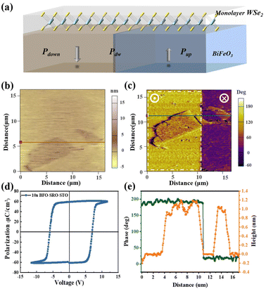 |
| | Fig. 1 The ferroelectric properties of BFO and the scanning probe microscopic images of WSe2/BFO. (a) A schematic plot of the WSe2/BFO heterostructure. (b and c) AFM and PFM images of WSe2/BFO. The yellow region represents the Pup region, and the violet region represents the Pdown region. (d) Electric P–V hysteresis loops. The BFO film has a dramatic ferroelectric switch, and its remanent polarization is about 60 μC cm−2. (e) The thickness of monolayer WSe2 measured along the solid orange line in (b) and out-of-plane PFM phase of BFO along the green solid line in (c). The thickness of monolayer WSe2 is approximately 1 nm. The out-of-plane PFM phase of BFO is different by about 180° in the Pup and Pdown regions. | |
Photoluminescence spectra at zero magnetic field
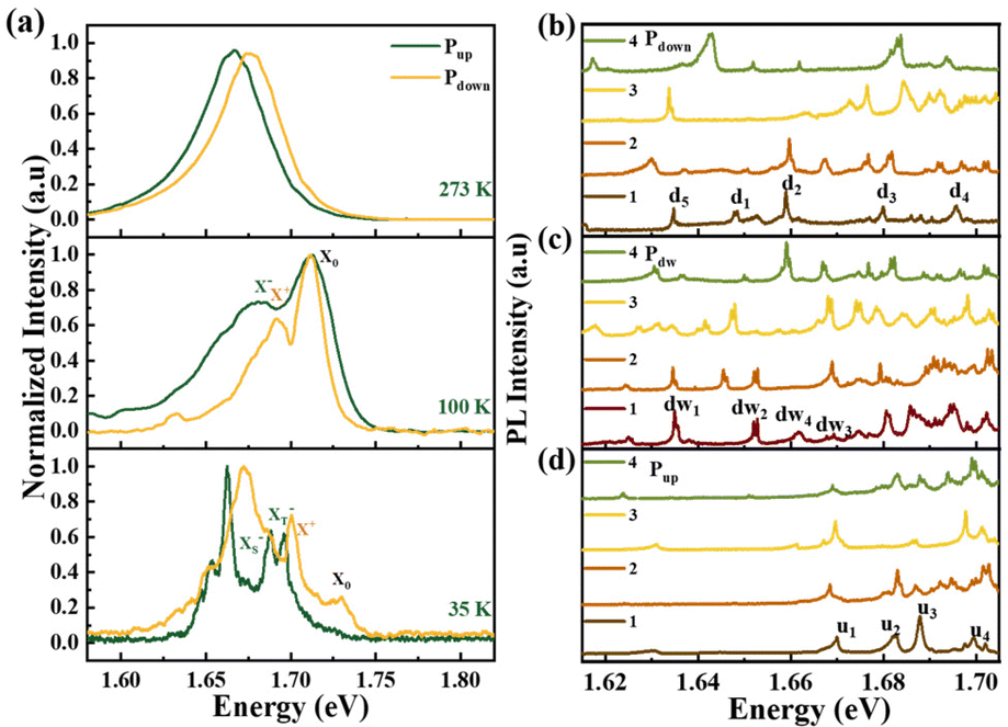
To elucidate the role of the ferroelectric nature of BFO on the charge density of monolayer WSe2, the temperature-dependent PL measurements were performed from 35 K to 273 K, as shown in Fig. 2(a). Because of the large binding energy and direct band gap of monolayer TMDCs, direct band recombination with different type of carrier doping can be resolved by PL spectroscopy even at room temperature.39,40 Unlike the intrinsic exciton (Xin), the localized exciton is quickly quenched as the temperature rises. The emission of 1.73 eV at 35 K corresponds to the neutral exciton X0. The energy difference between the neutral and charged excitons allows us to determine the carrier doping type of the device. In the Pup region, two different trions states of negatively charged exciton (Xin−) are located at 1.688 eV and 1.696 eV under 35 K, which correspond to the triplet trion (XinT−) and the singlet trion (XinS−). On the other hand, in the Pdown region, the positively charged exciton Xin+ is singlet state.41–44 The emission of negatively charged intrinsic exciton Xin− in the Pup region is red-shifted by about 10 meV relative to the Xin+ in the Pdown region at low temperature. The PL from Pup region also undergoes a red-shift of about 15 meV at 273 K, which is consistent with previous reports on PL with metal electrostatic gating.41–44 This demonstrates that the direct bandgap recombination of WSe2 switched from positively charged excitons to negatively charged excitons from the natural downward polarization Pdown region to the polarization flipped Pup region. The g-factors of intrinsic excitons in the Pdown and Pup regions are extracted with polarization-resolved magneto-PL at 4.2 K (as shown in ESI Fig. S3†). The g-factors in the two regions are both close to 4, further confirming that they are direct band gap emissions.12,42,44–47
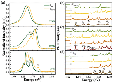 |
| | Fig. 2 PL spectra at zero magnetic field. (a) Temperature-dependent PL spectra from 35 K to 273 K in the Pdown and Pup regions. (b–d) PL spectra under different positions of the Pdown region (a), the Pdw region (b), and the Pup region (c) at 4.2 K. | |
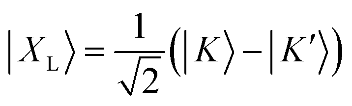
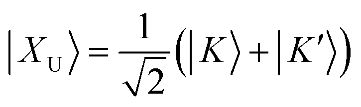
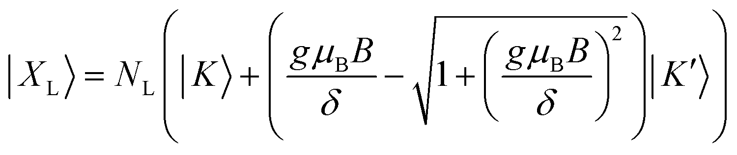
Fig. 2(b–d) depict the PL spectra of monolayer WSe2 at different positions in the three regions of Pdown, Pup, and Pdw at 4.2 K. As shown in Fig. 1c, the WSe2 flake is approximately 3 μm at the junction, which is large enough to avoid lateral confinement effects. Many narrow peaks were observed in the low-energy region, and the full widths at half maximum of these peaks fall between 100 and 500 μeV. We attribute these peaks to the localized single exciton transitions induced by the interaction or combination of crystal defects and local strain during the transfer process. Compared with the Xin, the LXs have a narrower linewidth and lower energy. Intriguingly, the PL peaks of these LXs exhibit different characteristics at the zero magnetic field, some of which are doublets and others are only single peaks (singlets). The PL peaks of LXs located at the domain wall are mainly doublets and the two peaks have cross-linearly polarized emission (as shown in ESI Fig. S4†), which indicates that the doublets at the domain wall originate from the same localized exciton. The splitting is the result of FSS caused by anisotropic electron–hole exchange interactions in asymmetric confinement potentials.48,49 However, in our experiments, singlets are mainly observed in the Pdown and Pup regions. Due to the ferroelectric polarization of BFO, the density of negative charges in monolayer WSe2 increases in the Pup region, making it easier to produce negatively charged excitons (X−), while the positively charged excitons (X+) in the Pdown region are increased. The charged exciton at its lowest energy state consists of two holes (electrons) with opposite spins and one electron (hole).26,29,50,51
Magneto photoluminescence spectra measurements
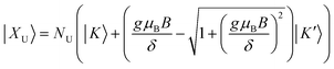
To further investigate the magnetic optical properties of LXs, the magneto-PL measurements were performed in three regions of Pdown, Pup, and Pdw. Fig. 3 shows the magnetic response of the labeled PL peaks of LXs in Fig. 2(b–d). The typical X-shaped dispersion can be observed in all the three regions. The FSSs at zero magnetic field of the doublets in all the three regions are approximately 700–800 μeV, which are consistent with the previously reported values.52,53 The emission of the LXs at zero magnetic field is linearly polarized. This is because the monolayer WSe2 valley degrees of freedom and spin degrees of freedom are locked, then the eigenstates at zero magnetic field are a linear superposition of the left-hand circularly polarized excitonic state |K〉 and the right-hand circularly polarized excitonic state |K′〉, and they have equal weights.54| | 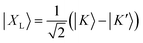 | (1) |
| |  | (2) |
 |
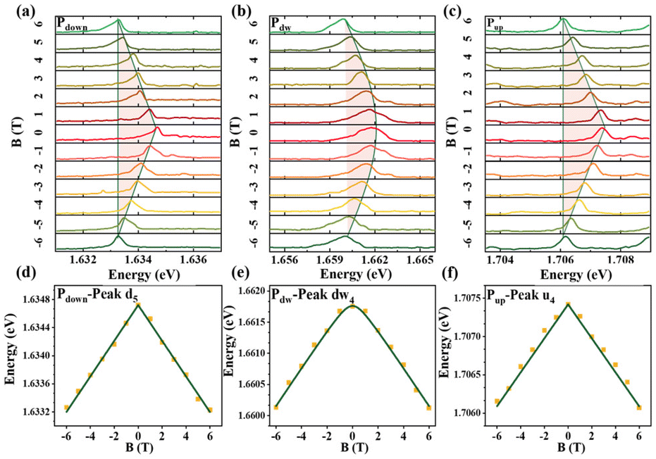
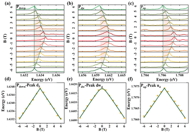
| | Fig. 3 Magneto-PL in Pdown, Pup, and Pdw regions by applying a Faraday configuration magnetic field (perpendicular to the sample). Contour plots of PL spectra as a function of magnetic field in different regions, Pdown (a), Pdw (b), and Pup (c). (d–f) Energy splitting as a function of the applied magnetic field. The solid lines represent the fitting of experimental data. Peak d2, d3, and d4 in the Pdown (d) region are singlets with g-factors of 9.93, 9.84, and 9.97, respectively. Peak d1 is a doublet with g-factor and FSS values of 9.01 and 703.1 μeV, respectively. Peak dw1, dw2, and dw3 in the Pdw region (e) have g-factors and FSSs of 9.02, 9.41, 9.65 and 692.01, 708.96, and 882.02 μeV, respectively. The g-factors of peak u1, u2, and u3 in the Pup region (f) are 10.22, 10.43, and 10.27, respectively, and the FSS of peak u2 is 735.02 μeV. | |
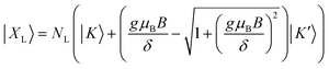
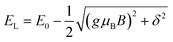
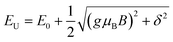
As the magnetic field increases, the degeneracy is gradually lifted.
| |  | (3) |
| |  | (4) |
| |  | (5) |
| |  | (6) |
where
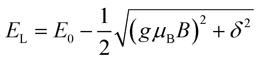
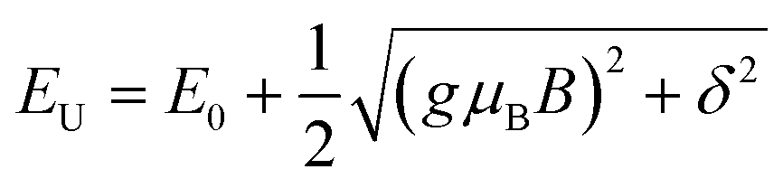
L refers to the low energy peak, while
U denotes the high energy peak,
μB is the Boltzmann constant,
g represents the Landé factor,
δ denotes the FSS at zero field, and
NL and
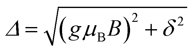
NU are magnetic field dependent normalization constants. The energy splitting (
Δ) between high energy peak and low energy peak as a function of applied magnetic field is shown in
Fig. 3(d–f). For doublets, we extract the exciton
g-factor using the expression.
| |  | (7) |
In contrast to the behaviors of doublets at low magnetic fields, in which the energy splitting increases quadratically with the magnetic field, the energy splitting of the singlets in Pdown and Pup is a linear function of magnetic field due to the absence of zero field FSS.
| |  | (8) |
The g-factors of singlets (peak d2, d3, and d4) in the Pdown region are 9.93, 9.84, and 9.97, and those in the Pup region (peak u1 and u3) are 10.43 and 10.27, respectively. The g-factors of all the doublets in all the three regions are approximately 9.30. It is consistent with the previous reports on the g-factor for LXs of monolayer WSe2.10,51 This is because ferroelectric polarization affects the charge level of monolayer WSe2, leading to the production of positively charged LXs in the Pdown region and negatively charged LXs in the Pup region. On the other hand, carrier distribution induced by the domain wall provides more opportunities to generate neutral LXs.
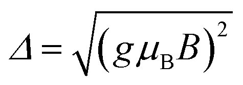
Unlike the PL peaks of LXs in Fig. 3 with distinct Zeeman splitting, we also found several PL peaks whose high energy branch component is strongly suppressed over the entire magnetic field range. As displayed in Fig. 4(a–c), the PL peak shifts into the low energy direction as the magnetic field increases, while the high energy branch component is unresolved. Fig. 4(d–f) illustrate the variation of the energy with increasing magnetic field. For peak dw4 in the Pdw region, the variation curve of energy with magnetic field is parabolic, whereas the peak d5 in Pdown and peak u4 in Pup are straight lines. The solid line represents the fitting by eqn (5), from which we can extract the g-factor and zero field FSS. The g-factors of peak d5, peak dw4, and peak u4 are 8.76, 10.60, and 7.65, respectively. The zero field FSS values cannot be extracted for peak d5 and peak u4 in Pdown and Pup regions. The lack of zero field FSS is the hallmark of charged LXs. This matches well with the results we discussed earlier that the charged LXs were generated in the Pdown and Pup regions via the charge control of WSe2 by the ferroelectric polarization of BFO. On the other hand, for peak dw4 in the Pdw region, a zero field FSS of 497.23 μeV can be obtained, which is a little smaller than the reported value of WSe2.10,51 The missing of the high energy branch in the magnetic spectrum can be explained by two reasons. One is thermal relaxation, with which carriers preferably occupy the lower energy levels.6,26,55,56 Second, strong asymmetry might induce the high energy branch with a small optical oscillator strength.10,54 In our experiment, the strong asymmetry of the confining potential might be induced by the unevenness of the substrate or wrinkling during the transfer process.
 |
| | Fig. 4 Magneto-PL of peak d5, dw4, and u4 by applying a Faraday configuration magnetic field. (a–c) Magneto-PL spectra of the peak d5 (a), peak dw4 (b), and peak u4 (c). (d–f) Energy as a function of the applied magnetic field. The solid lines represent the data fitted by eqn (5) and (6). g-factor of peak d5 in the Pdown region is 8.76 (d), peak u4 in the Pup region is 7.65 (f). For peak dw4 in Pdw region, the g factor of 10.60 and FSS of 497.23 μeV are extracted. | |
Polarization-resolved magneto photoluminescence spectra measurements
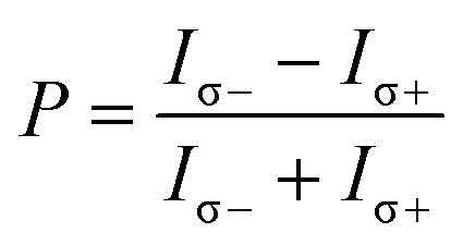
According to the eqn (1)–(4), the circular polarization degree of LXs increases with magnetic field increasing. Fig. 5(a and b) depict the circularly polarized PL spectra of peak u4 with a linearly polarized excitation. The PL intensity of σ− emission is significantly higher than that of σ+ with a positive magnetic field, while σ+ emission is much stronger for a negative magnetic field. Fig. 5(c) illustrates the degree of circular polarization degree extracted from the integral intensity of PL peaks. The degree of circular polarization is defined as| |  | (9) |
where Iσ+ (Iσ−) denotes the intensity of the σ+ (σ−) polarized emissions excited with linearly polarized light. The peak u4 goes from linearly polarized at zero magnetic field to gradually circularly polarized as the magnetic field increases. When the magnetic field strength reaches 6 T, the circular polarization degree of 90% can be obtained, as shown in Fig. 5(c), which is close to the experimental results of single self-assembled quantum dots.48 The circular polarization degrees of other similar LXs are presented in ESI Fig. S5.†
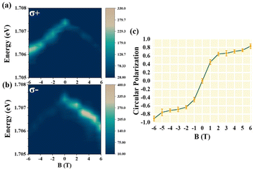 |
| | Fig. 5 Contour plot of polarization-resolved magneto-PL peak u4 in a Faraday configuration magnetic field. (a and b) Polarization-resolved magneto-PL under linearly polarized excitation for σ+ (a) and σ− (b) collection. (c) The circular polarization degree of the lower energy branch of peak u4 obtained from (a) and (b). | |
Methods
Device fabrication
To fabricate WSe2/BFO heterojunction, the Bi1.3Fe0.9Zn0.1O3 films were grown firstly on ∼20 nm strontium ruthenate (SRO)-buffered (001) strontium titanate (STO) substrates with a laser molecular beam epitaxy system. The WSe2 monolayer films on scotch tape was prepared by the mechanical exfoliation method. The monolayer was then transferred onto the BFO film using PDMS as a transfer medium, resulting in a heterostructure. AFM and PFM characterization was done a commercial AFM system (Asylum Research, MFP-3D). Ti/Pt coated silicon probes with a tip radius of about 28 nm were used for collecting and recording the PFM images.
PL measurement
The samples were placed on a three-dimensional piezoelectric stage with a superconducting magnet cryostat, in which a vertical magnetic field of ±9 T and a low temperature of 4.2 K can be provided. All PL measurements were performed using a confocal microscope system. A large numerical aperture objective lens of 0.82 was used to excite the sample and collect PL light. The sample was excited with a continuous wave 532 nm laser. The PL signal was coupled into a single-mode fiber and acquired through a grating spectrometer with a liquid nitrogen-cooled charge-coupled device.
Conclusion
We have demonstrated successfully that the ferroelectric polarization of BFO can control the single charges of LXs of monolayer WSe2 with WSe2/BFO heterojunction. Ferroelectric gating can maintain the charges of exciton for a long time in a non-volatile and low-energy manner. The doping type of direct bandgap emission of WSe2 changes from n-type to p-type, which was confirmed from the Pdown region to the Pup region with PL peak energy shifting at different temperatures. For LXs, the singlet with the absence of FSS in Pdown and Pup regions is attributed to the extra charge introduced by the ferroelectric polarization. Most neutral LXs have been observed in the Pdw region at the domain walls, which is confirmed with magneto-PL measurements. Moreover, a high circular polarization with 90% LXs was obtained at a high magnetic field of 6T. Singly charge state control in LXs in TMDCs with the FE substrate provides a method for long-term single spin detection and spin storage in a non-volatile manner, which could be useful for TMDCs-based information processing. In this work, the domination of zero-field FSS at the domain walls indicates the polarization confinement, which lays the groundwork for the physical exploration of the role of polarization confinement at the domain walls on localized excitons.
Author contributions
X. Xu, C.W., K. J. and Q. G. conceived and planned the project. D. D and X. W fabricated the devices. D. D., J. Y., J. D., Y. Y., B. F., X. Xie, L. Y., S. X., S. S., S. Y., R. Z. and Z. Z. performed the optical measurement. All authors discussed the results and wrote the manuscript.
Conflicts of interest
The authors declare no competing interests.
Acknowledgements
This work was supported by the National Key Research and Development Program of China (Grant No. 2021YFA1400700), the National Natural Science Foundation of China (Grants No. 62025507, 11934019, 11721404, 11874419, 62175254 and 12174437), the Key R&D Program of Guangdong Province (Grant No. 2018B030329001), the Strategic Priority Research Program (Grant No. XDB28000000) of the Chinese Academy of Sciences.
References
- M. Turunen, M. Brotons-Gisbert, Y. Dai, Y. Wang, E. Scerri, C. Bonato, K. D. Jöns, Z. Sun and B. D. Gerardot, Nat. Rev. Phys., 2022, 4, 219–236 CrossRef.
- A. K. Ekert, Phys. Rev. Lett., 1991, 67, 661–663 CrossRef PubMed.
- J. L. O'Brien, A. Furusawa and J. Vučković, Nat. Photonics, 2009, 3, 687–695 CrossRef.
- K. A. Patel, J. F. Dynes, I. Choi, A. W. Sharpe, A. R. Dixon, Z. L. Yuan, R. V. Penty and A. J. Shields, Phys. Rev. X, 2012, 2, 041010 CAS.
- P. Senellart, G. Solomon and A. White, Nat. Nanotechnol., 2017, 12, 1026–1039 CrossRef CAS.
- Y. M. He, G. Clark, J. R. Schaibley, Y. He, M. C. Chen, Y. J. Wei, X. Ding, Q. Zhang, W. Yao, X. Xu, C. Y. Lu and J. W. Pan, Nat. Nanotechnol., 2015, 10, 497–502 CrossRef CAS.
- C. M. Kurtsiefer, S. Mayer, P. Zarda and H. Weinfurter, Phys. Rev. Lett., 2000, 85, 290–293 CrossRef CAS PubMed.
- B. M. Lounis and W. E. Moerner, Nature, 2000, 407, 491–493 CrossRef CAS PubMed.
- P. Michler, Science, 2000, 290, 2282–2285 CrossRef CAS PubMed.
- C. Chakraborty, L. Kinnischtzke, K. M. Goodfellow, R. Beams and A. N. Vamivakas, Nat. Nanotechnol., 2015, 10, 507–511 CrossRef CAS PubMed.
- T. T. Tran, K. Bray, M. J. Ford, M. Toth and I. Aharonovich, Nat. Nanotechnol., 2016, 11, 37–41 CrossRef CAS PubMed.
- M. Koperski, K. Nogajewski, A. Arora, V. Cherkez, P. Mallet, J. Y. Veuillen, J. Marcus, P. Kossacki and M. Potemski, Nat. Nanotechnol., 2015, 10, 503–506 CrossRef CAS PubMed.
- S. Sun, Y. Yu, J. Dang, K. Peng, X. Xie, F. Song, C. Qian, S. Wu, H. Ali, J. Tang, J. Yang, S. Xiao, S. Tian, M. Wang, X. Shan, M. A. Rafiq, C. Wang and X. Xu, Appl. Phys. Lett., 2019, 114, 113104 CrossRef.
- Y. Yu, J. Dang, C. Qian, S. Sun, K. Peng, X. Xie, S. Wu, F. Song, J. Yang, S. Xiao, L. Yang, Y. Wang, X. Shan, M. A. Rafiq, B.-B. Li and X. Xu, Phys. Rev. Mater., 2019, 3, 051001 CrossRef CAS.
- J. Dang, M. Yang, X. Xie, Z. Yang, D. Dai, Z. Zuo, C. Wang, K. Jin and X. Xu, Small, 2022, 18, e2106029 CrossRef.
- J. Klein, M. Lorke, M. Florian, F. Sigger, L. Sigl, S. Rey, J. Wierzbowski, J. Cerne, K. Muller, E. Mitterreiter, P. Zimmermann, T. Taniguchi, K. Watanabe, U. Wurstbauer, M. Kaniber, M. Knap, R. Schmidt, J. J. Finley and A. W. Holleitner, Nat. Commun., 2019, 10, 2755 CrossRef CAS.
- L. Chirolli, E. Prada, F. Guinea, R. Roldán and P. San-Jose, 2D Mater., 2019, 6, 025010 CrossRef CAS.
- A. M. Jones, H. Yu, N. J. Ghimire, S. Wu, G. Aivazian, J. S. Ross, B. Zhao, J. Yan, D. G. Mandrus, D. Xiao, W. Yao and X. Xu, Nat. Nanotechnol., 2013, 8, 634–638 CrossRef CAS.
- D. Gammon, B. V. Shanabrook and D. S. Katzer, Phys. Rev. Lett., 1991, 67, 1547–1550 CrossRef CAS PubMed.
- L. Linhart, M. Paur, V. Smejkal, J. Burgdorfer, T. Mueller and F. Libisch, Phys. Rev. Lett., 2019, 123, 146401 CrossRef CAS PubMed.
- S. Zhang, C. G. Wang, M. Y. Li, D. Huang, L. J. Li, W. Ji and S. Wu, Phys. Rev. Lett., 2017, 119, 046101 CrossRef PubMed.
- Y. J. Zheng, Y. Chen, Y. L. Huang, P. K. Gogoi, M. Y. Li, L. J. Li, P. E. Trevisanutto, Q. Wang, S. J. Pennycook, A. T. S. Wee and S. Y. Quek, ACS Nano, 2019, 13, 6050–6059 CrossRef CAS PubMed.
- G. Plechinger, P. Nagler, A. Arora, R. Schmidt, A. Chernikov, A. G. Del Aguila, P. C. Christianen, R. Bratschitsch, C. Schuller and T. Korn, Nat. Commun., 2016, 7, 12715 CrossRef CAS PubMed.
- C. Jin, E. C. Regan, A. Yan, M. Utama, D. Wang, S. Zhao, Y. Qin, S. Yang, Z. Zheng, S. Shi, K. Watanabe, T. Taniguchi, S. Tongay, A. Zettl and F. Wang, Nature, 2019, 567, 76–80 CrossRef CAS PubMed.
- C. Chakraborty, L. Qiu, K. Konthasinghe, A. Mukherjee, S. Dhara and N. Vamivakas, Nano Lett., 2018, 18, 2859–2863 CrossRef CAS PubMed.
- X. Lu, X. Chen, S. Dubey, Q. Yao, W. Li, X. Wang, Q. Xiong and A. Srivastava, Nat. Nanotechnol., 2019, 14, 426–431 CrossRef CAS PubMed.
- C. Chakraborty, K. M. Goodfellow, S. Dhara, A. Yoshimura, V. Meunier and A. N. Vamivakas, Nano Lett., 2017, 17, 2253–2258 CrossRef CAS PubMed.
- C. Chakraborty, N. R. Jungwirth, G. D. Fuchs and A. N. Vamivakas, Phys. Rev. B, 2019, 99, 045308 CrossRef CAS.
- M. Brotons-Gisbert, A. Branny, S. Kumar, R. Picard, R. Proux, M. Gray, K. S. Burch, K. Watanabe, T. Taniguchi and B. D. Gerardot, Nat. Nanotechnol., 2019, 14, 442–446 CrossRef CAS PubMed.
- M. Bayer, G. Ortner, O. Stern, A. Kuther, A. A. Gorbunov, A. Forchel, P. Hawrylak, S. Fafard, K. Hinzer, T. L. Reinecke, S. N. Walck, J. P. Reithmaier, F. Klopf and F. Schäfer, Phys. Rev. B: Condens. Matter Mater. Phys., 2002, 65, 19315 Search PubMed.
- J. S. Ross, P. Klement, A. M. Jones, N. J. Ghimire, J. Yan, D. G. Mandrus, T. Taniguchi, K. Watanabe, K. Kitamura, W. Yao, D. H. Cobden and X. Xu, Nat. Nanotechnol., 2014, 9, 268–272 CrossRef CAS PubMed.
- D. Jariwala, V. K. Sangwan, C. C. Wu, P. L. Prabhumirashi, M. L. Geier, T. J. Marks, L. J. Lauhon and M. C. Hersam, Proc. Natl. Acad. Sci. U. S. A., 2013, 110, 18076–18080 CrossRef CAS PubMed.
- S. Tian, C. Wang, Y. Zhou, X. Li, P. Gao, J. Wang, Y. Feng, X. Yao, C. Ge, M. He, X. Bai, G. Yang and K. Jin, ACS Appl. Mater. Interfaces, 2018, 10, 43792–43801 CrossRef CAS PubMed.
- C. Wang, K. Jin, Z. Xu, L. Wang, C. Ge, H. Lu, H. Guo, M. He and G. Yang, Appl. Phys. Lett., 2011, 98, 192901 CrossRef.
- J. W. Chen, S. T. Lo, S. C. Ho, S. S. Wong, T. H. Vu, X. Q. Zhang, Y. D. Liu, Y. Y. Chiou, Y. X. Chen, J. C. Yang, Y. C. Chen, Y. H. Chu, Y. H. Lee, C. J. Chung, T. M. Chen, C. H. Chen and C. L. Wu, Nat. Commun., 2018, 9, 3143 CrossRef PubMed.
- C. Ko, Y. Lee, Y. Chen, J. Suh, D. Fu, A. Suslu, S. Lee, J. D. Clarkson, H. S. Choe, S. Tongay, R. Ramesh and J. Wu, Adv. Mater., 2016, 28, 2923–2930 CrossRef CAS PubMed.
- C. T. Black, C. Farrell and T. J. Licata, Appl. Phys. Lett., 1997, 71, 2041–2043 CrossRef CAS.
- B. Wen, Y. Zhu, D. Yudistira, A. Boes, L. Zhang, T. Yidirim, B. Liu, H. Yan, X. Sun, Y. Zhou, Y. Xue, Y. Zhang, L. Fu, A. Mitchell, H. Zhang and Y. Lu, ACS Nano, 2019, 13, 5335–5343 CrossRef CAS.
- A. Splendiani, L. Sun, Y. Zhang, T. Li, J. Kim, C. Y. Chim, G. Galli and F. Wang, Nano Lett., 2010, 10, 1271–1275 CrossRef CAS PubMed.
- J. S. Ross, S. Wu, H. Yu, N. J. Ghimire, A. M. Jones, G. Aivazian, J. Yan, D. G. Mandrus, D. Xiao, W. Yao and X. Xu, Nat. Commun., 2013, 4, 1474 CrossRef PubMed.
- E. Liu, J. van Baren, T. Taniguchi, K. Watanabe, Y.-C. Chang and C. H. Lui, Phys. Rev. Res., 2019, 1, 032007 CrossRef CAS.
- Z. Li, T. Wang, C. Jin, Z. Lu, Z. Lian, Y. Meng, M. Blei, S. Gao, T. Taniguchi, K. Watanabe, T. Ren, S. Tongay, L. Yang, D. Smirnov, T. Cao and S. F. Shi, Nat. Commun., 2019, 10, 2469 CrossRef PubMed.
- E. Liu, J. van Baren, Z. Lu, M. M. Altaiary, T. Taniguchi, K. Watanabe, D. Smirnov and C. H. Lui, Phys. Rev. Lett., 2019, 123, 027401 CrossRef CAS.
- K. Wang, K. De Greve, L. A. Jauregui, A. Sushko, A. High, Y. Zhou, G. Scuri, T. Taniguchi, K. Watanabe, M. D. Lukin, H. Park and P. Kim, Nat. Nanotechnol., 2018, 13, 128–132 CrossRef CAS PubMed.
- G. Wang, L. Bouet, M. M. Glazov, T. Amand, E. L. Ivchenko, E. Palleau, X. Marie and B. Urbaszek, 2D Mater., 2015, 2, 034002 CrossRef.
- A. A. Mitioglu, P. Plochocka, A. Aguila, P. C. Christianen, G. Deligeorgis, S. Anghel, L. Kulyuk and D. K. Maude, Nano Lett., 2015, 15, 4387–4392 CrossRef CAS PubMed.
- E. Liu, J. van Baren, C. T. Liang, T. Taniguchi, K. Watanabe, N. M. Gabor, Y. C. Chang and C. H. Lui, Phys. Rev. Lett., 2020, 124, 196802 CrossRef CAS PubMed.
- K. Peng, S. Wu, J. Tang, F. Song, C. Qian, S. Sun, S. Xiao, M. Wang, H. Ali, D. A. Williams and X. Xu, Phys. Rev. Appl., 2017, 8, 064018 CrossRef.
- K. Peng, S. Wu, X. Xie, J. Yang, C. Qian, F. Song, S. Sun, J. Dang, Y. Yu, S. Xiao and X. Xu, Appl. Phys. Lett., 2019, 114, 091109 CrossRef.
- A. Mukherjee, K. Shayan, L. Li, J. Shan, K. F. Mak and A. N. Vamivakas, Nat. Commun., 2020, 11, 5502 CrossRef CAS PubMed.
- A. Srivastava, M. Sidler, A. V. Allain, D. S. Lembke, A. Kis and A. Imamoglu, Nat. Nanotechnol., 2015, 10, 491–496 CrossRef CAS PubMed.
- M. Zielinski, Sci. Rep., 2020, 10, 13542 CrossRef CAS PubMed.
- Q. Wang and A. T. S. Wee, ACS Nano, 2021, 15, 10437–10443 CrossRef PubMed.
- Q. Wang, J. Maisch, F. Tang, D. Zhao, S. Yang, R. Joos, S. L. Portalupi, P. Michler and J. H. Smet, Nano Lett., 2021, 21, 7175–7182 CrossRef CAS PubMed.
- X. Chen, X. Lu, S. Dubey, Q. Yao, S. Liu, X. Wang, Q. Xiong, L. Zhang and A. Srivastava, Nat. Phys., 2018, 15, 221–227 Search PubMed.
- J. Dang, S. Sun, X. Xie, Y. Yu, K. Peng, C. Qian, S. Wu, F. Song, J. Yang, S. Xiao, L. Yang, Y. Wang, M. A. Rafiq, C. Wang and X. Xu, npj 2D Mater. Appl., 2020, 4, 2 Search PubMed.
|
| This journal is © The Royal Society of Chemistry 2022 |

 *abd,
Kuijuan
Jin
*abd,
Kuijuan
Jin