
Coupling spin defects in hexagonal boron nitride to titanium dioxide ring resonators†
Milad
Nonahal
a,
Chi
Li
 ab,
Febiana
Tjiptoharsono
c,
Lu
Ding
c,
Connor
Stewart
a,
John
Scott
ab,
Milos
Toth
ab,
Son Tung
Ha
c,
Mehran
Kianinia
ab and
Igor
Aharonovich
*ab
ab,
Febiana
Tjiptoharsono
c,
Lu
Ding
c,
Connor
Stewart
a,
John
Scott
ab,
Milos
Toth
ab,
Son Tung
Ha
c,
Mehran
Kianinia
ab and
Igor
Aharonovich
*ab
aSchool of Mathematical and Physical Sciences, Faculty of Science, University of Technology Sydney, Ultimo, New South Wales 2007, Australia. E-mail: igor.aharonovich@uts.edu.au
bARC Centre of Excellence for Transformative Meta-Optical Systems (TMOS), University of Technology Sydney, Ultimo, New South Wales 2007, Australia
cInstitute of Materials Research and Engineering, A*STAR (Agency for Science, Technology and Research), Kinesis, 138635 Singapore
First published on 30th August 2022
Abstract
Spin-dependent optical transitions are attractive for a plethora of applications in quantum technologies. Here we report on utilization of high quality ring resonators fabricated from TiO2 to enhance the emission from negatively charged boron vacancies (VB−) in hexagonal Boron Nitride. We show that the emission from these defects can efficiently couple into the whispering gallery modes of the ring resonators. Optically coupled VB− showed photoluminescence contrast in optically detected magnetic resonance signals from the hybrid coupled devices. Our results demonstrate a practical method for integration of spin defects in 2D materials with dielectric resonators which is a promising platform for quantum technologies.
Defects in hexagonal boron nitride (hBN) provide a test bed for the study of light–matter interactions and nanophotonics with two-dimensional materials at room temperature.1–5 Among them, optically addressable spin defects have recently gained momentum due to their relevant application in quantum sensing and quantum information technologies.6–10 Particularly, negatively charged boron vacancies (VB−) is a spin 1 system which can be mapped out through optically detected magnetic resonance (ODMR) spectroscopy at room temperature.11–15 At zero field, the transitions between two spin states (ms = 0 and ms = ±1) in the ground state result in two resonances at ∼3.4 and ∼3.5 GHz in the ODMR signal.11 Spin coherence of VB− has been exploited for high temporal and spatial resolution quantum sensing of temperature, strain, electric and magnetic fields.16–20 However, the photoluminescence emission from VB− spans in the NIR has no clear indication of zero phonon line (ZPL) even at cryogenic temperature, and the exact electronic level structure and emission dipole of VB− are yet to be understood. Just recently, coupling of the defects into high-quality cavities suggests the ZPL spectral location to be around 770 nm
![[thin space (1/6-em)]](https://www.rsc.org/images/entities/char_2009.gif) 21 and excited state spectroscopy of the defects revealed the spin states in the excited state.22–24 Moreover, the defect suffers from low intrinsic brightness and quantum efficiency. This limitation can be overcome by coupling the VB− to micro-resonators that enables efficient control over the emission properties as such presents an attractive platform for enhanced understanding and utilization of spin defects in van der Waals materials. Recent attempts have been made to couple VB− into bullseye25 or plasmonic26 structures which results in the enhancement of the emission. Among dielectric resonators supporting whispering gallery modes (WGMs), ring structures provide high-quality factors with low mode volume which theoretically enables achieving high emission enhancement and hence are attractive alternatives.27–30
21 and excited state spectroscopy of the defects revealed the spin states in the excited state.22–24 Moreover, the defect suffers from low intrinsic brightness and quantum efficiency. This limitation can be overcome by coupling the VB− to micro-resonators that enables efficient control over the emission properties as such presents an attractive platform for enhanced understanding and utilization of spin defects in van der Waals materials. Recent attempts have been made to couple VB− into bullseye25 or plasmonic26 structures which results in the enhancement of the emission. Among dielectric resonators supporting whispering gallery modes (WGMs), ring structures provide high-quality factors with low mode volume which theoretically enables achieving high emission enhancement and hence are attractive alternatives.27–30
Here we realise a hybrid approach based on hBN flake as VB−-hosting material on top of TiO2 as a cavity platform. Since a high-quality cavity requires relatively large refractive index of ∼2.5 and low optical loss in the wide wavelength range in the visible and IR, TiO2 is an attractive material for the fabrication of waveguides and photonic resonators.31–34 The resonator is designed to support multimode WGMs with small free spectral range (FSR) in an attempt to enhance the broad emission of VB−. Finally, the ODMR collected from the ring confirms the efficient coupling of spin defects in hBN into WGM modes of the TiO2 ring resonator.
We developed a fabrication process to realize hBN/TiO2 hybrid resonator and to demonstrate emission enhancement of spin defect by coupling to the WGMs. Given the layered nature, hBN could be readily integrated with other systems by the stacking strategy.35 However, transferring hBN on cavity structures inevitably damages these fragile structures. Thus, to avoid this, a heterostructure was prepared prior to the fabrication process. The fabrication steps are described in detail in the Method section and schematically demonstrated in Fig. 1a. Briefly, a 200 nm of TiO2 was first sputtered onto the Si substrate through ion-assisted deposition (IAD). The resulting film showed a smooth surface (average roughness of 0.9 nm) and high refractive index (2.3 at 800 nm). The characterization of the deposited TiO2 film is provided in the ESI (Fig. SI-1†). hBN flakes were mechanically transferred from high quality bulk crystal onto the TiO2 surface via scotch tape method. The sample was then annealed at 300 °C to remove the tape residual and maximize surface adhesion to form a stable heterostructure. At this temperature, TiO2 phase transition and the associated change in the refractive index can be avoided to retain the low optical loss of the TiO2.36 To increase accessibility of the defect to the cavity in hybrid approach, a thin flake (∼20 nm) was picked for the fabrication. Therefore, the defect could be spatially closer to the cavity resulting in improved coupling efficiency since it minimizes optical loss in the hBN material. In order to realize suspended ring resonators, an array of wheel-like structures was subsequently patterned on the heterostructure using EBL technique followed by deposition of 50 nm Cr. After liftoff, the remaining Cr acting as a metal mask for the etching step. The pattern was then transferred into the heterostructure by reactive ion etching (RIE) method (Fig. 1a-i). Following the RIE step, potassium hydroxide (KOH) aqueous solution was used to selectively etch the underlying Si substrate as shown in Fig. 1a-ii, resulting in a wheel-like hybrid resonator (Fig. 1a-iii). Finally, an angled ion beam was used to efficiently create VB− in the thin hBN flake. Transport of ions in matter (TRIM) calculation (Fig. SI-2a†) was performed to obtain the optimal condition for generation of defects within 20 nm of hBN using a nitrogen beam at an angle of 60° and fluences of 1 × 1014 cm−2.
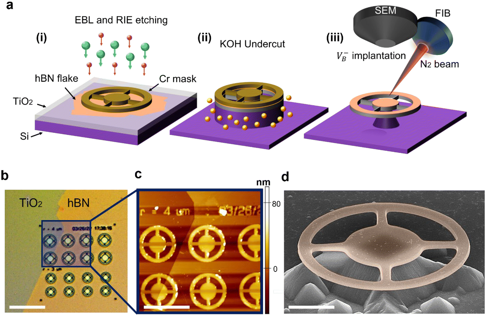 | ||
| Fig. 1 Fabrication of hBN/TiO2 hybrid resonator. (a) Schematic representation of the fabrication process: (i) lithography step to pattern a Cr metal mask (brown steering-wheels) on hBN/TiO2 heterostructure and then transferring the mask into the heterostructure using ICP/RIE. Green and pink balls represent SF6, and Hydrogen species used in the latter step, respectively. (ii) Undercut of hBN/TiO2 hybrid resonator using 10% KOH aqueous solution. (iii) Generation of spin defects in hBN using angled Nitrogen focused ion beam (FIB). (b) Optical image of aligned EBL pattern on the hBN/TiO2 heterostructure. Scale bar: 25 μm. (c) AFM image of the patterned area. Scale bar: 10 μm. (d) 52° Tilted SEM image of the final hBN/TiO2 hybrid resonator. The false color shows the microring. Scale bar: 2 μm. | ||
Fig. 1b shows an optical microscope image of the patterned sample. The spatially precise lithography on the flake is directly visible by optical contrast showing boundaries between hBN flake and the TiO2 substrate. The energy-dispersive X-ray spectroscopy (EDS) analysis after fabrication of the device also indicates the presence of hBN flake on top of the post-fabricated TiO2 resonator (Fig. SI-3†). An Atomic Force Microscopy (AFM) image was scanned over the patterned area to confirm the thickness of patterned hBN as shown in Fig. 1c and Fig. SI-2b.† A detailed structure of the final hybrid resonator is shown in a high-resolution SEM image in Fig. 1d. Further SEM images of the resonators are presented in the ESI† indicating the quality of the resonator after fabrication (Fig. SI-4†).
Next, we characterized the coupling of VB− to the TiO2 resonator using a confocal photoluminescence setup (Method section). The photoluminescence spectrum collected from the center of the ring (denoted as “off-ring”) is shown in Fig. 2a (blue spectra) and a relatively broad emission spectrum of VB− spanning from 750 to 850 nm was observed. In contrast, when VB− was excited on the ring (denoted as “on-ring”, red spectra), superimposed peaks resulting from the coupling of VB− emission to WGM of the rings were observed. Since the WGMs of the resonator cover entire VB− emission range with short FSR of ∼7 nm, overall VB− signals were significantly enhanced compared to those of from uncoupled region. The coupled signals were collected from the scattering point (the bright spot indicated by red circle in the inset) where the photons partially outcoupled into the objective. Since light is well confined inside the cavity, the scattering points are necessary for the photon collection from top of the ring. The holding arms on the ring resonator can be used as scattering points to collect the modes from suspended rings. A pristine TiO2 ring resonator without hBN was also measured as a reference (Fig. SI-5†). Normalized electric field distribution of Transverse Electric (TE) and Transverse Magnetic (TM) modes intensity was calculated using FDTD simulation as shown in Fig. 2b and Fig. SI-6.† Electric field profile of the TE WGMs concentrated at the middle of the device whilst the TM field maxima confined at the top and bottom surface of the resonator as shown in the cross-sectional views. The analysis of the individual peak from high resolution spectra is shown in Fig. 2c. A quality factor (Q = λ/Δλ) of 2137 was obtained after fitting the peak with Lorentzian function. Characterization of more devices are shown in Fig. SI-7a† and a mean quality factor of 1800 was achieved in this study.
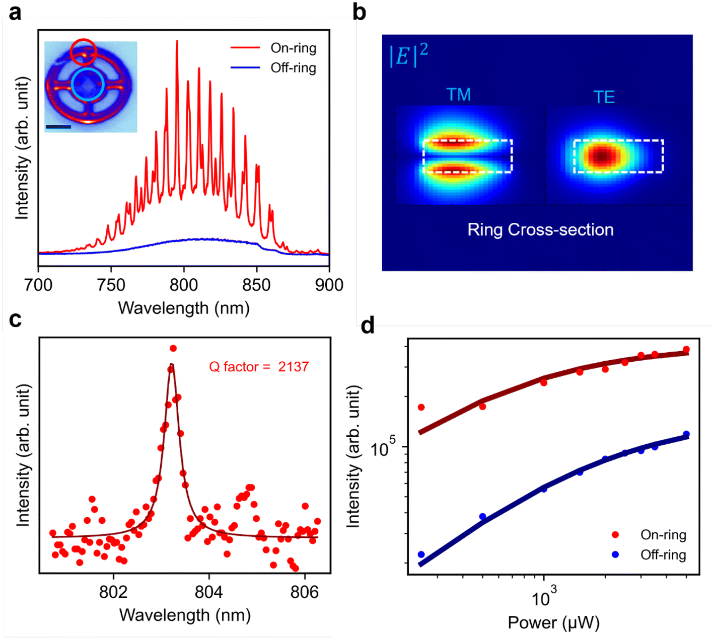 | ||
| Fig. 2 Optical characterization of the microring resonator. (a) PL spectrum collected on (red) and off (blue) the ring. Inset – confocal scanning image of the corresponding hybrid resonator. Red and blue circles indicate collection spots corresponding to On and Off the ring, respectively. Scale bar: 2 μm. (b) Cross-section view of the FDTD simulation for the fundamental TE (transverse electric) and TM (transverse magnetic) modes, showing electric field distribution of the fundamental modes inside the resonator. The dash box outlines the TiO2 cross-section view. (c) High-resolution spectra of the WGMs fitted by Lorentzian function yielding a quality factor of ∼2100 for the fabricated ring resonator (d) integrated PL intensity of the signals collected on (red) and off (blue) the ring at increasing excitation power. | ||
To further investigate the enhancement of the coupled signals, PL intensity was measured for both on-ring and off-ring emissions as a function of excitation power shown in Fig. 2d. The intensities for both cases, were integrated over the whole range of VB− emission, and the resulting data were fitted with the equation I = (IsatP)/(P + Psat), where Isat is the saturation intensity, and Psat is the saturation power. The saturation intensities of 0.405 MHz and 0.152 MHz and powers of 0.7 and 1.7 mW was obtained from the fit to the data (solid lines) for the on-ring and off-ring, respectively. These values yield the enhancement factor of about 3 and 7 in the saturated and unsaturated regimes.
In contrast, if each individual coupled signal is examined separately, the intensity of the coupled VB− emission is significantly higher than the uncoupled signal. For instance, we observed an enhancement factor of about 14 for the coupled signal at ∼790 nm as shown in Fig. SI-7b.†
Ultimately, to further characterize the hybrid devices, we employed ODMR spectroscopy to map spin transitions of the coupled VB− in local and non-local excitation configurations. The spin defect in hBN and its simplified electronic level structure is schematically depicted in Fig. 3a. The defect shows a triplet ground state (A13) with a zero-field splitting of 3.48 GHz between the two spin states. We evaluate spin transitions from VB− that coupled to WGM in the local and non-local configurations. In the local configuration, the optical collection and excitation spots were overlapped, while at the non-local configuration, the excitation of the microscope was offset 180° on the ring away from the collection spot. The results and the schematic configuration of both scenarios are shown in Fig. 3b. The spectra recorded from non-local configuration is shown in Fig. 3b (purple) with similar features as the local excitation (green) indicating the efficient coupling of VB− into the TiO2 ring resonator. We note that VB− can be excited by the guided laser in the ring as well. However, when the laser spot is fixed, no obvious emission on other part of the ring is detected, which highly suggest a low excitation efficiency in this scenario. Fig. 3c shows the corresponding ODMR signals for both excitation schemes. By sweeping a microwave from 3.2 to 3.8 GHz, a reduction in the photoluminescence of the VB− was detected at 3.4 and 3.5 GHz. These contrasts are the result of transitions from ms = 0 to ms = ±1 in the ground state which are driven by the microwave field (Fig. 3a). This verifies that VB− emits photons carrying spin information into the resonator and effectively coupled to the WGMs. The presence of spin transitions will confirm the boron vacancy defects are active in the hBN layer after fabrications. This is important for application of such structure utilizing spin properties of optically active spin defects in hBN. Both excitation scheme showed similar ODMR contrast with slight differences stemming from lower collection efficiency through non-local excitation.
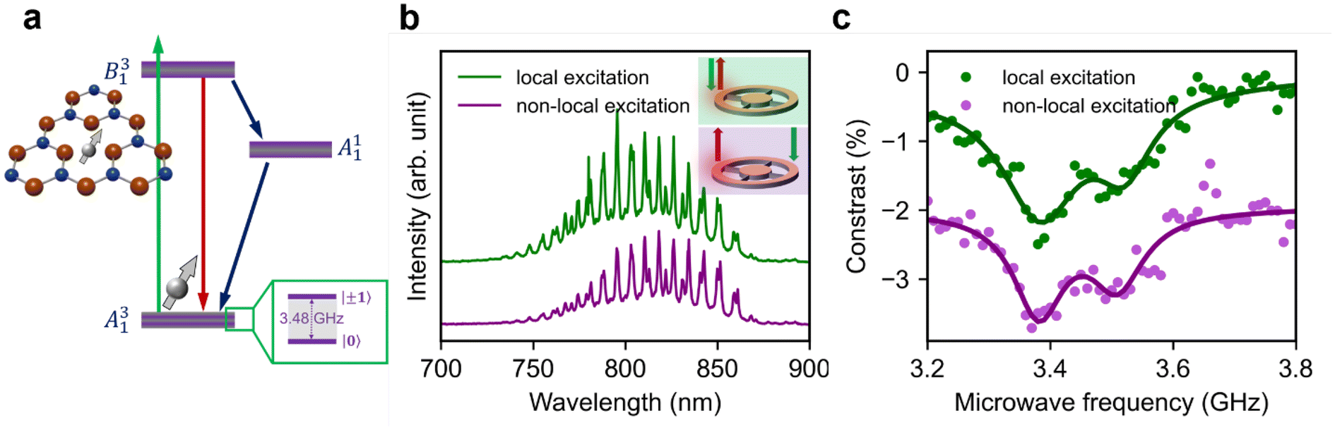 | ||
| Fig. 3 ODMR measurement of coupled VB−. (a) Schematic of the VB− defect and an energy diagram showing the main optical pumping cycle and the alternate cycle through the metastable state. (b) PL spectrum from coupled VB− in local and non-local configurations. The spectra were offset in Y-axis for clarity. The inset schematically shows these configurations. (c) ODMR measurement from coupled VB− in local and non-local configurations. The microwave power was set to 10 dB for both configurations. The ODMR contrast of the non-local excitation scheme was offset for clarity. | ||
In summary, we have developed a method for fabrication of a hBN/TiO2 resonators with high Quality factors exceeding ∼2000. Coupling of VB− to the WGM results in the increase of photoluminescence of about 7 and 3 in the unsaturated and saturated regimes, respectively. Finally, we demonstrated the coupling of VB−via two excitation configurations. Importantly, in a non-local configuration, the PL intensity and the ODMR signal collected from guided photons, indicating efficient coupling of VB− to TiO2 ring resonators. Our results are promising for scaling up integration of layered materials with nanophotonic resonators.
Methods
Hybrid resonator fabrication
Following the hBN transfer step, a thin layer of e-beam polymer resist (CSAR, AllResist GmBH) was spin-coated onto the sample for 60 s at 5000 rpm followed by baking on a hotplate at 170 °C for 2 minutes. EBL patterning was performed in SEM (Zeiss Supra 55 VP) with electron energy of 30 keV, 20 pA current and a base dose of 100 μC cm−2. The scanning beam was controlled by the Raith EBL system. After the development step, 50 nm Cr is deposited on the substrate using a magnetron sputtering machine. Afterwards, the residual polymer was removed in hot CSAR remover (AR600-71, AllResist GmBH). The patterns were transferred into the underlying hBN/TiO2/Si sample using ICP/RIE technique. A mixture of SF6/H2 as reactive gases were introduced into the ICP/RIE chamber with a ratio of 1:7 and then plasma was generated by RF power of 100 W. In the following step, the sample was immersed into a 10% KOH aqueous solution for continually 5 minutes and then placed into a beaker of water to stop basic reactions. After the undercut step, the Cr metal mask was stripped away using Cr etchant. The sample was then rinsed with IPA and water followed by annealing at 300 °C to clean the etchant and increase adhesion.
Ion implantation
The creation of boron vacancy defects is achieved by focused ion beam irradiation in a Helios G4 PFIB UXe DualBeam microscope. Ion irradiation is performed at 60° incidence angle with respect to the surface normal to maximize the number of defects in a thin flake. A N2 source is used, the beam energy and current are 5 kV and 75 pA respectively. A square irradiation pattern is defined over the resonator structure containing the hBN flake. The irradiation area and time are set to achieve an ion fluence of 1 × 1014.FDTD simulations
The FDTD was used to calculate the WGMs of a TiO2 ring resonator using commercial software (Lumerical FDTD). The TiO2 ring resonator with four arms clamping on the central disk was embedded in vacuum. All dimension parameters of the whole structure and the refractive index of TiO2 were taken from the experiment. TE/TM WGMs are excited with an in-plane electric/magnetic dipole lying on the ring avoiding the clamping points, respectively. The dipole orientation was perpendicular to the curvature of the ring. Perfectly Matched Layers (PML) were applied in all three directions. A time monitor was used to capture the decay of the field and convert the spectrum in frequency domain. The cut off wavelength of TM modes was around 1050 nm which was mainly controlled by the thickness of the ring resonator.PL characterization
PL spectra were recorded using a lab-built confocal setup. The devices were excited with a 532 nm continuous wave laser collimated and directed using several mirrors and lenses. The laser was focused onto the sample by a 100× and 0.9 NA objective forming around 500 nm spot through a 4f scanning system. The laser was scanned over the sample by a scanning mirror and the signals were collected by the same objective and transmitted back to the detectors. The signals were filtered by a 568 nm long pass filter and sent to a spectrometer (Princeton Instruments) or an avalanche photodiode APD (Excelitas) by a flip mirror.ODMR characterization
For the ODMR characterization, the samples were connected to a chip holder and a wire antenna (∼30 μm diameter) was placed next to the structures within a few tens of micrometers. To generate microwave signals, the current was passed through the antenna by a RF generator (AnaPico APSIN) and amplified (minicircuits, ZHL-16W-43-S+). Microwave was swept over 3.2 to 3.8 GHz at −10 dbm and PL signals were collected for 10 ms while the microwave field was on and off. The spin transitions were obtained by fitting a Lorentzian function to the data which yield two resonance frequencies at ∼3.4 and ∼3.5 GHz. The ODMR contrast was measured from the difference between the recorded signals in each frequency value.Conflicts of interest
There are no conflicts to declare.Acknowledgements
The authors acknowledge financial support from the Australian Research Council (CE200100010) for financial support, the Asian Office of Aerospace Research and Development (FA2386-20-1-4014) and the Office of Naval Research Global (N62909-22-1-2028). S.T.H acknowledges the support from AME Young Individual Research Grant (A2084c0177) and A*STAR MTC-Programmatic Fund (M21J9b0085)”. The authors thank the ANFF (UTS node) for use of the nanofabrication facilities.References
- J. D. Caldwell, I. Aharonovich, G. Cassabois, J. H. Edgar, B. Gil and D. N. Basov, Photonics with hexagonal boron nitride, Nat. Rev. Mater., 2019, 4, 552–567 CrossRef CAS.
- B. Gil, G. Cassabois, R. Cusco, G. Fugallo and L. Artus, Boron nitride for excitonics, nano photonics, and quantum technologies, Nanophotonics, 2020, 9, 3483–3504 CrossRef CAS.
- M. Kianinia, Z.-Q. Xu, M. Toth and I. Aharonovich, Quantum emitters in 2D materials: Emitter engineering, photophysics, and integration in photonic nanostructures, Appl. Phys. Rev., 2022, 9, 011306 CAS.
- J. Comtet, B. Grosjean, E. Glushkov, A. Avsar, K. Watanabe, T. Taniguchi, R. Vuilleumier, M.-L. Bocquet and A. Radenovic, Direct observation of water-mediated single-proton transport between hBN surface defects, Nat. Nanotech., 2020, 15, 598–604 CrossRef CAS PubMed.
- C. Fournier, A. Plaud, S. Roux, A. Pierret, M. Rosticher, K. Watanabe, T. Taniguchi, S. Buil, X. Quélin, J. Barjon, J.-P. Hermier and A. Delteil, Position-controlled quantum emitters with reproducible emission wavelength in hexagonal boron nitride, Nat. Commun., 2021, 12, 3779 CrossRef CAS PubMed.
- M. Atatüre, D. Englund, N. Vamivakas, S.-Y. Lee and J. Wrachtrup, Material platforms for spin-based photonic quantum technologies, Nat. Rev. Mater., 2018, 3, 38–51 CrossRef.
- D. D. Awschalom, R. Hanson, J. Wrachtrup and B. B. Zhou, Quantum technologies with optically interfaced solid-state spins, Nat. Photonics, 2018, 12, 516–527 CrossRef CAS.
- H. L. Stern, Q. Gu, J. Jarman, S. Eizagirre Barker, N. Mendelson, D. Chugh, S. Schott, H. H. Tan, H. Sirringhaus, I. Aharonovich and M. Atature, Room-temperature optically detected magnetic resonance of single defects in hexagonal boron nitride, Nat. Commun., 2022, 13, 618 CrossRef CAS PubMed.
- N. Mendelson, D. Chugh, J. R. Reimers, T. S. Cheng, A. Gottscholl, H. Long, C. J. Mellor, A. Zettl, V. Dyakonov and P. H. Beton, Identifying carbon as the source of visible single-photon emission from hexagonal boron nitride, Nat. Mater., 2021, 20, 321–328 CrossRef CAS PubMed.
- N. Chejanovsky, A. Mukherjee, J. Geng, Y. C. Chen, Y. Kim, A. Denisenko, A. Finkler, T. Taniguchi, K. Watanabe, D. B. R. Dasari, P. Auburger, A. Gali, J. H. Smet and J. Wrachtrup, Single-spin resonance in a van der Waals embedded paramagnetic defect, Nat. Mater., 2021, 20, 1079–1084 CrossRef CAS PubMed.
- A. Gottscholl, M. Kianinia, V. Soltamov, S. Orlinskii, G. Mamin, C. Bradac, C. Kasper, K. Krambrock, A. Sperlich, M. Toth, I. Aharonovich and V. Dyakonov, Initialization and read-out of intrinsic spin defects in a van der Waals crystal at room temperature, Nat. Mater., 2020, 19, 540–545 CrossRef CAS PubMed.
- X. Gao, B. Jiang, A. E. Llacsahuanga Allcca, K. Shen, M. A. Sadi, A. B. Solanki, P. Ju, Z. Xu, P. Upadhyaya, Y. P. Chen, S. A. Bhave and T. Li, High-Contrast Plasmonic-Enhanced Shallow Spin Defects in Hexagonal Boron Nitride for Quantum Sensing, Nano Lett., 2021, 21, 7708–7714 CrossRef CAS PubMed.
- N.-J. Guo, W. Liu, Z.-P. Li, Y.-Z. Yang, S. Yu, Y. Meng, Z.-A. Wang, X.-D. Zeng, F.-F. Yan, Q. Li, J.-F. Wang, J.-S. Xu, Y.-T. Wang, J.-S. Tang, C.-F. Li and G.-C. Guo, Generation of Spin Defects by Ion Implantation in Hexagonal Boron Nitride, ACS Omega, 2022, 7, 1733–1739 CrossRef CAS PubMed.
- M. Kianinia, S. White, J. E. Fröch, C. Bradac and I. Aharonovich, Generation of Spin Defects in Hexagonal Boron Nitride, ACS Photonics, 2020, 7, 2147–2152 CrossRef CAS.
- V. Ivády, G. Barcza, G. Thiering, S. Li, H. Hamdi, J.-P. Chou, Ö. Legeza and A. Gali, Ab initio theory of the negatively charged boron vacancy qubit in hexagonal boron nitride, npj Comput. Mater., 2020, 6, 41 CrossRef.
- A. Gottscholl, M. Diez, V. Soltamov, C. Kasper, A. Sperlich, M. Kianinia, C. Bradac, I. Aharonovich and V. Dyakonov, Room temperature coherent control of spin defects in hexagonal boron nitride, Sci. Adv., 2021, 7, eabf3630 CrossRef CAS PubMed.
- A. Gottscholl, M. Diez, V. Soltamov, C. Kasper, D. Krauße, A. Sperlich, M. Kianinia, C. Bradac, I. Aharonovich and V. Dyakonov, Spin defects in hBN as promising temperature, pressure and magnetic field quantum sensors, Nat. Commun., 2021, 12, 1–8 CrossRef PubMed.
- D. Curie, J. T. Krogel, L. Cavar, A. Solanki, P. Upadhyaya, T. Li, Y.-Y. Pai, M. Chilcote, V. Iyer and A. Puretzky, Correlative nanoscale imaging of strained hBN spin defects, arXiv preprint arXiv:2203.10075, 2022.
- P. Auburger and A. Gali, Towards ab initio identification of paramagnetic substitutional carbon defects in hexagonal boron nitride acting as quantum bits, Phys. Rev. B, 2021, 104, 075410 CrossRef CAS.
- T. Yang, N. Mendelson, C. Li, A. Gottscholl, J. Scott, M. Kianinia, V. Dyakonov, M. Toth and I. Aharonovich, Spin defects in hexagonal boron nitride for strain sensing on nanopillar arrays, Nanoscale, 2022, 14, 5239–5244 RSC.
- C. Qian, V. Villafañe, M. Schalk, G. V. Astakhov, U. Kentsch, M. Helm, P. Soubelet, N. P. Wilson, R. Rizzato and S. Mohr, Unveiling the Zero-Phonon Line of the Boron Vacancy Center by Cavity Enhanced Emission, arXiv preprint arXiv:2202.10980, 2022.
- S. Baber, R. N. E. Malein, P. Khatri, P. S. Keatley, S. Guo, F. Withers, A. J. Ramsay and I. J. Luxmoore, Excited State Spectroscopy of Boron Vacancy Defects in Hexagonal Boron Nitride Using Time-Resolved Optically Detected Magnetic Resonance, Nano Lett., 2022, 22, 461–467 CrossRef CAS PubMed.
- P. Yu, H. Sun, M. Wang, T. Zhang, X. Ye, J. Zhou, H. Liu, C.-J. Wang, F. Shi, Y. Wang and J. Du, Excited-State Spectroscopy of Spin Defects in Hexagonal Boron Nitride, Nano Lett., 2022, 3545 CrossRef CAS.
- N. Mathur, A. Mukherjee, X. Gao, J. Luo, B. A. Mccullian, T. Li, A. N. Vamivakas and G. D. Fuchs, Excited-state spin-resonance spectroscopy of VB defect centers in hexagonal boron nitride, https://arxiv.org/abs/2111.10855, 2021.
- J. E. Froch, L. P. Spencer, M. Kianinia, D. D. Totonjian, M. Nguyen, A. Gottscholl, V. Dyakonov, M. Toth, S. Kim and I. Aharonovich, Coupling Spin Defects in Hexagonal Boron Nitride to Monolithic Bullseye Cavities, Nano Lett., 2021, 21, 6549–6555 CrossRef CAS.
- N. Mendelson, R. Ritika, M. Kianinia, J. Scott, S. Kim, J. E. Froch, C. Gazzana, M. Westerhausen, L. Xiao, S. S. Mohajerani, S. Strauf, M. Toth, I. Aharonovich and Z. Q. Xu, Coupling Spin Defects in a Layered Material to Nanoscale Plasmonic Cavities, Adv. Mater., 2022, 34, e2106046 CrossRef PubMed.
- R. Khelifa, P. Back, N. Flory, S. Nashashibi, K. Malchow, T. Taniguchi, K. Watanabe, A. Jain and L. Novotny, Coupling Interlayer Excitons to Whispering Gallery Modes in van der Waals Heterostructures, Nano Lett., 2020, 20, 6155–6161 CrossRef CAS PubMed.
- Y. Ye, Z. J. Wong, X. Lu, X. Ni, H. Zhu, X. Chen, Y. Wang and X. Zhang, Monolayer excitonic laser, Nat. Photonics, 2015, 9, 733–737 CrossRef CAS.
- L. Wang, X. Zhou, S. Yang, G. Huang and Y. Mei, 2D-material-integrated whispering-gallery-mode microcavity, Photonics Res., 2019, 7, 905–916 CrossRef CAS.
- A. Das, D. J. Lee, P. K. Shandilya, S. Kim, G. Kang, D. P. Lake, B. Behera, D. Sukachev, I. Aharonovich and J.-H. Lee, Demonstration of hybrid high-Q hexagonal boron nitride microresonators, ACS Photonics, 2021, 8, 3027–3033 CrossRef CAS.
- A. Butcher, X. Guo, R. Shreiner, N. Delegan, K. Hao, P. J. Duda III, D. D. Awschalom, F. J. Heremans and A. A. High, High-Q nanophotonic resonators on diamond membranes using templated atomic layer deposition of TiO2, Nano Lett., 2020, 20, 4603–4609 CrossRef CAS PubMed.
- J. T. Choy, J. D. Bradley, P. B. Deotare, I. B. Burgess, C. C. Evans, E. Mazur and M. Lončar, Integrated TiO 2 resonators for visible photonics, Opt. Lett., 2012, 37, 539–541 CrossRef CAS PubMed.
- C. C. Evans, C. Liu and J. Suntivich, TiO2 nanophotonic sensors for efficient integrated evanescent Raman spectroscopy, ACS Photonics, 2016, 3, 1662–1669 CrossRef CAS.
- F. Qiu, A. M. Spring and S. Yokoyama, Athermal and high-Q hybrid TiO2–Si3N4 ring resonator via an etching-free fabrication technique, ACS Photonics, 2015, 2, 405–409 CrossRef CAS.
- N. V. Proscia, H. Jayakumar, X. Ge, G. Lopez-Morales, Z. Shotan, W. Zhou, C. A. Meriles and V. M. Menon, Microcavity-coupled emitters in hexagonal boron nitride, Nanophotonics, 2020, 9, 2937–2944 CrossRef CAS.
- J. D. Bradley, C. C. Evans, J. T. Choy, O. Reshef, P. B. Deotare, F. Parsy, K. C. Phillips, M. Lončar and E. Mazur, Submicrometer-wide amorphous and polycrystalline anatase TiO 2 waveguides for microphotonic devices, Opt. Express, 2012, 20, 23821–23831 CrossRef CAS PubMed.
Footnote |
| † Electronic supplementary information (ESI) available. See DOI: https://doi.org/10.1039/d2nr02522a |
| This journal is © The Royal Society of Chemistry 2022 |