
Materials nanoarchitectonics in a two-dimensional world within a nanoscale distance from the liquid phase
Katsuhiko
Ariga
 ab
ab
aWPI Research Center for Materials Nanoarchitectonics (MANA), National Institute for Materials Science (NIMS), 1-1 Namiki, Tsukuba, Ibaraki 305-0044, Japan
bGraduate School of Frontier Sciences, The University of Tokyo, 5-1-5 Kashiwanoha, Kashiwa, Chiba 277-8561, Japan
First published on 4th July 2022
Abstract
Promoted understanding of nanotechnology has enabled the construction of functional materials with nanoscale-regulated structures. Accordingly, materials science requires one-step further innovation by coupling nanotechnology with the other materials sciences. As a post-nanotechnology concept, nanoarchitectonics has recently been proposed. It is a methodology to architect functional material systems using atomic, molecular, and nanomaterial unit-components. One of the attractive methodologies would be to develop nanoarchitectonics in a defined dimensional environment with certain dynamism, such as liquid interfaces. However, nanoarchitectonics at liquid interfaces has not been fully explored because of difficulties in direct observations and evaluations with high-resolutions. This unsatisfied situation in the nanoscale understanding of liquid interfaces may keep liquid interfaces as unexplored and attractive frontiers in nanotechnology and nanoarchitectonics. Research efforts related to materials nanoarchitectonics on liquid interfaces have been continuously made. As exemplified in this review paper, a wide range of materials can be organized and functionalized on liquid interfaces, including organic molecules, inorganic nanomaterials, hybrids, organic semiconductor thin films, proteins, and stem cells. Two-dimensional nanocarbon sheets have been fabricated by molecular reactions at dynamically moving interfaces, and metal–organic frameworks and covalent organic frameworks have been fabricated by specific interactions and reactions at liquid interfaces. Therefore, functions such as sensors, devices, energy-related applications, and cell control are being explored. In fact, the potential for the nanoarchitectonics of functional materials in two-dimensional nanospaces at liquid surfaces is sufficiently high. On the basis of these backgrounds, this short review article describes recent approaches to materials nanoarchitectonics in a liquid-based two-dimensional world, i.e., interfacial regions within a nanoscale distance from the liquid phase.
 Katsuhiko Ariga | Katsuhiko Ariga received his Ph.D. degree from the Tokyo Institute of Technology in 1990. He joined the National Institute for Materials Science (NIMS) in 2004 and is currently the leader of the Supermolecules Group and principal investigator of the World Premier International (WPI) Research Centre for Materials Nanoarchitectonics (MANA), NIMS. He is also appointed as a professor at the University of Tokyo. |
1. Introduction
The synthesis of functional materials has encompassed many fields, including organic synthesis,1 inorganic chemistry,2 polymer chemistry,3 supramolecular chemistry,4 coordination chemistry,5 material chemistry,6 and biochemistry.7 It has become clear that not only the properties of the materials themselves, but also their internal structures and the component organization are important for the development of advanced functions. As a powerful methodology for high-resolution science and technology, nanotechnology has developed especially since the late 20th century. Nanotechnology enables us to observe structures and analyse phenomena at the atomic and molecular sizes (so called the nanoscale).8 Mainly based on developments of high-resolution microscopies9 and related analytical tools,10 one can consider the advocacy of the concept of nanotechnology to have stimulated research at the nanoscale. Promoted understanding of nanoscale materials has enabled the construction of functional materials with new insights. The progress of materials science with an emphasis on nanoscale properties has been considered in various research fields.11 However, these historical flows of materials science require one-step further innovation by coupling nanotechnology with the other materials fields. As a post-nanotechnology concept, nanoarchitectonics has recently been proposed (Fig. 1).12 It seeks to integrate nanotechnology with the fields of material production including organic, inorganic, and supramolecular chemistry, materials science, microfabrication technology, and bio-related technology.13 It is a methodology to architect functional material systems using atomic, molecular, and nanomaterial unit-components.14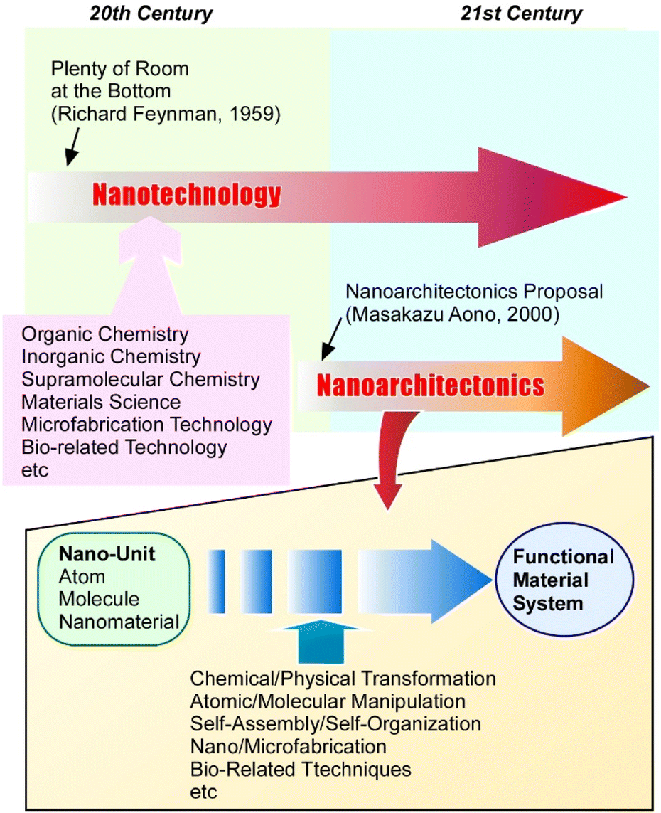 | ||
| Fig. 1 An outline of the nanoarchitectonics concept to integrate nanotechnology with the fields of material production including organic, inorganic, and supramolecular chemistry, materials science, microfabrication technology, and bio-related technology for the preparation of functional material systems using atomic, molecular, and nanomaterial unit-components. | ||
Just as Richard Feynman proposed nanotechnology,15 nanoarchitectonics was proposed by Masakazu Aono.16 In nanoarchitectonic approaches, various processes such as chemical/physical transformation, atomic/molecular manipulation, self-assembly/self-organization, nano/microfabrication, and bio-related techniques are selected and combined to architect functional material systems from nanoscale units.17 Because the methodology of nanoarchitectonics is so general, it can be applicable to a wide range of materials in various sizes. The latter feature also makes it possible to apply to a wide range of applications. For example, the nanoarchitectonics concept can be applied to material fabrication,18 structural control,19 catalysts,20 sensors,21 devices,22 energy-related23 and environmental24 applications, biochemical exploration,25 and biomedical applications.26 Considering that all materials are composed of atoms and molecules, this methodology of assembling materials from nano-units may be a method that can be applied to all materials. Like Theory of Everything in physics,27 nanoarchitectonics may be considered as a Method for Everything in materials science.28
Nanoarchitectonics is particularly suited for the fabrication of hierarchical structures because it combines processes that include not only the self-assembly of components but also human manipulation, such as the Langmuir–Blodgett (LB) method,29 layer-by-layer (LbL) assembly,30 and various microfabrication methods.31 The high capability of nanoarchitectonics for the fabrication of hierarchical functional structures32 shares features of structural constructions seen in biological systems in which huge numbers of functional components are hierarchically organized and their functions are linked together.33 The working principles of nanoarchitectonics organization also resemble those of biological systems. Material interactions at the nanoscale for nanoarchitectonics are often subject to perturbations such as thermal fluctuations, stochastic distributions, and quantum effects. Thus, in nanoarchitectonics, assembling functional structures from the nanoscale is a matter of harmonizing several effects rather than a simple summation of contributing effects.34 This characteristic is similar to that of biological systems, where many functional molecules work in tandem in the presence of thermal fluctuations to architect a functional system. Therefore, the ultimate goal of nanoarchitectonics is to create a functional material system in which a number of functions work flexibly together in a hierarchical structure like biological systems.35
In realistic fact, it is difficult to organize such a hierarchical functional system in freely expanded three-dimensional media. In biological systems, various proteins and pigments are often organized in the two-dimensionally confined space of cell membranes where high functions such as energy harvesting/conversion and signal transduction are performed.36 From this viewpoint, it is an attractive methodology to develop functional structures through nanoarchitectonics in defined and dimensionally confined environments. One of the attractive environments is a solid surface. Various nanoarchitectonic events including chemical conversions37 and materials/molecular organization38 have been researched for various functions such as sensing and bio-interactions. Nanoscale phenomena at solid interfaces can be often precisely observed and evaluated with nanotechnological tools.39 In contrast, nanoscale phenomena at liquid interfaces have not been fully explored because of certain difficulties in direct high-resolution observations. However, these unsatisfied situations in the nanoscale understanding of liquid interfaces may keep liquid interfaces as unexplored and attractive frontiers in nanotechnology and nanoarchitectonics.40
On the basis of these backgrounds, this short review article describes recent approaches to materials nanoarchitectonics in a liquid-based two-dimensional world i.e. interfacial regions within a nanoscale distance from the liquid phase (Fig. 2), by selecting several component materials including (i) organic molecules and materials, (ii) inorganic nanomaterials, (iii) metal–organic frameworks (MOFs) and covalent organic frameworks (COFs), (iv) organic semiconductors, and (v) proteins and stem cells. Selected examples cannot cover all the features of the related research fields, but they can tell typical features of molecular nanoarchitectonics at liquid interfaces and their high potential in applications.
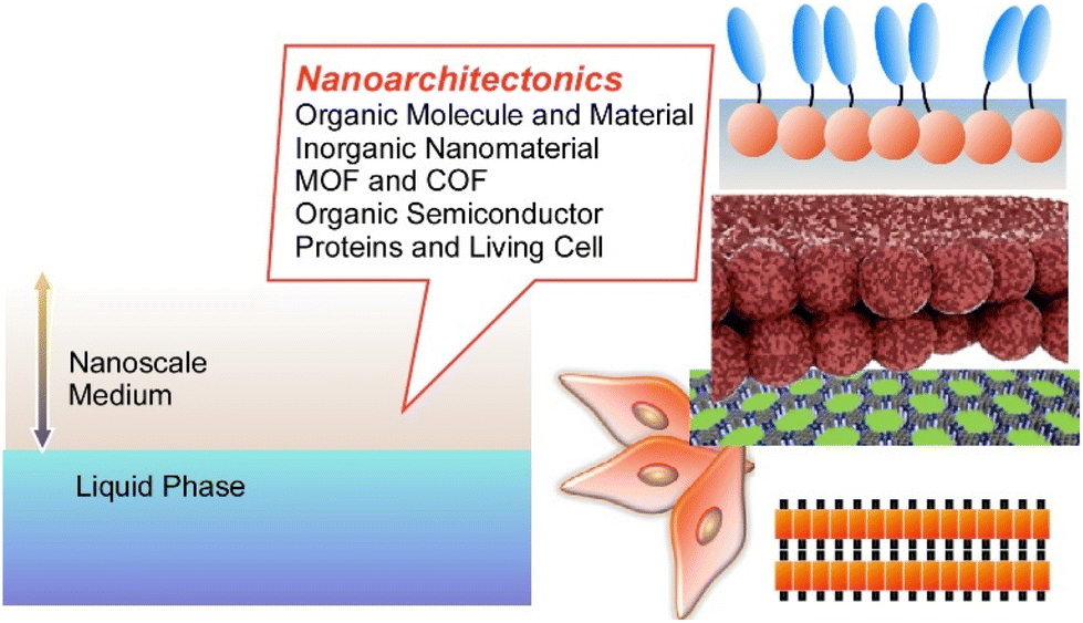 | ||
| Fig. 2 Subjects of this review article: materials nanoarchitectonics in a liquid-based two-dimensional world i.e. interfacial regions within a nanoscale distance from the liquid phase. | ||
2. Organic molecules and related materials
One of the representative methodologies to architect organized structures on liquid surfaces would be the Langmuir–Blodgett (LB) technique.41 The LB method is basically applied to lipids, surfactants, and amphiphiles to form uniform nanofilm architectures. However, its applicability is not limited to these typical film components. Thin film organizations were actually demonstrated for various nanomaterials,42 two-dimensional materials,43 and biomaterials such as proteins44 using the LB technique. Furthermore, forefront objects such as supramolecular polymers,45 DNA origami pieces,46 molecular machines,47 and artificial receptors48 can be subjected to the LB technique. The LB method is basically conducted at the air–water interfaces where water-soluble and water-insoluble substances can be encountered within two-dimensional spaces with a nanometer-level thickness. Molecular interactions are often enhanced at the air–water interface as compared with bulk water media.49 The latter feature is effectively working in highly sensitive molecular recognitions, further leading to the formation of specific two-dimensional patterns even with subnanometer-level structural precisions.50 Although the LB method is a 100-year-old traditional technique, it still has potential in materials nanoarchitectonics on liquid phases.51Accordingly, molecular arrangements and materials organizations at the air–water interface have been continuously explored. As exemplified below, various organic substances are used as active components in thin film nanoarchitectonics on water using the LB technique. Makiura et al. investigated surface-pressure-dependent self-assembling behaviours of liquid crystalline molecules conjugated with bio-components of peptides (Arg–Gly–Asp and Gly–Gly–Asp) (Fig. 3).52 Molecular orientation is an important key to determine the ordering of liquid crystalline nanoarchitectures at interfaces. Two-dimensional nanoarchitectonics with bioconjugated mesogens leads to the arrangement regulation of bio-recognizable molecular units at surfaces for developing biosensing devices. Delicate processes within two-dimensionally confined spaces sometimes lead to materials nanoarchitectonics with high structural precisions. Oishi and co-workers recently reported the formation of two-dimensional maze patterns with meandering domain patterns with a width of only nanometer orders through simple mixing of two kinds of fatty acids, palmitic acid and behenic acid, at the air–water interface (Fig. 4).53 These structurally precise patterns are probably nanoarchitected through fixation of a two-dimensional morphology on the way to phase separation. Such delicate patterns would be useful in certain kinds of advanced applications such as nanoelectronics, nanophotonics, and nanosensing.
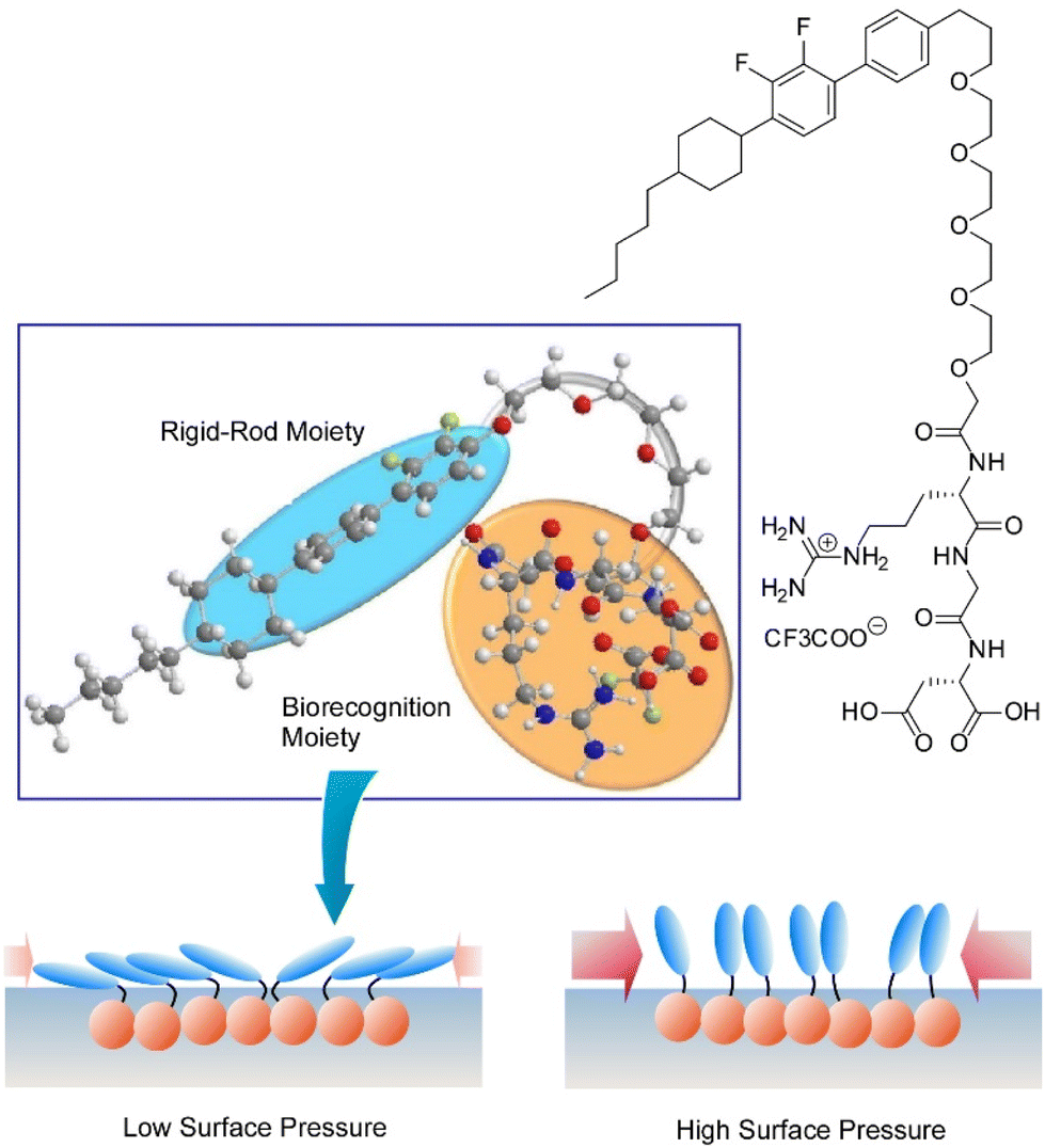 | ||
| Fig. 3 Surface-pressure-dependent self-assembling behaviours of liquid crystalline molecules conjugated with bio-components of peptides. Reproduced with permission from ref. 52. Copyright 2021 Chemical Society of Japan. | ||
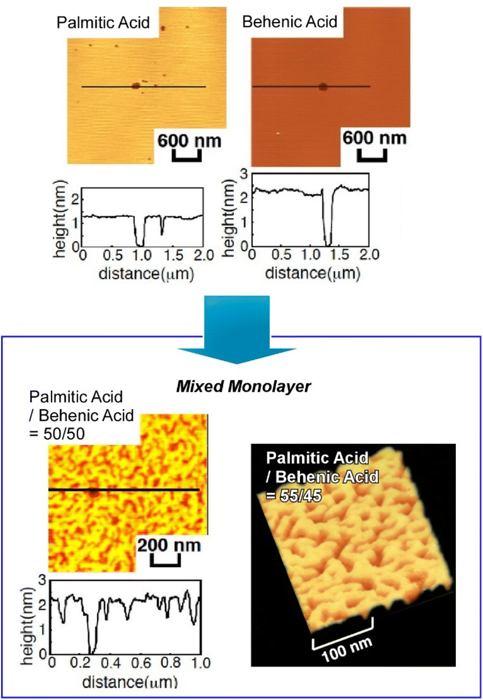 | ||
| Fig. 4 Formation of two-dimensional maze patterns with meandering domain patterns through simple mixing of two kinds of fatty acids, palmitic acid and behenic acid, at the air–water interface. Reproduced with permission from ref. 53. Copyright 2021 Chemical Society of Japan. | ||
Soft materials are also subjected to morphological studies at liquid interfaces. Yamagishi et al. investigated the effects of alkyl chain lengths and optical purities of interfacial behaviours of chiral perfluorinated gelators, N,N′-diperfluoroalkanoyl-1,2(R,R)-diaminocyclohexanes.54 Analyses of the transferred films by atomic force microscopy (AFM) and p-polarized infrared multiple angle incidence resolution spectrometry (pMAIRS)55 revealed structural transformation upon compression depending on optical purity. Camerin et al. applied theoretical modelling to investigate microgel behaviours at a flat water–oil interface (Fig. 5).56 Through the inclusion of realistic characteristics in internal polymeric structures and single particle properties of the target microgels, microgel shapes experimentally observed at the water–oil interface can be successfully reproduced. The obtained knowledge would give intuitions for microgel behaviours at surface media such as stabilization of smart emulsions and versatile surface patterning, which are also useful for biomedicine for noninvasive control over cell-adhesion.
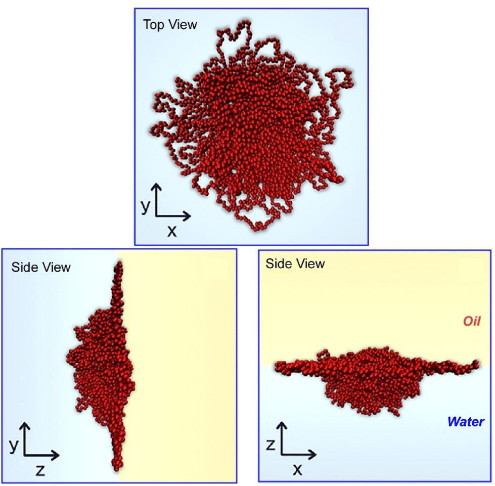 | ||
| Fig. 5 Theoretical modelling on microgel behaviours at a flat water–oil interface. Reproduced from ref. 56, under the terms of the CC BY. | ||
It is common knowledge that the LB method is performed on a clean water surface and under conditions that minimize vibration and other perturbations. In contrast, the vortex LB method was developed to create an organized structure on the liquid surface by inducing dynamic flows in the subphase.57 In the vortex LB method, nanomaterials on the liquid surface spontaneously assemble and form organized structures upon rotating the subphase. Mori et al. applied the vortex LB method to molecules and reported the fabrication of two-dimensional nanocarbon thin films with a nanometer level thickness (Fig. 6).58 Two-dimensional carbon materials (carbon nanosheets), such as graphene-related materials, are attracting attention as powerful electronic, optical, and catalytic materials. Preparation of two-dimensional materials sometimes requires expensive equipment and advanced technology. Therefore, like the vortex LB technique, a method to obtain two-dimensional carbon nanosheets using simple procedures and inexpensive apparatus is desired. In the reported method, a new carbon-rich π-conjugated anisotropic macrocycle, 9,9′,10,10′-tetra-butoxy-cyclo[6]-paraphenylene-[2]-3,6-phenanthrenylene (carbon nanoring molecule), was used as a carbon source. The ellipsoidal carbon nanoring molecules effectively afforded smooth two-dimensional molecular films through self-assembly at a dynamic liquid interface with a vortex motion. The thin films of carbon nanoring molecule assembly can be transferred onto a solid surface.
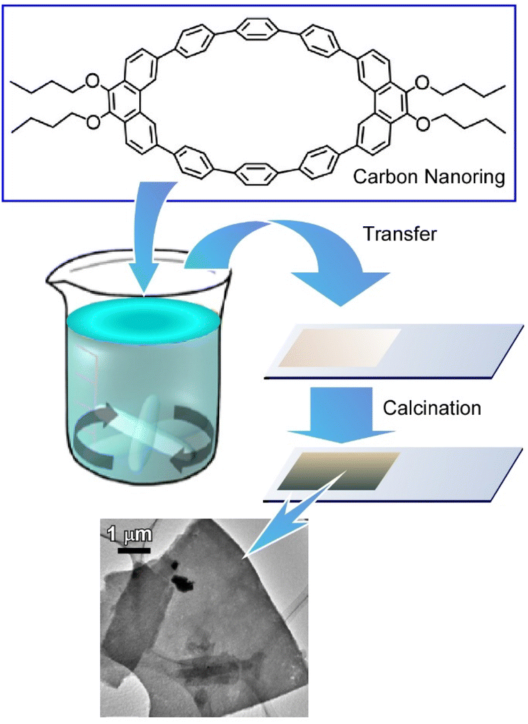 | ||
| Fig. 6 Fabrication of two-dimensional nanocarbon thin films with a nanometer level thickness by the vortex LB method and calcination. | ||
The fabricated thin films were then subjected to a carbonization process, resulting in carbon nanosheets. The two-dimensional morphology was retained even after the high-temperature carbonization process accompanied by a significant increase of electrical conductivity. In addition, nitrogen-doping for the carbon nanosheets can be done simply through the addition of pyridine as a nitrogen dopant to carbon nanoring molecules and the subsequent carbonization. The vortex LB method can be applied to molecules and materials for which it has been difficult to fabricate uniform thin films in the conventional LB method. Because this method requires only a beaker and a stirrer, it is expected to be widely used. Furthermore, the amount of carbon nanorings required to fabricate a 1 meter square nanosheet is extremely small, at only 1 nanogram. This technique can be industrially developed to produce large-scale carbon nanosheets due to its simplicity and inexpensive nature. Nitrogen-doped carbon nanosheets might be expected to be applied to fuel cells as a catalyst that can replace the expensive platinum.
As seen in the above-mentioned example, the ability to prepare tailored nanostructures is a critical aspect of the development of functional materials for different applications. Fullerene-based nanomaterials have been widely used to fabricate electronic devices, energy and light harvesting materials, biomaterials, etc.,59 and there exists important motivation to prepare various self-assembled fullerene nanostructures for the exploitation of their properties in functional systems.60 Fullerene can be assembled into higher dimensional morphologies including one-dimensional nanorods and nanotubes,61 two-dimensional nanosheets and nanodisks,62 and three-dimensional nanocubes63 upon precipitation at liquid–liquid interfaces. Among them, the nanoarchitectonics of ultrathin two-dimensional nanoporous materials with high applicability such as enhanced contrast sensitivity and spatial resolution in sensing is an attractive target. Recently Song et al. demonstrated the preparation of a novel two-dimensional ultrathin carbon material with hierarchical surfaces containing microporous and mesoporous structures by the reaction/assembly of fullerene and ethylenediamine molecules followed by thermal annealing of the resulting thin film (Fig. 7).64 The new film materials, coined by the term ‘fullerphenes’, exhibit supersensitive performance in the detection of formic acid. In the first process, a monolayer of fullerene C60–ethylenediamine was prepared at the microscopic liquid–liquid interface between m-xylene and water using the Pickering emulsion method. Observation by transmission electron microscopy (TEM) confirmed a large area homogeneous ultrathin film morphology. The fabricated C60–ethylenediamine films were then transformed directly into fullerphene films through thermal annealing at 700 °C under a nitrogen gas atmosphere. After the carbonization process, the fullerphenes remained as amorphous carbon films made from nanometer-sized, randomly oriented networks with a thickness of ca. 2 nm.
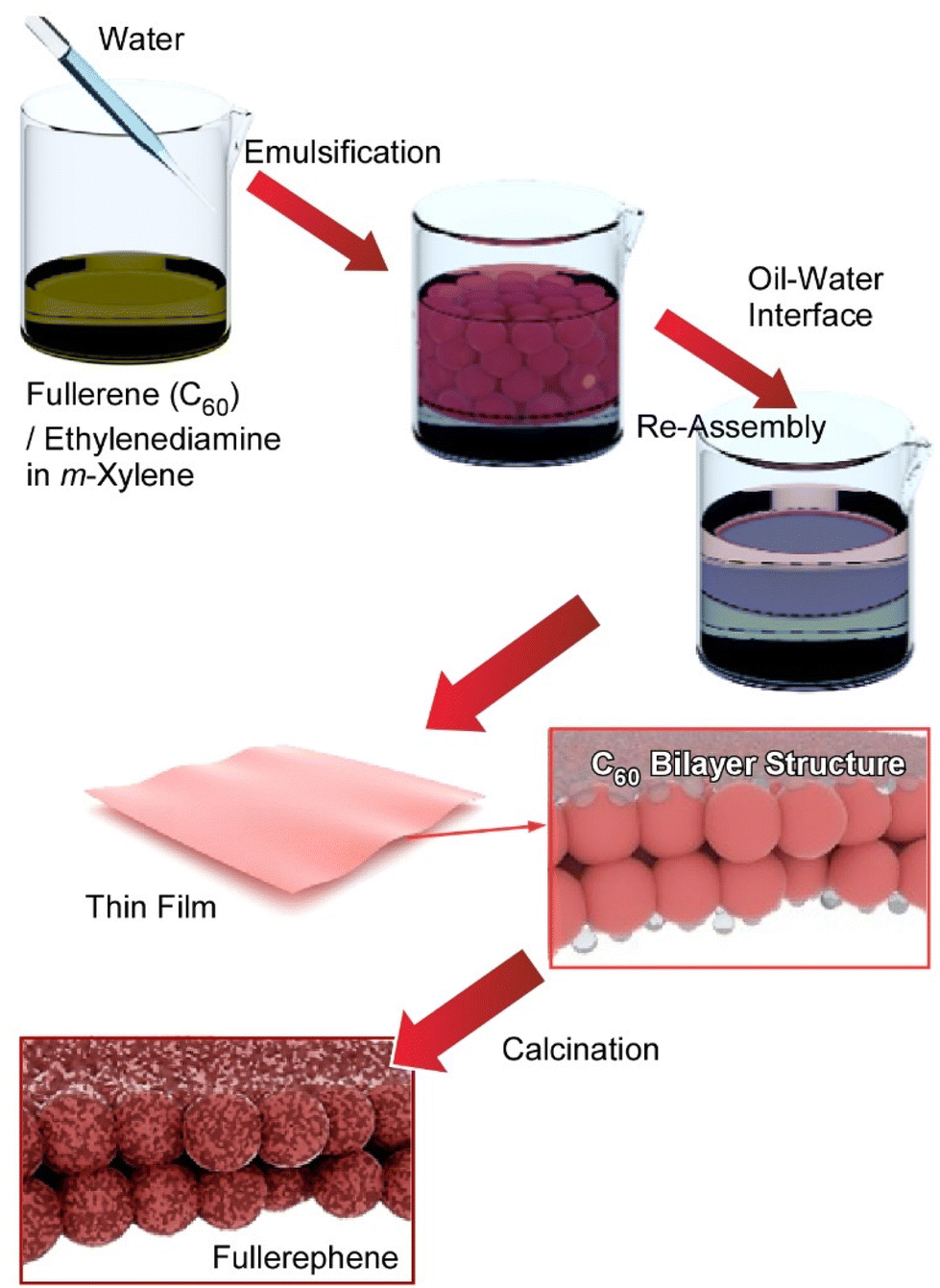 | ||
| Fig. 7 Preparation of a two-dimensional ultrathin carbon material with hierarchical surfaces containing microporous and mesoporous structures (fullerphene) by the reaction/assembly of fullerene and ethylenediamine molecules followed by thermal annealing of the resulting thin film. | ||
Fullerphene films were immobilized on a quartz crystal microbalance (QCM) and developed as a selective sensing device for volatile organic compound (VOC) detection. Among the 15 VOCs tested, the sensor showed the highest sensitivity to formic acid, and the sensing response showed excellent reproducibility for repeated use. The OCM sensor was basically shown to have excellent sensitivity to acid VOCs due to the presence of basic groups. The response to formic acid is about 19 times greater than that to acetic acid and 163 times greater than that to water. These results indicate that the adsorption of acids from the gas phase onto the fullerene-modified QCM sensor depends not only on the acidity but also on the molecular dimensions of the acid to be analysed. Hierarchically micro- and mesoporous structures in fullerphene films, having a half pore width of ca. 0.27 nm and a mesopore diameter of ca. 3.67 nm, offer highly efficient transport pathways for the diffusion of formic acid whose largest molecular dimension is 0.28 nm. This is thought to be due to the nanoporous structure of the fullerphene films, which allows molecular discrimination at the level of a single carbon atom. Because the fullerphene is obtained by the bottom-up self-assembly of the fullerene molecule, no exfoliation process is required. Furthermore, fullerphene has an ultrafine porous nanostructure composed mainly of sp2-bonded carbon atoms and doped with nitrogen atoms dominated by pyrrole nitrogen and quaternary nitrogen. This structure also has potential for various applications other than sensing.
This section is summarized as follows. Liquid surfaces, such as the air–water interface, are ideal venues for two-dimensional nanoarchitectonics of organic molecules. Many examples have been investigated using traditional LB methods. The applied organic molecules are not limited to typical amphiphilic compounds, but can be applied to many water insoluble materials. The expansion of applicable materials also applies to many inorganic nanomaterials, as shown in the next section. As shown in the last two examples in this section, the liquid interfaces are also useful as media for nanomaterial synthesis. By imparting flow to the liquid interface, assembling carbon nanoring molecules in two-dimensions, and then processing them at high temperatures on a substrate, carbon nanosheets with nanometer-scale thickness and large lateral areas can be synthesized. The advantage of this two-dimensional bottom-up method is also found in the fact that heteroatom doping can easily be achieved by mixing additives. This simple procedure resulted in drastic changes in the electrical properties of the nanofilm. In addition, large-area nanofilms (fullerphene) can also be synthesized from fullerene molecules using emulsions with integrated liquid–liquid interfaces. The fullerphene films have a nanometer-scale thickness with finely tuned pores as characteristics of bottom-up processes. Such a delicate structure leads to fine molecular discrimination in their sensor usages. Nanoarchitectonics at the liquid interface can be a powerful method for the fabrication of highly functional nanofilms from organic molecules.
3. Inorganic nanomaterials
Thin films of inorganic materials are often synthesized using tedious processes and/or expensive instrumentation. From application viewpoints, inexpensive and simple processes to produce inorganic thin films have been explored. Recently, Malgras, Yamauchi, and co-workers reported the fabrication of thin films of inorganic hybrids by chemical reactions and spontaneous exfoliation processes on solid surfaces.65 Hybrid thin films consisting of amorphous titania embedded in ordered block copolymer micelles generated on solid surfaces can be exfoliated by alkali treatment. It is also important to neutralize the solution to prevent re-dissolution of the titania species. This is an effective method for transferring and immobilizing mesoporous titania films to a variety of substrates. Like this example, it is important to use bottom-up chemistry to fabricate inorganic thin film structures. Similarly, other methods have also been investigated for the preparation of organized thin films of inorganic materials on liquid surfaces. For example, the fabrication of organized inorganic thin films by the LB method is one promising method.Nanoarchitecting various nanowires into organized assemblies with optical, electrical, and multifunctional properties is a promising methodology for the next generation of multifunctional electronics. Liu, Yu, and co-workers co-assembled W18O49 and V2O5 nanowires by the LB method to demonstrate a new type of multicolor electrochromic device (Fig. 8).66 The transparent W18O49 nanowire film turned orange through increasing contents of V2O5 nanowires. In a three-electrode configuration with platinum wire as the counter electrode and Ag/AgCl as the reference electrode, the films exhibited pale orange, green, and gray colors upon application of voltages at 2, 0, and −0.5 V. In addition, different patterns can be easily fabricated by adding the corresponding masks. As shown in the figure, the chameleon pattern clearly showed orange, green, and gray colors when the corresponding bias voltage was applied. The proposed method is useful for assembling solid-state electrochromic devices, suggesting great potential for smart windows and multicolor electrochromic displays.
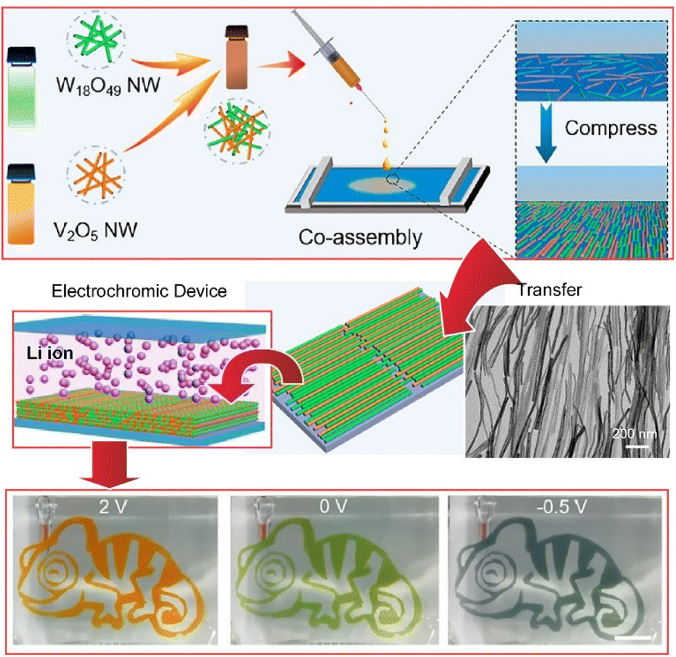 | ||
| Fig. 8 Co-assembled W18O49 and V2O5 nanowires by the LB method to demonstrate multicolor electrochromic devices that exhibited pale orange, green, and gray colors upon application of voltages at 2, 0, and −0.5 V. Reproduced with permission from ref. 66. Copyright 2021 American Chemical Society. | ||
It is well known that the amazing iridescent colors of insect shells reflect the complex nanoscale organization of biological fibers. Such materials have potential for a wide range of applications, including circularly polarized plates and lasers for circularly polarized light emission. Tang and co-workers have demonstrated the fabrication of Langmuir–Schaefer biomimetic chiral photonic crystals of colloidal inorganic nanowires.67 Not only did they reproduce the complex helical structure and circularly polarized color reflections observed in cord worms, they also achieved the highest asymmetric coefficient of chiroptical activity reported for chiral inorganic nanostructures. In addition, programmable structural control based on precise interlayer arrangements allows unprecedented freedom of manipulation of the optical activity of the fabricated chiral photonic crystals. It is envisioned that many inorganic nanomaterials with excellent optical, electrical, and magnetic properties can be incorporated into chiral photonic crystals by this method for the development of multifunctional devices.
Organized thin film structures of graphene oxide-based two-dimensional nanomaterials are expected to find applications in many fields.68 Therefore, a simple preparation method for such organized structures has attracted much attention. Jiao and co-workers reported the regulation of the aggregate state in graphene oxideporphyrin composite monolayers.69 In the initial step, diazotization and Fischer osazone reactions were used to prepare graphene oxide sheets in different surface states modified with sulfonic acid groups. The prepared amphiphilic surface-modified graphene oxide nanosheets spontaneously form composite films with porphyrin molecules (5,10,15,20-tetrakis(1-methyl-4-pyridinio)porphyrin, TMPyP) at the air–water interface through electrostatic interactions and π–π interactions. The TMPyP molecules can adsorb from the subphase onto graphene oxide into highly ordered J-aggregate structures. Morphological characterization indicated that the composite films had smooth and dense surfaces. The aggregation state of the porphyrin molecules was also different depending on the surface state of the nanosheets. It suggests that the introduction of sulfonic acid groups and the type of oxygen-containing group play an important role in controlling the aggregation state of porphyrin molecules.
Similarly, studies on the functionalization of two-dimensional materials such as black phosphorus are attractive targets from application viewpoints. Wang et al. fabricated composite films based on black phosphorus and dyes by the LB technique (Fig. 9).70 Black phosphorus nanosheets were first modified and stabilized with polyethyleneimine. The addition of polyethyleneimine reduces the contact between the black phosphorus nanosheets and oxygen, effectively improving the stability of the black phosphorus nanosheets. In combination with the LB technique, the solution of the complex was dispersed on the surface of the dye solution and transferred. The resulting composite LB film exhibited a color change against acidic and basic gases with good sensitivity. In addition, the composite films have surface-enhancing performance against crystal violet molecules. This research provides a new research avenue for the fabrication of multifunctional black phosphorus composite films and is expected to have a wide range of applications, including gas sensors and surface-enhanced Raman scattering.
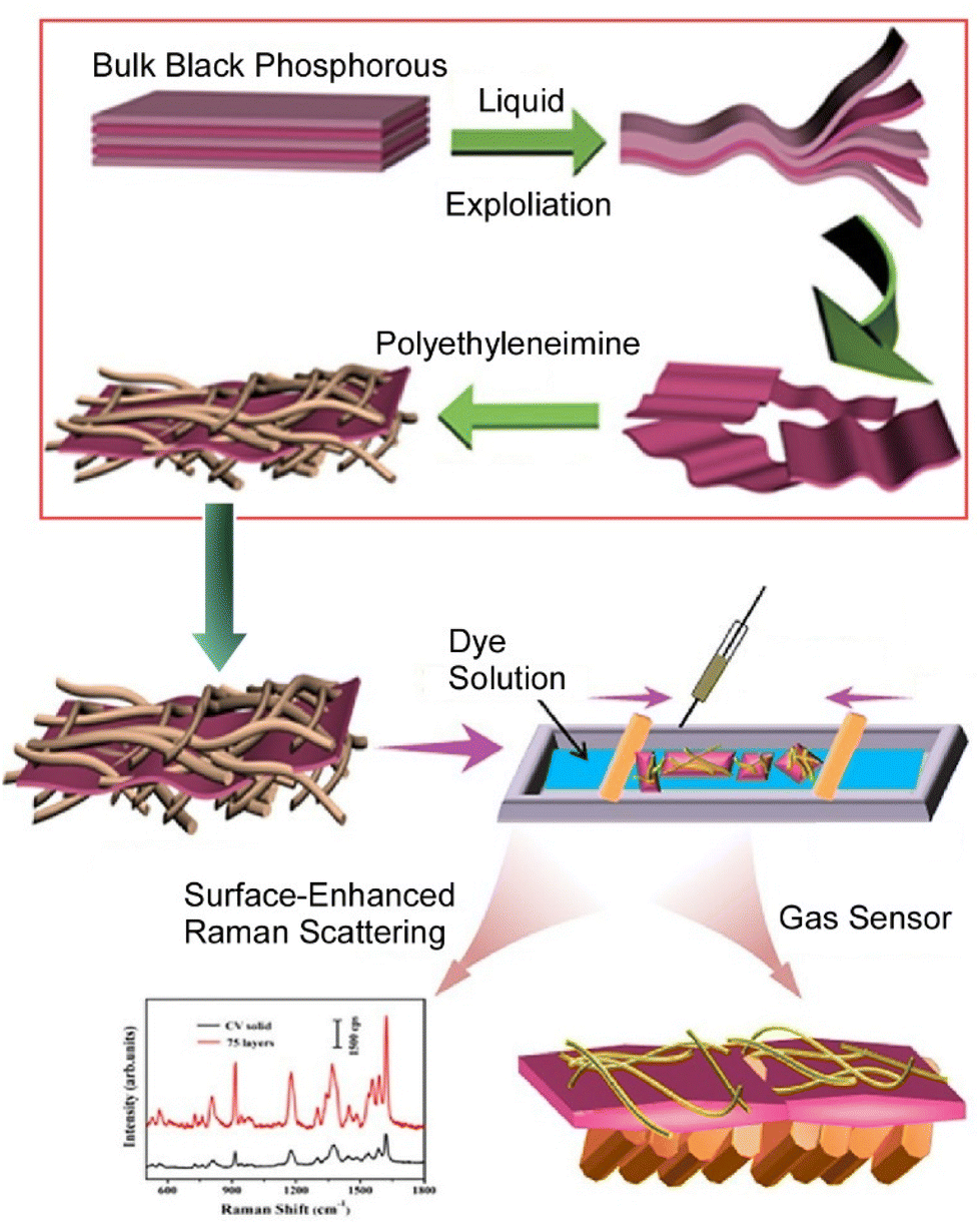 | ||
| Fig. 9 Fabrication of composite films based on black phosphorus and dyes by the LB technique for a wide range of applications including gas sensors and surface-enhanced Raman scattering. Reproduced with permission from ref. 70. Copyright 2020 American Chemical Society. | ||
A practical lithium metal battery must fully and reversibly utilize a thin metallic lithium anode. This raises the fundamental question of how to fabricate solid-electrolyte interphases that can control interfacial transport and protect reactive metals without increasing battery mass. Archer, Cho, and co-workers reported on the physicochemical properties of LB artificial solid-electrolyte interphases prepared using phosphate-functionalized reduced graphene oxide.71 LB artificial solid-electrolyte interphases not only meet the challenge of stabilizing Li anodes, but can also be easily assembled in a simple and scalable process. The LB artificial solid-electrolyte interphases can form durable coatings of Li that control electromigration at the anode–electrolyte interface. The stable operation of these batteries was reported as a first step toward the practical application of batteries with matched anode and cathode capacities in coin cells and pouch cells.
Zinc metal is a promising anode for aqueous zinc ion batteries due to its high volumetric capacity and low redox potential. However, dendrite growth significantly destabilizes the electrode/electrolyte interface, accelerating the occurrence of side reactions and ultimately degrading the electrochemical performance. Xie, Chen, and co-workers prepared thin films of nitrogen-doped graphene oxide as parallel and ultra-thin interface modified layers (about 120 nm) on a Zn foil (Fig. 10).72 The parallel graphene layer and the beneficial zinc affinity properties of the N-doped groups resulted in the directional deposition of Zn crystals on the (002) plane. On the other hand, in situ differential electrochemical mass spectrometry and in situ Raman measurements showed that the directional plating morphology of metallic Zn at the interface effectively suppresses hydrogen evolution reactions and passivation. As a result, a pouch-type battery combining this new anode with a LiMn2O4 cathode was able to maintain an extraordinary energy density at a moderate depth of discharge of 36%. This study provides an accessible synthesis method and detailed mechanistic analysis to accelerate the application of high energy density aqueous Zn-ion batteries. This facile method provides a new direction for the synthesis of ultrathin interfacial modifications that is expected to facilitate the large-scale application of Zn-based aqueous batteries.
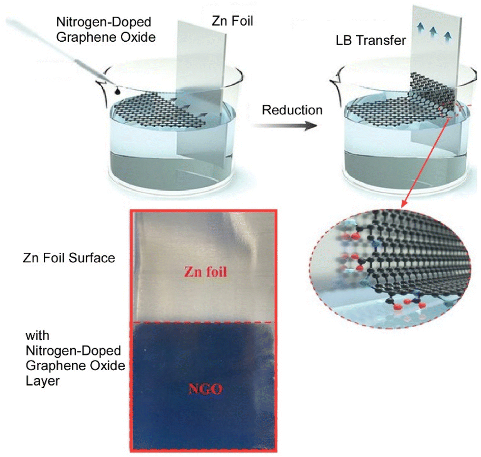 | ||
| Fig. 10 Preparation of thin films of nitrogen-doped graphene oxide as ultra-thin interface modified layers on a Zn foil through the LB method. Reproduced with permission from ref. 72. Copyright 2021 Wiley-VCH. | ||
Next-generation displays place stringent demands on resolution and color gamut as the number of pixels increases. Li, Qian, and co-workers have realized quantum dot light-emitting diodes with an ultra-high resolution of 9072 to 25![[thin space (1/6-em)]](https://www.rsc.org/images/entities/char_2009.gif) 400 pixels per inch using transfer printing and the LB film technology.73 A non-emissive charge barrier layer of wide bandgap quantum dots arranged in a honeycomb shape between the quantum dot pixels reduces leakage current. Red and green quantum dot light-emitting diodes were demonstrated. In particular, the red device achieved a maximum luminance of 262400 cd m−2 at an applied voltage of 8 V with a peak external quantum efficiency of 14.72%. This approach provides a promising means to realize ultra-high resolution and high performance quantum dot light-emitting diode devices. This new quantum dot patterning method opens new avenues for the realization of high performance, ultra-high-resolution quantum dot light-emitting diodes.
400 pixels per inch using transfer printing and the LB film technology.73 A non-emissive charge barrier layer of wide bandgap quantum dots arranged in a honeycomb shape between the quantum dot pixels reduces leakage current. Red and green quantum dot light-emitting diodes were demonstrated. In particular, the red device achieved a maximum luminance of 262400 cd m−2 at an applied voltage of 8 V with a peak external quantum efficiency of 14.72%. This approach provides a promising means to realize ultra-high resolution and high performance quantum dot light-emitting diode devices. This new quantum dot patterning method opens new avenues for the realization of high performance, ultra-high-resolution quantum dot light-emitting diodes.
A spiking neural network with artificial synapses and artificial neurons has the potential to achieve human-level intelligence. However, the fabrication of large-scale artificial neurons with good performance is still difficult due to the lack of suitable material systems and integration methods. Liu and co-workers reported the controllable integration of solution-treated two-dimensional single-walled titanium oxide nanosheets to produce ultra-thin, sub-10 nm size two-dimensional oxide-based artificial neuron systems (Fig. 11).74 The artificial neuron also consists of input, nerve body, and output. In this artificial neuron device, an ultrathin two-dimensional TiOx membrane is regarded as the neuronal membrane. The artificial neuron arrays are fabricated by controllable wet-coating LB assembly. The devices exhibit typical threshold resistance switching with volatile transitions and a high on/off ratio of 109, and can emulate leaky integrate-and-fire and self-healing without additional manipulation for sensing and resetting. It also offers long-term stability, fast switching, fast recovery, and low power consumption of 5 nJ. In the artificial neural array, each device shows stable switching behaviour, demonstrating the feasibility of this strategy in integrated artificial neurons. This research provides a strategy for building two-dimensional neuromorphic networks for next-generation brain-like computing.
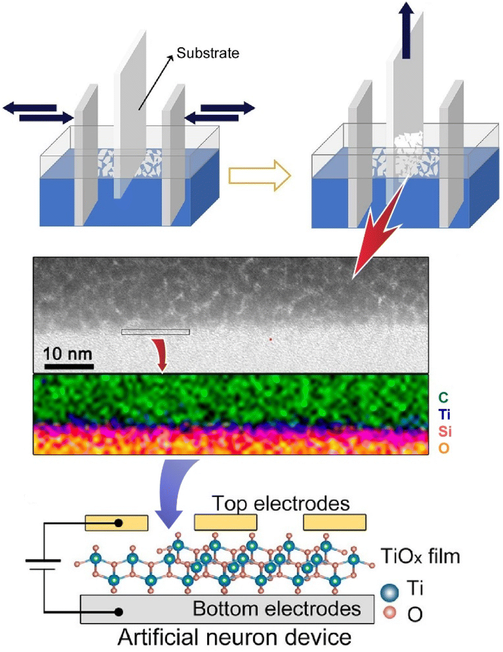 | ||
| Fig. 11 Controllable integration of solution-treated two-dimensional single-walled titanium oxide nanosheets to produce ultra-thin, sub-10 nm size two-dimensional oxide-based artificial neuron systems. Reproduced with permission from ref. 74. Copyright 2021 American Chemical Society. | ||
In this section, it is shown that various oriented nanomaterials can be assembled and organized at the liquid interface. Various inorganic nanomaterials, which do not necessarily have amphiphilic properties, can be organized two-dimensionally by LB and related methods. Such inorganic nanomaterials have various functions, and their thin-film assemblies are being actively investigated as electrochromic devices, light-emitting diodes, gas sensors, various batteries, capacitors, and artificial neuron devices. Nanoarchitectonics on liquid surfaces is a useful method to fabricate functional materials and devices with inorganic nanomaterials and their hybrids.
4. Metal–organic frameworks (MOFs) and covalent organic frameworks (COFs)
At the air–liquid interface, substances that dissolve in the liquid meet substances that do not dissolve in the liquid. At the liquid–liquid interface, substances that are soluble in their respective liquids can encounter. Therefore, liquid interfaces provide opportunities that two-dimensional thin-film structures are produced through specific interactions such as hydrogen bonding, metal coordination, and covalent bonding between different components. The liquid interface sometimes becomes an ideal environment for nanoarchitectonics for supramolecular polymers,75 metal–organic frameworks (MOFs),76 covalent organic frameworks (COFs),77 and related structures.The rational nanoarchitectonics of covalently or non-covalently bonded organic two-dimensional nanosheets is an attractive research target because of their potential applications in electronics, membrane technology, catalysis, sensing, and energy technology. Feng and co-workers synthesized triphenylene-fused nickel bis(dithiolene) complexes.78 With these complexes free-standing two-dimensional supramolecular polymer-sheets (0.7–0.9 nm thick and millimeter-level area) were successfully prepared by the LB method. The advanced complexation of nickel with thiol groups plays an important role in the strong coupling of 1,2,5,6,9,10-triphenylenehexathiol (THT) monomer units in the polymer nanosheets. This two-dimensional supramolecular polymer nanosheet (THTNi) immobilized on the electrode surface exhibited excellent electrocatalytic performance in the electrocatalytic hydrogen evolution reaction (HER). The observed HER performance could be superior to those of the reported carbon nanotube based molecular catalysts and heteroatom-doped graphene catalysts. The presented strategy is expected to activate the development of new free-standing organic two-dimensional materials with potential for application as novel electrode materials for energy applications.
MOFs are porous, crystalline metal complex networks that are structurally and functionally diverse and are often electrically insulating. Some MOF materials that exhibit high electrical conductivity while maintaining their porous nature have recently been developed.79 The usefulness of electron-active MOFs is effectively demonstrated when they are prepared in the thin-film state. Two-dimensional nanoarchitectures are often required for key applications such as chemical resistance sensors, supercapacitors, and electrocatalysts. The morphology of thin films, including crystallinity, thickness, density, roughness, and orientation, sensitively affects the device performance. Precise control of such morphological parameters remains a major challenge to be addressed. Makiura and co-workers have developed a conductive MOF nanosheet composed of 2,3,6,7,10,11-hexaiminotriphenylene molecules and nickel ions (HITP–Ni–NS).80 HITP–Ni–NS was prepared by applying air–liquid interface bottom-up synthesis (Fig. 12). The high crystallinity and uniaxial orientation of HITP–Ni–NS were revealed by synchrotron X-ray crystallography. Since HITP–Ni–NS synthesized at the air–liquid interface can be easily transferred to any substrate, its electrical conductivity was measured and found to be 0.6 S cm−1. The observed value is sufficiently high among nanosheets composed of the same type of molecule. In addition, the light transmittance of the nanosheet was evaluated and found to be 99% in the visible light range, indicating that it has extremely high light transmittance capacity. Many conductive materials, such as graphite and conductive polymers, are known to have a dark color such as black due to their conductive electron properties. They are essentially in states of low light transmittance. Unlike known materials, the newly nanoarchitected nanosheet is extremely thin and achieves high light transmittance despite its conductive nature. Such conductive materials with high light transmittance are useful as electrodes for displays and solar cells.
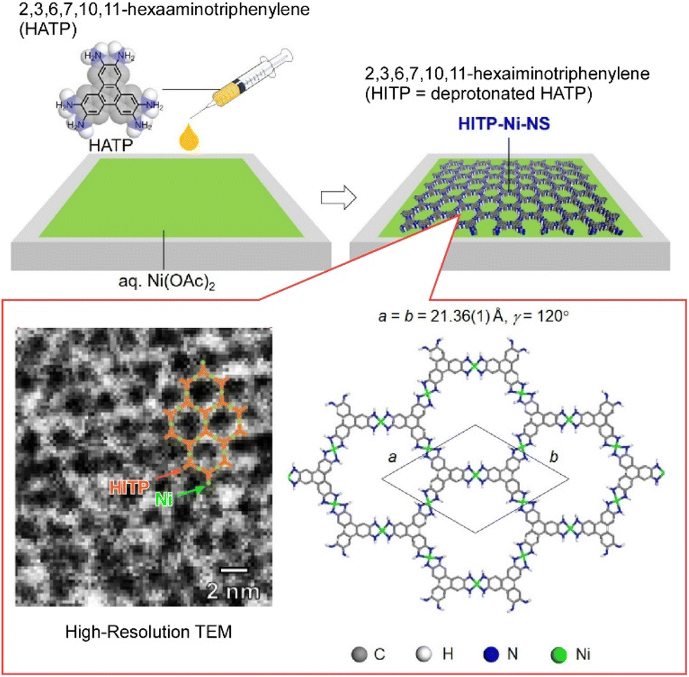 | ||
| Fig. 12 Fabrication of a conductive MOF nanosheet composed of 2,3,6,7,10,11-hexaiminotriphenylene molecules and nickel ions at the air–water interface. Reproduced with permission from ref. 80. Copyright 2021 American Chemical Society. | ||
In the nanosheet obtained in the above-mentioned research, the honeycomb structures and the stacked motifs are oriented and properly connected, which is thought to result in smooth charge transfer and high electrical conductivity. The successfully fabricated porous and conductive nanosheets are expected to accelerate the development of sensors and batteries with higher functionality and smaller size. In particular, conductive nanosheets are expected to be used as molecular sensors with a simple device structure. In the nanosheet nanoarchitectonics at the water surface, it is possible to change the shape and size of the pores through appropriate selection of the component units. By designing the appropriate pore for each sample, the selectivity of the sample can be improved. Since the uptake of the guest materials into the pore affects the electrical conductivity of the nanosheet, the guest detection sensitivity can be expected. In addition, the nanosheets obtained in this study are expected to effectively incorporate and release molecules and ions into the pores. Therefore, the nanosheets may be applied to electrodes of energy storage devices such as thin-film batteries and thin-film capacitors to realize faster charge–discharge and higher charge capacity.
COFs are a class of polymers in which organic units are covalently bonded to form ordered structures, providing an irreplaceable platform for organic and polymeric materials design.81 As emphasized in a recent review article by Jiang,82 the key question is how to express the functions and properties specific to COFs. In this context, it is increasingly important to understand and synthetically control the interactions with photons, excitons, phonons, electrons, holes, ions, spins, and molecules. Direct fabrication of COF films is an effective way to overcome the limitation of COFs’ low solubility, as mentioned in the review paper by Wang and co-workers.83 Their review paper outlines the synthesis of COF films at the interface and their applications. In addition to the synthesis strategies for preparing monolayer COFs with large crystalline domains on solid substrates, interfacial synthesis methods such as solid–liquid, liquid–liquid, and liquid–gas interfaces of various COF films are discussed. It would also be valuable to construct multifunctional COF membranes that take advantage of the various properties of COFs.
Zhang et al. synthesized two-dimensional covalent organic monolayers from simple aromatic triamine and dialdehyde building blocks by dynamic imine chemistry at the air–water interface (Fig. 13).84 The monolayers transferred by the LB method were characterized as ultrathin aromatic polyimine nanosheets. Considering the modularity of imine formation and the wide substrate range, the work reported here opens many new possibilities for the systematic exploration of the synthesis of customizable two-dimensional polymers. In particular, the formation of such smooth, coherent, large, and freestanding polyimine monolayers can represent a major step toward the preparation of conjugated two-dimensional polymers for electronic and optoelectronic applications.
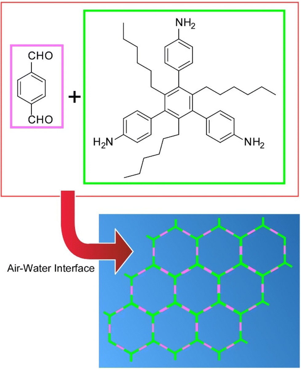 | ||
| Fig. 13 Synthesis of two-dimensional covalent organic monolayers from aromatic triamine and dialdehyde building blocks by dynamic imine chemistry at the air–water interface. | ||
COF materials would be highly suitable nanoarchitectures for membrane applications because they can have high flux and high selectivity as separation membranes. Lai and co-workers have synthesized crystalline two-dimensional COF membranes from two precursors, 1,3,5-triformylphloroglucinol (TFP) and 9,9-dihexylfluorene-2,7-diamine (DHF) using the LB technique at the air–water interface (Fig. 14).85 The condensation reaction between TFP and DHF involves two steps. The first step is a reversible Schiff's base condensation between the amine and aldehyde groups, producing an enol–imine structure. The second step is an irreversible tautomeric reaction, producing a β-ketoenamine structure. A single COF layer is exactly four unit cells thick, and each layer can be transferred to a different support surface. TFP–DHF two-dimensional COF membranes supported on anodic aluminum oxide porous supports were found to exhibit remarkable permeability to polar and nonpolar organic solvents. The observed performances are approximately 100 times higher than amorphous membranes prepared by the same procedure and comparable to the highest levels of known polymeric membranes. The transport mechanism through the COF membrane can be assigned to an enhancement of viscous flow and a strong slip boundary, as different from the amorphous polymer membrane. The membranes were found to exhibit sharp molecular sieving with a molecular weight retention onset of about 600 Da and a molecular weight cutoff of about 900 Da. This improved performance is attributed to the structural change from an amorphous structure to a well-defined ordered porous structure, clearly indicating the high potential of two-dimensional COF as a next-generation membrane material. The membranes have permanent pores and do not require pore activation. These results demonstrate the great potential of two-dimensional COF membranes in high-performance organic solvent nanofiltration applications.
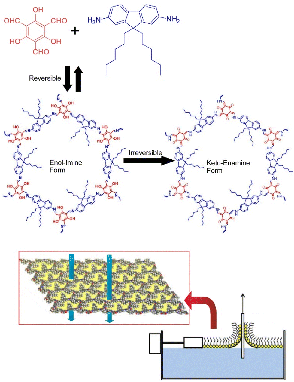 | ||
| Fig. 14 Synthesis of crystalline two-dimensional COF membranes from two precursors, 1,3,5-triformylphloroglucinol and 9,9-dihexylfluorene-2,7-diamine using the LB technique at the air–water interface. Reproduced with permission from ref. 85. Copyright 2018 American Chemical Society. | ||
Although the advantages of high fluxing of COF membranes have been demonstrated, the ability of easy structural modification to manipulate the pore size has not yet been fully explored. Lai and co-workers used the LB method to synthesize a COF membrane with a similar backbone structure, but with different carbon chain lengths.86 The latter structural modification can lead to reasonable control of the pore size. By varying the length of the alkyl chains (n-propyl/n-hexyl/n-nonyl), the pore size of the COF films was tuned to 1.72, 1.41, and 1.22 nm. Membrane permeation experiments for organic solvent nanofiltration and molecular sieving of organic dyes confirmed that the membrane flux and molecular weight cutoffs systematically correlated with changes in the pore size. Pore engineering of COF membranes can be made with the tunability of the compositions. Precise control of pore shape, size, and chemistry could dramatically enhance the functionality of COF membranes in many applications.
This section presents examples of the synthesis of well-defined functional structures such as MOFs and COFs at the liquid interface. The liquid–liquid interface is the medium where the insoluble and dissolved components of a solution can encounter, and the liquid–liquid interface offers opportunities where the dissolved components of each liquid layer can interact. It can be regarded as a very favourable environment for synthesizing MOFs by coordination bonding and COFs by covalent bonding as porous two-dimensional materials. Although simple in principle, a wide variety of two-dimensional materials can be synthesized. By selecting the constituents, functions such as conductivity can be obtained, and functions such as excellent transparency can be obtained due to the fact that the film is very thin. Nanofiltration applications are also being considered because of the two-dimensional ultra-thin film with an array of precisely designed nanopores. MOF and COF fabrication at the liquid interface is expected to play an important role in the development of various functional structures.
5. Organic semiconductors
Molecules often see functional breakthroughs when they take on an aggregate structure rather than stand-alone. In order to achieve higher functionality, it is necessary to take a high quality organized structure. For this purpose, it is often advantageous for molecules to be ordered in a two-dimensional plane, such as in a molecular thin film, rather than spread out in a three-dimensional organized structure. For example, when organic semiconductor molecules are made into an ordered structure within a two-dimensional molecular thin film, their electrical properties change drastically.87 As an example of the importance of the two-dimensional organization of functional molecules, several examples of the development of two-dimensional organic semiconductor thin films are summarized in this section. These examples are mainly selected from recent works by Watanabe, Takeya, and co-workers.88Recently, Kasuya et al. revealed for the first time that a metallic state is realized in organic semiconductor two-dimensional crystals.89 It is known that dense injection of electrons and holes into an insulating and/or semiconductive material can change it from an insulator to a metal-like state. The insulator-to-metal transition has also been theoretically studied for organic semiconductor crystals for a long time, but has not been experimentally demonstrated. This was due to the difficulty of producing extremely pure organic semiconductor thin films that are free of defects. This research group has developed a method to fabricate organic semiconductor single-crystal thin films with a thickness of a few molecular layers by a printing process (Fig. 15). Organic semiconductor 3,11-dioctyldinaphtho[2,3-d:2′,3′-d′]benzo[1,2-b:4,5-b′]dithiophene (C8-DNBDT) thin films were obtained using this method. The surface of the C8-DNBDT thin film is free of the slightest defect. The number of molecular layers in the film is precisely controlled, making it an ideal film for demonstrating the insulator–metal transition. Using such a high-quality thin film surface, an electric double layer transistor (ELDT) was fabricated. When a high density of holes, equivalent to one charge per four molecules, was introduced into C8-DNBDT, a low sheet resistance of 17 kW at 260 K was observed. This value is about one order of magnitude lower than that obtained using a typical field-effect transistor, and is sufficiently small compared to the quantized resistance, which is a measure of the insulator–metal transition. The sheet resistance of the C8-DNBDT thin film shows a monotonically decreasing temperature dependence down to temperatures as low as 10 K due to the realization of high-density carrier injection. These observations demonstrated that the metallic state has been realized in organic semiconductor crystals. The temperature dependence of carrier mobility obtained by Hall effect measurement is consistent with the standard model of two-dimensional electron systems, indicating the formation of a two-dimensional hole gas with the charge confined to the thickness of a single molecular layer in this system. This research is expected to accelerate applications to high-speed electronic devices and quantum electronic devices.
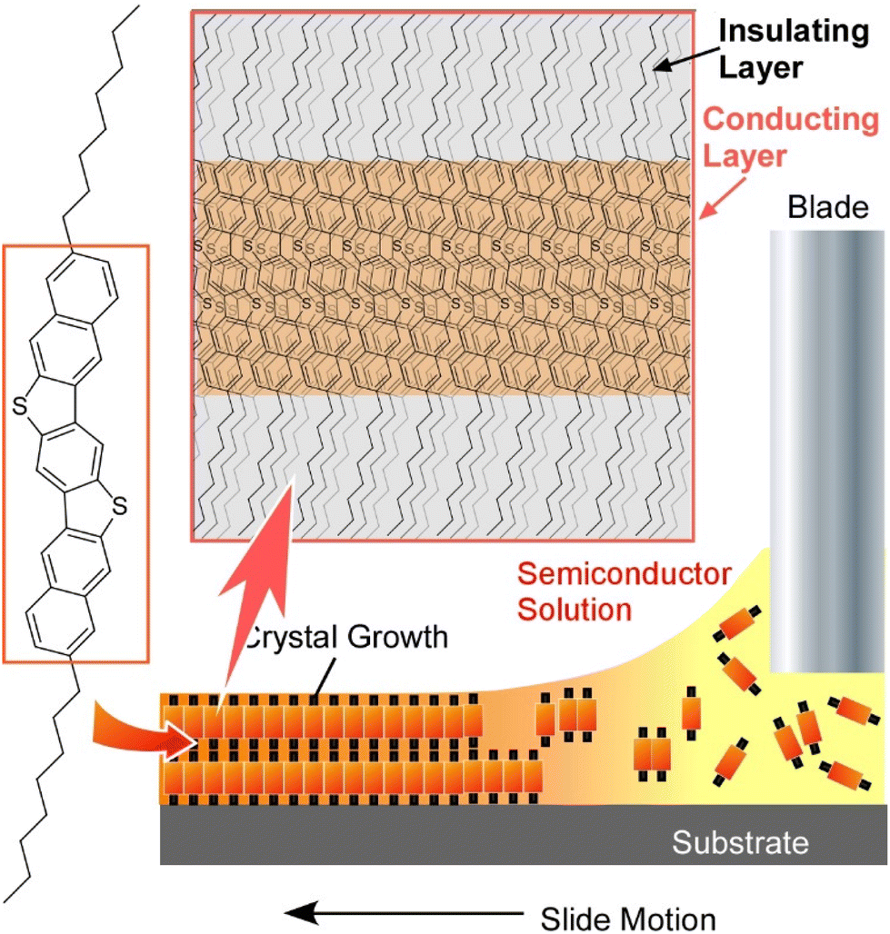 | ||
| Fig. 15 Fabrication of the organic semiconductor (3,11-dioctyldinaphtho[2,3-d:2′,3′-d′]benzo[1,2-b:4,5-b′]dithiophene, C8-DNBDT) single-crystal thin films with a thickness of a few molecular layers by a printing process. | ||
Makita et al. reported a water-based film transfer method using an organic semiconductor, (3,11-dinonyldinaphtho[2,3-d:2′,3′-d′]benzo[1,2-b:4,5-bI]dithiophene) (Fig. 16).90 In the initial step, organic semiconductor single-crystal ultrathin films with a thickness of only a few molecular layers (about 10 nm) were deposited on natural mica using a printing method that enables large-area fabrication of nanofilms. Natural mica is known for its atomic-level flatness and superhydrophilic surface nature. By immersing the entire mica substrate in water after film formation, the semiconductor ultra-thin film peels off from the substrate and floats in water. The floating of the ultra-thin film in water is thought to be caused by the difference in affinity for water between the superhydrophilic natural mica surface and the highly hydrophobic organic semiconductor film surface. This difference in surface hydrophilicity allows water to penetrate into the interface between the natural mica and organic semiconductor film. The obtained ultrathin film retains its original single-crystalline nature with a value of mobility corresponding to a high-quality single-crystalline semiconductor film, exceeding 10 cm2 V−1 s−1.
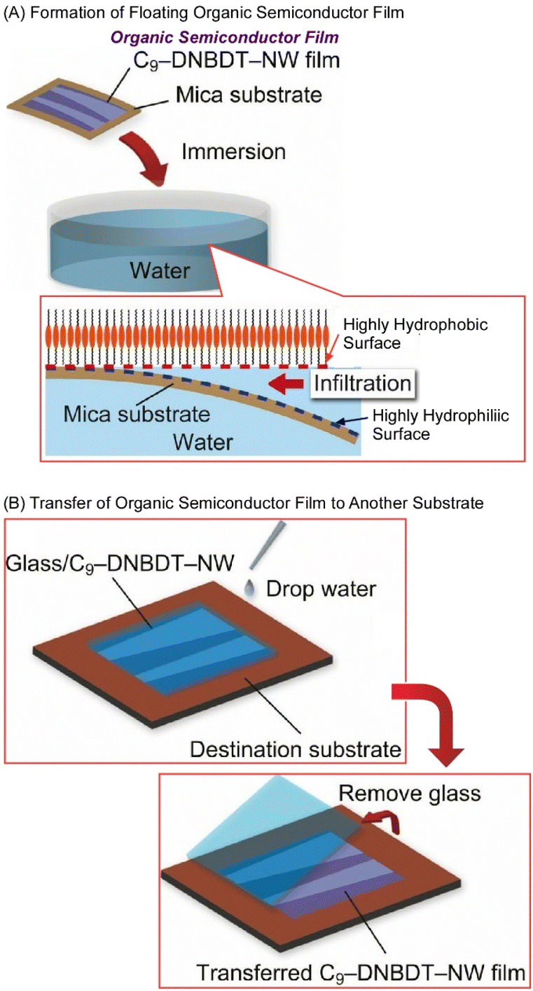 | ||
| Fig. 16 Water-based film transfer method using an organic semiconductor: (A) formation of a floating organic semiconductor film; (B) transfer of the organic semiconductor film to another substrate. Reproduced from ref. 90, under the terms of the CC BY. | ||
Similarly, the semiconductor film printed on a superhydrophilic substrate can be peeled off from the substrate upon dropping water. The peeled semiconductor thin film can be subsequently transferred to another substrate just by contact. Because this method is a simple process using only water, it is now possible to attach organic semiconductor ultra-thin films to a variety of material surfaces that were previously incompatible with the printing method. For example, organic thin-film transistors (OTFTs) can be fabricated even on fluoropolymer surfaces and food wraps, which have been generally difficult to use with conventional procedures. The ability to choose from such a wide variety of substrates will greatly expand the potential applications of organic semiconductor devices in the future. Because the transfer of organic semiconductor ultra-thin films in the sufficiently largest area is possible, this method can be adapted to practical mass production processes. It can also be applied to high-performance multilayer devices, which are difficult to achieve using conventional technologies.
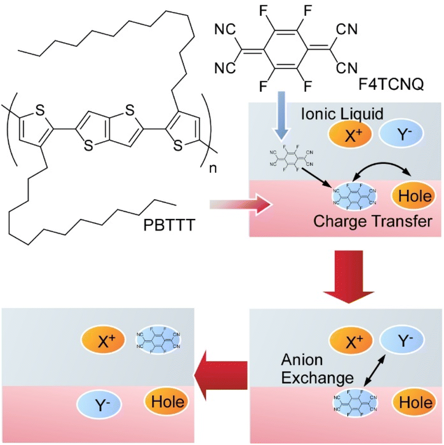
Polymeric organic semiconductors can dramatically change the number of electrons by redox reactions with added dopant molecules, often making them conductive polymers. However, dopant molecules with strong redox ability are usually sensitive to water and oxygen in the atmosphere, easily losing their function as dopants. Yamashita et al. proposed a new method of ion exchange by the addition of the second ions to the conventional bimolecular doping system (Fig. 17).91 This method eliminates the limitations that could not be escaped in the bimolecular doping system and results in a conductive polymer with a much higher conductivity than before. They actually succeeded in developing conductive polymers with conductivity significantly higher than that of conventional bimolecular systems. It was experimentally confirmed that ionized dopant molecules instantly exchange with newly added ions, and surprisingly, by selecting appropriate ions, the ion conversion efficiency has also become almost 100%. The model case for this study was demonstrated by exchange of the initial dopant 2,3,5,6-tetrafluoro-7,7,8,8-tetracyanoquinodimethane (F4TCNQ) by the second dopant bis(trifluoromethylsulfonyl)imide (TFSI) in well-used polymeric semiconductor films of poly[2,5-bis(3-tetradecylthiophen-2-yl)thieno[3,2-b]thiophene] (PBTTT). Exposure of F4TCNQ-doped PBTTT thin films to ionic liquid 1-ethyl-3-methylimidazolium bis(trifluoromethylsulfonyl)imide (EMIM-TFSI) induced dopant exchange to TFSI ions with almost 100% conversion efficiency based on minimization of free energy between the polymer organic semiconductor and the dopant. Highly doped polymer organic semiconductors also exhibit temperature dependence of electrical resistance similar to metals. The regular arrangement of the polymer chains with the dopants introduced by ion exchange results in the electrons leaving the polymer chains and behaving like waves as seen in the electronic state of common metals. The proposed method is a solution process at room temperature that can be easily applied to large areas. The process significantly improves the doping levels, crystallinity, thermal durability, and conduction properties of polymeric organic semiconductors. The selection of a variety of ionic compounds will enable further control of the conduction and physicochemical properties.
 | ||
| Fig. 17 A method of ion exchange by the addition of the second ions to the organic semiconductor thin film. | ||
Compared to small molecule organic semiconductors, the crystallization of polymeric organic semiconductors is not always easy. In order to achieve high performance polymer organic semiconductor films, it is necessary to improve the quality of the films, such as their orientation and packing. In some cases, film deposition processes at high temperatures are required.92 As seen in the conventional LB method, molecules deployed on the surface of water are known to spread quickly to form ultra-thin film-like aggregates at the molecular level.93 Development of devices using precisely aligned molecules is actively underway. However, the liquid used in the conventional LB method is mainly limited to water, and the use of the LB method has been restricted to processes at room temperature to avoid disturbance by water vapor pressure. Ito et al. developed the ultra-high temperature LB process, using ionic liquids as subphase liquids, which remain in a liquid state even at high temperatures with almost zero vapor pressure, for the LB method at temperatures above 100 °C (Fig. 18).94 Using ultra-high temperature LB instruments, fabrication of high-quality ultrathin films of polymeric organic semiconductors were actually demonstrated. This high-temperature LB method was applied to polymeric organic semiconductors that may require ultra-high temperature processes above 100 °C. The successful formation of homogeneous nanofilms over a large area of more than 1 cm2 with high crystallinity was demonstrated. The newly developed ultra-high temperature LB method and its manufacturing equipment can significantly expand the processable temperature range while maintaining the concept of forming precise molecular aggregates on the liquid surface. This enables the formation of various molecular assemblies that have not been studied due to process temperature limitations, and is expected to accelerate research into molecular electronics and bioelectronic applications.
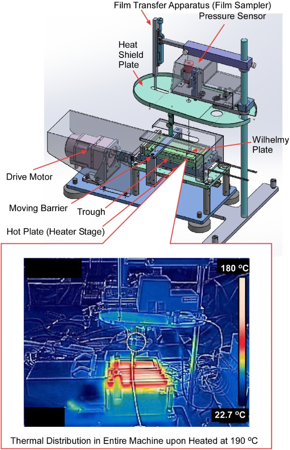 | ||
| Fig. 18 Ultra-high temperature LB instruments with actual thermal distributions (below) upon heating at 190 °C. Reproduced with permission from ref. 94. Copyright 2022 American Chemical Society. | ||
The arrangement and packing of molecules are reflected in the functionality of the entire two-dimensional materials. As examples of such features, this section summarizes research on the fabrication and function of molecular thin films of organic semiconductors. Organic semiconductors are mostly applied on solid substrates as devices, and fabrications on liquid surfaces have not been studied much. While the liquid interface is smooth at the molecular level, there is no strong interaction from the substrate, etc., and it is expected that the properties of the molecules themselves will be utilized for integration and organization while flowing. As breaking common sense in the LB technology, new attempts have been made to increase the operating temperature range to nearly 200 °C. This innovative method is useful to successfully fabricate high quality LB films. However, there is still ample room for development in the corresponding fields.
6. Proteins and stem cells
Molecular assembly in confined spaces sometimes provides technical benefits such as crystallization of useful substances. X-Ray crystallography and other methods are used to analyse the precise structure of molecules. It is not always easy to prepare crystals for this purpose, although new methods are being devised, such as the crystal sponge method by Fujita et al.95 Confined spaces, such as interfaces, become sometimes useful sites for the crystallization of functional molecules. Crystallization and structural analysis of bio-related molecules are of particular interest to the pharmaceutical industry and life sciences. Pechkova and Nicolini have proposed the LB nanotemplate method as a crystallization approach that can be used for any kind of protein (including membrane proteins).96 Highly ordered two-dimensional protein monolayers can be prepared at the air–water interface by the LB method. Subsequently, such thin films can be used as two-dimensional templates to form three-dimensional protein crystals by the hanging-drop vapor diffusion method. LB crystals were prepared only at 1–10 days and were more ordered than those produced using other crystallization methods.Not only crystallization, but also the liquid interface is a site for the two-dimensional accumulation of proteins. For example, an enzyme (glucose oxidase) modified with lipid can be assembled across the air–water interface as a monolayer without causing denaturation.97 By transferring such a monolayer onto an electrode, a sensor for glucose detection can be fabricated. The immiscible liquid–liquid interfaces also work as media appropriate for two-dimensional protein accumulation. Jia et al. demonstrated the formation of high quality two-dimensional protein films at the liquid interface between perfluorocarbon liquid and cultured aqueous solution, where interactions between the protein films and living cells such as human mesenchymal stem cells were investigated.98 Self-assembled single-molecule protein nanosheets at the fluid interface were demonstrated to be sufficiently rigid to support cell spreading without additional processing. By fine packing these proteins at the fluid interface, the dynamics of the protein layer can be tuned, ultimately allowing for controlled cell spreading. The high stiffness of protein nanosheets causes cell diffusion, adhesive growth, and nuclear migration of associated proteins. The free-standing ultrathin protein nanosheets are very flexible and easily deformable, and cells perceive them as much softer. This finding is expected to provide a new perspective for understanding cell–material interactions.
Fig. 19 shows an in situ fluorescence micrograph of fluorescein isothiocyanate-labelled bovine serum albumin assembled at the interface between perfluorocarbons and water. Perfectly smooth large-area protein nanosheets covering the entire interface were observed. When perfluorodecalin (PFD) and perfluorotributylamine (PFTBA) were used as perfluorocarbons, the thicknesses of the protein films were 2.78 ± 0.19 nm and 6.36 ± 0.12 nm, respectively, as analysed by the atomic force microscopy (AFM) observation. These values correspond to the theoretical monolayer thicknesses when serum albumin proteins of 3–6 nm diameter are accumulated in different orientations. The surface is uniform with root mean square (rms) roughness in the subnanometer range (perfluorodecalin: 0.62 ± 0.11 nm, perfluorotributylamine: 0.49 ± 0.13 nm). This study demonstrates that pure protein-based two-dimensional membranes of macroscopic dimensions consisting of molecular monolayers can be fabricated at the water–perfluorocarbon interface. In addition, the interactions between cells and protein thin films at the fluid interface can be explained in the framework of the molecular clutch model. Cell culture at the liquid interface is expected to facilitate the development of next-generation stem cell culture materials and implant interfaces to enhance the effectiveness of regenerative therapies.
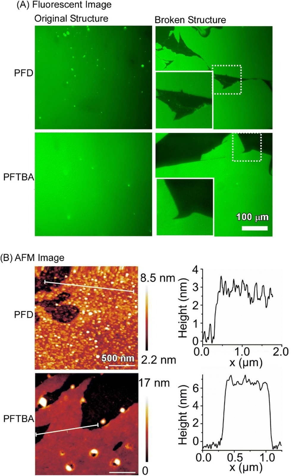 | ||
| Fig. 19 (A) Fluorescence images and (B) AFM images of fluorescein isothiocyanate-labelled bovine serum albumin assembled at the interface between perfluorocarbons (perfluorodecalin (PFD) and perfluorotributylamine (PFTBA)) and water. Reproduced with permission from ref. 98. Copyright 2019 Wiley-VCH. | ||
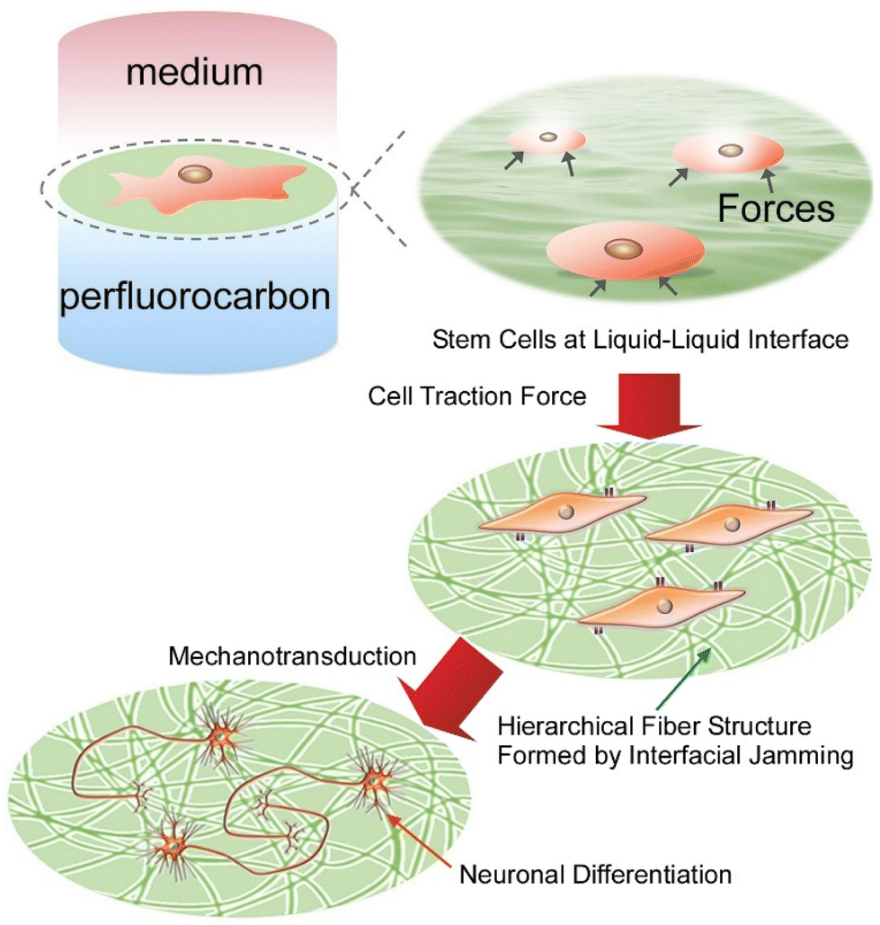
Stem cells and iPS cells play a central role in the fields of regenerative medicine and tissue engineering. Until now, expensive differentiation inducing factors such as cytokines have generally been used, but this has been problematic from a cost perspective. Jia et al. demonstrated that a protein monolayer formed at the interface between perfluorocarbon and water is able to adapt dynamically to the traction force of cells.99 The protein monolayer (such as fibronectin layer) can induce cell differentiation as a tuneable adaptive material through dynamically regulating cell traction (Fig. 20). Interfacial jamming causes structural changes in protein films from monolayers to hierarchical fibers. Elongated fibronectin fibers promote the formation of elongated cell adhesion structures, increase the activation of cell adhesion kinases, and promote neural differentiation of stem cells. Mesenchymal stem cells cultured on the interface between perfluorocarbon and water spontaneously differentiated into neurons without the addition of differentiation inducing factors. It was found that the liquid–liquid interface provided flexible characteristics to the protein films, which transformed and accumulated in response to the force exerted by the stem cells, thereby promoting efficient differentiation into nerve cells.
 | ||
| Fig. 20 Induction of cell differentiation through dynamically regulating cell traction by the protein monolayer formed at the interface between perfluorocarbon and water. Reproduced with permission from ref. 99. Copyright 2020 Wiley-VCH. | ||
Physical reorganization and nanoscale spatial rearrangement of fibronectin at the liquid–liquid interface resulted in a hierarchical fiber structure of fibronectin aggregates adjacent to mesenchymal stem cells. This fiber structure was transferred to mesenchymal stem cells by the spatial arrangement of adhesion plaques, leading to the achievement of optimal cytoskeletal tension and promoting neurogenesis. Thus, cellular traction caused a spatial rearrangement of extracellular matrix proteins that induced membrane receptor clustering, activated signalling pathways, and ultimately altered stem cell fate. These results will help to elucidate the dynamics of the extracellular matrix, biological signalling, and feedback mechanisms linking long-term stem cell fate. These findings will contribute broadly to applications in tissue engineering and regenerative medicine. This has great potential as an efficient and inexpensive differentiation induction technology, which is important in regenerative medicine technology using stem cells. In the future, the demonstrated methodology is expected to be utilized for the differentiation of not only nerves but also various other types of cells. Two-dimensional nanoarchitectonics with proteins and living cells would make a further leap forward as a material-based regenerative medicine technology.
As a final frontier, the control of biomolecules and stem cells at liquid interface fields is reported in this section. Although biomaterials are incompatible with normal organic solvents and may denature, perfluorocarbons are not so harmful to biomaterials and cells. Perfluorocarbon solvents can be used as liquid phases in biological research. At the interface between water and perfluorocarbon, proteins accumulate as a neat two-dimensional thin film, which interacts with cells with weak forces. These phenomena include many characteristics that have not been observed in normal culture on solid substrates. There are many unknowns remaining in this field where future research development is much expected.
7. Summary and perspectives
The synthesis of functional materials with reasonable nanostructures requires the integration of knowledge of nanotechnology with other fields of materials science. The new concept of nanoarchitectonics will play this role, establishing a methodology for assembling functional materials from nano units (atoms, molecules, and nanomaterials). It is usually difficult to directly assemble complex systems in an unrestricted three-dimensional structure. A better and more realistic way is to assemble functional systems in a confined environment such as interfaces. Although various nanotechnology and nanoarchitectonics have been performed on solid substrates, the corresponding attempts on liquid surfaces have not been sufficiently investigated. While observation and analysis methods for atomic/molecular-level structures and properties have been developed at the solid interfaces, these strategies cannot be usually applied to systems on a liquid because of large fluctuations in liquid media. Accordingly, nanoarchitectonic research in liquid interface fields has been lagging behind. However, there are many advantages at liquid interfaces that cannot be considered at solid interfaces. The liquid interface is a fluctuating but spontaneously regulated interface at the molecular level. Dynamic stimuli can be easily applied by compressing the film from the lateral direction or by flowing the liquid layer. No mechanical constraints from the solid substrate. It can be a field where materials with different solubility in the liquid phase are brought into contact, and it can be a field possibly with specific structure formation and reactions within a two-dimensional plane. As exemplified in this paper, a wide range of materials can be organized and functionalized on liquid interfaces, including organic molecules, inorganic nanomaterials, hybrids, organic semiconductor thin films, proteins, and stem cells. Two-dimensional nanocarbon sheets have also been fabricated by molecular reactions at dynamically moving interfaces, and MOF and COF films have been fabricated by specific interactions and reactions at the interface. Thus, the potential for the fabrication of functional materials in two-dimensional nanospaces at liquid surfaces (two-dimensional world within a nanoscale distance from the liquid phase) is sufficiently high. Therefore, functions such as sensors, devices, energy-related applications, and cell control are being explored.Nanoarchitectonics on liquids has possibilities not found in the functional expression of solids and should be studied more intensively. Molecular assembly on a liquid is expected to be uniquely advantageous for dynamic functional expression involving conformational changes, since there are no strong restrictions from the solid substrate. The energy or force exerted for monolayer compression on a liquid is much smaller than that exerted by light irradiation and the other external stimuli.100 Rather, it is only used to change the soft conformation of the molecule. Therefore, on the liquid surface, we can expect to develop functions through delicate conformational changes of the molecules. In biological systems, there are huge numbers of examples of delicate conformational changes in biomolecules by weak forces under thermal fluctuations during function expressions. In artificial systems, it is also possible to optimize the molecular recognition capability by structurally tuning molecular receptors at the air–water interface.101 Functional exploration through delicate structural tuning of molecules is an unexplored and challenging area, and the methodology of nanoarchitectonics on the liquid surface will pave the way for such exploration. On the liquid surface, it is expected that assemblies are formed in such a way that the movement of individual components is tolerated. Thus, it may be possible to fabricate functional structures in which many molecular components can interact and communicate with each other. This is analogous to the case of many proteins and functional molecules working in tandem on a cell membrane.102
Nanoarchitectonics on liquids has the potential to create such multi-component functional material systems with integrated functions. Of course, these structures and functional systems are also expected to be fixed on devices as thin films. Prediction of complex and advanced functional manifestations will require the integration of new concepts such as materials informatics.103 Nanoarchitectonics is an open concept and is expected to sufficiently evolve as new concepts and methodologies for future challenges.
Author contributions
It is a single author paper. The author performed all the tasks.Conflicts of interest
There are no conflicts to declare.Acknowledgements
This study was partially supported by JSPS KAKENHI Grant Number JP20H00392, JP20H00316 and JP21H04685.Notes and references
- (a) G. Povie, Y. Segawa, T. Nishihara, Y. Miyauchi and K. Itami, Science, 2017, 356, 172 CrossRef CAS PubMed; (b) Z. Sun, K. Ikemoto, T. M. Fukunaga, T. Koretsune, R. Arita, S. Sato and H. Isobe, Science, 2019, 363, 151 CrossRef CAS PubMed; (c) T. P. Stockdale, N. Y. S. Lam, M. J. Anketell and I. Paterson, Bull. Chem. Soc. Jpn., 2021, 94, 713 CrossRef CAS; (d) H. L. Anderson, C. W. Patrick, L. M. Scriven and S. L. Woltering, Bull. Chem. Soc. Jpn., 2021, 94, 798 CrossRef CAS.
- (a) A. Kudo and Y. Misekia, Chem. Soc. Rev., 2009, 38, 253 RSC; (b) B. Singh, J. Na, M. Konarova, T. Wakihara, Y. Yamauchi, C. Salomon and M. B. Gawande, Bull. Chem. Soc. Jpn., 2020, 93, 1459 CrossRef CAS; (c) G. Singh, J. M. Lee, G. Kothandam, T. Palanisami, A. H. Al-Muhtaseb, A. Karakoti, J. Yi, N. Bolan and A. Vinu, Bull. Chem. Soc. Jpn., 2021, 94, 1232 CrossRef CAS; (d) D. Wu, K. Kusada, Y. Nanba, M. Koyama, T. Yamamoto, T. Toriyama, S. Matsumura, O. Seo, I. Gueye, J. Kim, L. S. R. Kumara, O. Sakata, S. Kawaguchi, Y. Kubota and H. Kitagawa, J. Am. Chem. Soc., 2022, 144, 3365 CrossRef CAS PubMed.
- (a) M. Kamigaito, T. Ando and M. Sawamoto, Chem. Rev., 2001, 101, 3689 CrossRef CAS PubMed; (b) M. Gon, S. Ito, K. Tanaka and Y. Chujo, Bull. Chem. Soc. Jpn., 2021, 94, 2290 CrossRef CAS; (c) E. Yashima and K. Maeda, Bull. Chem. Soc. Jpn., 2021, 94, 2637 CrossRef CAS; (d) Y. Higaki and A. Takahara, Polym. J., 2022, 54, 473 CrossRef CAS.
- (a) K. Ariga, M. Nishikawa, T. Mori, J. Takeya, L. K. Shrestha and J. P. Hill, Sci. Technol. Adv. Mater., 2018, 20, 51 CrossRef PubMed; (b) S. Datta, Y. Kato, S. Higashiharaguchi, K. Aratsu, A. Isobe, T. Saito, D. D. Prabhu, Y. Kitamoto, M. J. Hollamby, A. J. Smith, R. Dalgliesh, N. Mahmoudi, L. Pesce, C. Perego, G. M. Pavan and S. Yagai, Nature, 2020, 583, 400 CrossRef CAS PubMed; (c) T. Kato, M. Gupta, D. Yamaguchi, K. P. Gan and M. Nakayama, Bull. Chem. Soc. Jpn., 2021, 94, 357 CrossRef CAS; (d) V. Percec and Q. Xiao, Bull. Chem. Soc. Jpn., 2021, 94, 900 CrossRef CAS.
- (a) R. Sakamoto, K. Hoshiko, Q. Liu, T. Yagi, T. Nagayama, S. Kusaka, M. Tsuchiya, Y. Kitagawa, W.-Y. Wong and H. Nishihara, Nat. Commun., 2015, 6, 6713 CrossRef CAS PubMed; (b) K. Ariga and M. Shionoya, Bull. Chem. Soc. Jpn., 2021, 94, 839 CrossRef CAS; (c) Y. Gu, J.-J. Zheng, K.-I. Otake, M. Shivanna, S. Sakaki, H. Yoshino, M. Ohba, S. Kawaguchi, Y. Wang, F. Li and S. Kitagawa, Angew. Chem., Int. Ed., 2021, 60, 11688 CrossRef CAS PubMed; (d) H. Takezawa and M. Fujita, Bull. Chem. Soc. Jpn., 2021, 94, 2351 CrossRef CAS.
- (a) W. Chaikittisilp, N. L. Torad, C. Li, M. Imura, N. Suzuki, S. Ishihara, K. Ariga and Y. Yamauchi, Chem. – Eur. J., 2014, 20, 4217 CrossRef CAS PubMed; (b) Y. Lvov, W. Wang, L. Zhang and R. Fakhrullin, Adv. Mater., 2016, 28, 1227 CrossRef CAS PubMed; (c) M. Yamashita, Bull. Chem. Soc. Jpn., 2021, 94, 209 CrossRef CAS; (d) M. S. Islam, Y. Shudo and S. Hayami, Bull. Chem. Soc. Jpn., 2022, 95, 1 CrossRef CAS.
- (a) K. Tanaka and K. Vong, Bull. Chem. Soc. Jpn., 2020, 93, 1275 CrossRef CAS; (b) Y. Watanabe, Y. Aiba, S. Ariyasu and S. Abe, Bull. Chem. Soc. Jpn., 2020, 93, 379 CrossRef CAS; (c) T. Katoh and H. Suga, Bull. Chem. Soc. Jpn., 2021, 94, 549 CrossRef CAS; (d) S. Sethi, H. Sugiyama and M. Endo, ChemBioChem, 2022, 23, e202100446 CrossRef CAS PubMed.
- (a) R. Waser and M. Aono, Nat. Mater., 2007, 6, 833 CrossRef CAS PubMed; (b) M. V. de Ruiter, R. Klem, D. Luque, J. J. L. M. Cornelissen and J. R. Castón, Nanoscale, 2019, 11, 4130 RSC; (c) J. Li, C. C. Mayorga-Martinez, C. D. Ohl and M. Pumera, Adv. Funct. Mater., 2022, 32, 2102265 CrossRef CAS; (d) K. Ariga, Small Struct., 2021, 2, 2100006 CrossRef CAS.
- (a) Y. Sugimoto, P. Pou, M. Abe, P. Jelinek, R. Pérez, S. Morita and Ó. Custance, Nature, 2007, 446, 64 CrossRef CAS PubMed; (b) X. Zhang, Q. Zeng and C. Wang, Nanoscale, 2013, 5, 8269 RSC; (c) X. Xu, K. Müllen and A. Narita, Bull. Chem. Soc. Jpn., 2020, 93, 490 CrossRef CAS; (d) T. Shimizu, D. Lungerich, J. Stuckner, M. Murayama, K. Harano and E. Nakamura, Bull. Chem. Soc. Jpn., 2020, 93, 1079 CrossRef CAS.
- (a) K. Kimura, K. Miwa, H. Imada, M. Imai-Imada, S. Kawahara, J. Takeya, M. Kawai, M. Galperin and Y. Kim, Nature, 2019, 570, 210 CrossRef CAS PubMed; (b) E. Kazuma, Bull. Chem. Soc. Jpn., 2020, 93, 1552 CrossRef CAS; (c) N. Kornienko, Nanoscale, 2021, 13, 1507 RSC; (d) F. Eisenhut, T. Kühne, J. Monsalve, S. Srivastava, D. A. Ryndyk, G. Cuniberti, O. Aiboudi, F. Lissel, V. Zobač, R. Robles, N. Lorente, C. Joachim and F. Moresco, Nanoscale, 2021, 13, 16077 RSC.
- (a) A. Bednarkiewicz, L. Marciniak, L. D. Carlos and D. Jaque, Nanoscale, 2020, 12, 14405 RSC; (b) P. Verma, Y. Kuwahara, K. Mori, R. Raja and H. Yamashita, Nanoscale, 2020, 12, 11333 RSC; (c) T. Akutagawa, Bull. Chem. Soc. Jpn., 2021, 94, 1400 CrossRef CAS; (d) N. Hosono and T. Uemura, Bull. Chem. Soc. Jpn., 2021, 94, 2139 CrossRef CAS.
- K. Ariga, Nanoscale Horiz., 2021, 6, 364 RSC.
- (a) K. Ariga, M. Li, G. J. Richards and J. P. Hill, J. Nanosci. Nanotechnol., 2011, 11, 1 CrossRef CAS PubMed; (b) K. Ariga, Q. Ji, W. Nakanishi, J. P. Hill and M. Aono, Mater. Horiz., 2015, 2, 406 RSC.
- (a) K. Ariga, Molecules, 2021, 26, 1621 CrossRef CAS PubMed; (b) K. Ariga and L. K. Shrestha, Mater. Adv., 2021, 2, 582 RSC.
- (a) R. P. Feynman, Eng. Sci., 1960, 23, 32 Search PubMed; (b) M. Roukes, Sci. Am., 2001, 285, 48 CrossRef CAS PubMed.
- (a) K. Ariga, Q. Ji, J. P. Hill, Y. Bando and M. Aono, NPG Asia Mater., 2012, 4, e17 CrossRef; (b) K. Ariga, K. Minami, M. Ebara and J. Nakanishi, Polym. J., 2016, 48, 371 CrossRef CAS.
- (a) K. Ariga, J. Li, J. Fei, Q. Ji and J. P. Hill, Adv. Mater., 2016, 28, 1251 CrossRef CAS PubMed; (b) X. Shen, J. Song, C. Sevencan, D. T. Leong and K. Ariga, Sci. Technol. Adv. Mater., 2022, 23, 199 CrossRef PubMed.
- (a) M. Ramanathan, L. K. Shrestha, T. Mori, Q. Ji, J. P. Hill and K. Ariga, Phys. Chem. Chem. Phys., 2013, 15, 10580 RSC; (b) W. Nakanishi, K. Minami, L. K. Shrestha, Q. Ji, J. P. Hill and K. Ariga, Nano Today, 2014, 9, 378 CrossRef CAS; (c) C. Tirayaphanitchkul, K. Imwiset and M. Ogawa, Bull. Chem. Soc. Jpn., 2021, 94, 678 CrossRef CAS.
- (a) L. Zhang, T. Wang, Z. Shen and M. Liu, Adv. Mater., 2016, 28, 1044 CrossRef CAS PubMed; (b) H.-X. Wang, L. Xu, X. Zhu, C. Xue, L. Zhang and M. Liu, Nanoscale, 2022, 14, 1001 RSC; (c) K. Ariga, T. Mori, T. Kitao and T. Uemura, Adv. Mater., 2020, 32, 1905657 CrossRef CAS PubMed.
- (a) H. Abe, J. Liu and K. Ariga, Mater. Today, 2016, 19, 12 CrossRef CAS; (b) N. Kumari, A. Kumar and V. Krishnan, J. Inorg. Organomet. Polym., 2021, 31, 1954 CrossRef CAS; (c) C. Huang, P. Qin, Y. Luo, Q. Ruan, L. Liu, Y. Wu, Q. Li, Y. Xu, R. Liu and P. K. Chu, Mater. Today Energy, 2022, 23, 100911 CrossRef CAS.
- (a) S. Ishihara, J. Labuta, W. Van Rossom, D. Ishikawa, K. Minami, J. P. Hill and K. Ariga, Phys. Chem. Chem. Phys., 2014, 16, 9713–9746 RSC; (b) M. Pandeeswar, S. P. Senanayak and T. Govindaraju, ACS Appl. Mater. Interfaces, 2016, 8, 30362 CrossRef CAS PubMed; (c) M. Komiyama, T. Mori and K. Ariga, Bull. Chem. Soc. Jpn., 2018, 91, 1075 CrossRef CAS.
- (a) J. M. Giussi, M. L. Cortez, W. A. Marmisollé and O. Azzaroni, Chem. Soc. Rev., 2019, 48, 814 RSC; (b) K. Ariga, M. Ito, T. Mori, S. Watanabe and J. Takeya, Nano Today, 2019, 28, 100762 CrossRef; (c) K. Terabe, T. Tsuchiya and T. Tsuruoka, Adv. Electron. Mater. DOI:10.1002/aelm.202100645 , in press.
- (a) Q. Zou, K. Liu, M. Abbas and X. Yan, Adv. Mater., 2016, 28, 1031 CrossRef CAS PubMed; (b) A. H. Khan, S. Ghosh, B. Pradhan, A. Dalui, L. K. Shrestha, S. Acharya and K. Ariga, Bull. Chem. Soc. Jpn., 2017, 90, 627 CrossRef; (c) J. Kim, J. H. Kim and K. Ariga, Joule, 2017, 1, 739 CrossRef CAS.
- (a) K. Ariga, S. Ishihara, H. Abe, M. Li and J. P. Hill, J. Mater. Chem., 2012, 22, 2369 RSC; (b) N. Boukhalfa, M. Darder, M. Boutahala, P. Aranda and E. Ruiz-Hitzky, Bull. Chem. Soc. Jpn., 2021, 94, 122 CrossRef CAS; (c) T.-A. Pham, A. Qamar, T. Dinh, M. K. Masud, M. Rais-Zadeh, D. G. Senesky, Y. Yamauchi, N. T. Nguyen and H. P. Phan, Adv. Sci., 2020, 7, 2001294 CrossRef CAS PubMed.
- (a) K. Ariga, Q. Ji, T. Mori, M. Naito, Y. Yamauchi, H. Abe and J. P. Hill, Chem. Soc. Rev., 2013, 42, 6322 RSC; (b) M. Komiyama, K. Yoshimoto, M. Sisido and K. Ariga, Bull. Chem. Soc. Jpn., 2017, 90, 967 CrossRef; (c) X. Liang, L. Li, J. Tang, M. Komiyama and K. Ariga, Bull. Chem. Soc. Jpn., 2020, 93, 581 CrossRef CAS.
- (a) J. Liu, F. Zhai, H. Zhou, W. Yang and S. Zhang, Adv. Healthcare Mater., 2019, 8, 1801300 CrossRef PubMed; (b) J. Liu, H. Zhou, W. Yang and K. Ariga, Acc. Chem. Res., 2020, 53, 644 CrossRef CAS PubMed; (c) Q. Ren, N. Yu, L. Wang, M. Wen, P. Geng, Q. Jiang, M. Li and Z. Chen, J. Colloid Interface Sci., 2022, 614, 147 CrossRef CAS PubMed.
- R. B. Laughlin and D. Pines, Proc. Natl. Acad. Sci. U. S. A., 2000, 97, 28 CrossRef CAS PubMed.
- K. Ariga and R. Fakhrullin, Bull. Chem. Soc. Jpn., 2022, 95, 774 CrossRef CAS.
- (a) K. Ariga, T. Mori and J. P. Hill, Adv. Mater., 2012, 24, 158 CrossRef CAS PubMed; (b) K. Ariga, Y. Yamauchi, T. Mori and J. P. Hill, Adv. Mater., 2013, 25, 6477 CrossRef CAS PubMed; (c) C. Fang, I. Yoon, D. Hubble, T.-N. Tran, R. Kostecki and G. Liu, ACS Appl. Mater. Interfaces, 2022, 14, 2431 CrossRef CAS PubMed.
- (a) G. Rydzek, Q. Ji, M. Li, P. Schaaf, J. P. Hill, F. Boulmedais and K. Ariga, Nano Today, 2015, 10, 138 CrossRef CAS; (b) M. Akashi and T. Akagi, Bull. Chem. Soc. Jpn., 2021, 94, 1903 CrossRef CAS; (c) K. Ariga, Y. Lvov and G. Decher, Phys. Chem. Chem. Phys., 2022, 24, 4097 RSC.
- (a) Q. H. Wang, Z. Jin, K. K. Kim, A. J. Hilmer, G. L. C. Paulus, C.-J. Shih, M.-H. Ham, J. D. Sanchez-Yamagishi, K. Watanabe, T. Taniguchi, J. Kong, P. Jarillo-Herrero and M. S. Strano, Nat. Chem., 2012, 4, 724 CrossRef CAS PubMed; (b) H. Morita, Polym. J., 2016, 48, 45 CrossRef CAS; (c) S. Ito, T. Nakamura and M. Nakagawa, Bull. Chem. Soc. Jpn., 2020, 93, 862 CrossRef CAS.
- K. Ariga, X. Jia, J. Song, J. P. Hill, D. T. Leong, Y. Jia and J. Li, Angew. Chem., Int. Ed., 2020, 59, 15424 CrossRef CAS PubMed.
- (a) K. N. Ferreira, T. M. Iverson, K. Maghlaoui, J. Barber and S. Iwata, Science, 2004, 303, 1831 CrossRef CAS PubMed; (b) Y. Umena, K. Kawakami, J.-R. Shen and N. Kamiya, Nature, 2011, 473, 55 CrossRef CAS PubMed.
- (a) M. Aono and K. Ariga, Adv. Mater., 2016, 28, 989 CrossRef CAS PubMed; (b) K. Ariga, Mater. Chem. Front., 2017, 1, 208 RSC.
- (a) D. A. Bryant and D. P. Canniffe, J. Phys. B: At., Mol. Opt. Phys., 2018, 51, 033001 CrossRef; (b) H. Inaba and K. Matsuura, Bull. Chem. Soc. Jpn., 2021, 94, 2100 CrossRef CAS.
- (a) X. C. Hu, A. Damjanovic, T. Ritz and K. Schulten, Proc. Natl. Acad. Sci. U. S. A., 1998, 95, 5935 CrossRef CAS PubMed; (b) V. Cherezov, D. M. Rosenbaum, M. A. Hanson, S. G. F. Rasmussen, F. S. Thian, T. S. Kobilka, H.-J. Choi, P. Kuhn, W. I. Weis, B. K. Kobilka and R. C. Stevens, Science, 2007, 318, 1258 CrossRef CAS PubMed.
- (a) X. Xu, A. Kinikar, M. D. Giovannantonio, P. Ruffieux, K. Müllen, R. Fasel and A. Narita, Bull. Chem. Soc. Jpn., 2021, 94, 997 CrossRef CAS; (b) S. Kawai, O. Krejčí, T. Nishiuchi, K. Sahara, T. Kodama, R. Pawlak, E. Meyer, T. Kubo and A. S. Foster, Sci. Adv., 2020, 6, eaay8913 CrossRef CAS PubMed.
- (a) Y. Wakayama, Jpn. J. Appl. Phys., 2016, 55, 1102AA CrossRef; (b) A. C. C. Bacilla, Y. Okada, S. Yoshimoto, M. K. Islyaikin, O. I. Koifman and N. Kobayashi, Bull. Chem. Soc. Jpn., 2021, 94, 34 CrossRef CAS.
- (a) A. Saywell, A. Bakker, J. Mielke, T. Kumagai, M. Wolf, V. García-López, P.-T. Chiang, J. M. Tour and L. Grill, ACS Nano, 2016, 10, 10945 CrossRef CAS PubMed; (b) W.-H. Soe, Y. Shira, C. Durand, Y. Yonamine, K. Minami, X. Bouju, M. Kolmer, K. Ariga, C. Joachim and W. Nakanishi, ACS Nano, 2017, 11, 10357 CrossRef CAS PubMed.
- (a) K. Ariga, T. Mori, W. Nakanishi and J. P. Hill, Phys. Chem. Chem. Phys., 2017, 19, 23658 RSC; (b) K. Ariga, S. Watanabe, T. Mori and J. Takeya, NPG Asia Mater., 2018, 10, 90 CrossRef.
- (a) D. H. McCullough III and S. L. Regen, Chem. Commun., 2004, 2787 RSC; (b) K. Ariga, Langmuir, 2020, 36, 7158 CrossRef CAS PubMed.
- (a) A. Tao, F. Kim, C. Hess, J. Goldberger, R. He, Y. Sun, Y. Xia and P. Yang, Nano Lett., 2003, 3, 1229 CrossRef CAS; (b) A. Kubo, M. Era, T. Narita and Y. Oishi, Bull. Chem. Soc. Jpn., 2021, 94, 2695 CrossRef CAS.
- (a) X. Li, G. Zhang, X. Bai, X. Sun, X. Wang, E. Wang and H. Dai, Nat. Nanotechnol., 2008, 3, 538 CrossRef CAS PubMed; (b) H. Sato, K. Takimoto, M. Kato, S. Nagaoka, K. Tamura and A. Yamagishi, Bull. Chem. Soc. Jpn., 2020, 93, 194 CrossRef CAS.
- (a) Y. Okahata, T. Tsuruta, K. Ijiro and K. Ariga, Thin Solid Films, 1989, 180, 65 CrossRef CAS; (b) A. P. Girard-Egrot, S. Godoy and L. J. Blum, Adv. Colloid Interface Sci., 2005, 116, 205 CrossRef CAS PubMed.
- (a) R. Ahuja, P.-L. Caruso, D. Möbius, W. Paulus, H. Ringsdorf and G. Wildburg, Angew. Chem., Int. Ed. Engl., 1993, 32, 1033 CrossRef; (b) H. Koyano, K. Yoshihara, K. Ariga, T. Kunitake, Y. Oishi, O. Kawano, M. Kuramori and K. Suehiro, Chem. Commun., 1996, 1769 RSC; (c) V. Marchi-Artzner, F. Artzner, O. Karthaus, M. Shimomura, K. Ariga, T. Kunitake and J.-M. Lehn, Langmuir, 1998, 14, 5164 CrossRef CAS.
- (a) Y. Yonamine, K. Cervantes-Salguero, W. Nakanishi, I. Kawamata, K. Minami, H. Komatsu, S. Murata, J. P. Hill and K. Ariga, Phys. Chem. Chem. Phys., 2015, 17, 32122 RSC; (b) Y. Yonamine, K. Cervantes-Salguero, K. Minami, I. Kawamata, W. Nakanishi, J. P. Hill, S. Murata and K. Ariga, Phys. Chem. Chem. Phys., 2016, 18, 12576 RSC.
- (a) K. Ariga, Y. Terasaka, D. Sakai, H. Tsuji and J. Kikuchi, J. Am. Chem. Soc., 2000, 122, 7835 CrossRef CAS; (b) K. Ariga, Chem. Sci., 2020, 11, 10594 RSC.
- (a) T. Michinobu, S. Shinoda, T. Nakanishi, J. P. Hill, K. Fujii, T. N. Player, H. Tsukube and K. Ariga, J. Am. Chem. Soc., 2006, 128, 14478 CrossRef CAS PubMed; (b) T. Mori, K. Okamoto, H. Endo, J. P. Hill, S. Shinoda, M. Matsukura, H. Tsukube, Y. Suzuki, Y. Kanekiyo and K. Ariga, J. Am. Chem. Soc., 2010, 132, 12868 CrossRef CAS PubMed.
- (a) K. Ariga and T. Kunitake, Acc. Chem. Res., 1998, 31, 371 CrossRef CAS; (b) K. Ariga, H. Ito, J. P. Hill and H. Tsukube, Chem. Soc. Rev., 2012, 41, 5800–5835 RSC; (c) K. Ariga, Phys. Chem. Chem. Phys., 2020, 22, 24856 RSC.
- Y. Oishi, Y. Torii, T. Kato, M. Kuramori, K. Suehiro, K. Ariga, K. Taguchi, A. Kamino, H. Koyano and T. Kunitake, Langmuir, 1997, 13, 519 CrossRef CAS.
- K. Ariga, Acc. Mater. Res., 2022, 3, 404 CrossRef CAS.
- R. Makiura, A. Niwa, H. Eimura, J. Uchida and T. Kato, Bull. Chem. Soc. Jpn., 2021, 94, 2060 CrossRef CAS.
- T. Ishikawa, M. Noguchi, K. Kato, M. Kuramori, T. Narita and Y. Oishi, Bull. Chem. Soc. Jpn., 2021, 94, 2967 CrossRef CAS.
- A. Yamagishi, Y. Umemura, K. Tamura, T. Yajima and H. Sato, Bull. Chem. Soc. Jpn., 2021, 94, 377 CrossRef CAS.
- T. Hasegawa and N. Shioya, Bull. Chem. Soc. Jpn., 2020, 93, 1127 CrossRef CAS.
- F. Camerin, M. Á. Fernández-Rodríguez, L. Rovigatti, M.-N. Antonopoulou, N. Gnan, A. Ninarello, L. Isa and E. Zaccarelli, ACS Nano, 2019, 13, 4548 CrossRef CAS PubMed.
- V. Krishnan, Y. Kasuya, Q. Ji, M. Sathish, L. K. Shrestha, S. Ishihara, K. Minami, H. Morita, T. Yamazaki, N. Hanagata, K. Miyazawa, S. Acharya, W. Nakanishi, J. P. Hill and K. Ariga, ACS Appl. Mater. Interfaces, 2015, 7, 15667 CrossRef CAS PubMed.
- T. Mori, H. Tanaka, A. Dalui, N. Mitoma, K. Suzuki, M. Matsumoto, N. Aggarwal, A. Patnaik, S. Acharya, L. K. Shrestha, H. Sakamoto, K. Itami and K. Ariga, Angew. Chem., Int. Ed., 2018, 57, 9679 CrossRef CAS PubMed.
- (a) E. A. Neal and T. Nakanishi, Bull. Chem. Soc. Jpn., 2021, 94, 1769 CrossRef CAS; (b) F. Matsumoto, S. Sumino, T. Iwai and T. Ito, Bull. Chem. Soc. Jpn., 2021, 94, 1833 CrossRef CAS; (c) J. Li, M. Chen, S. Zhou, H. Li and J. Hao, Chem. Soc. Rev., 2022, 51, 3226–3242 RSC.
- (a) E. Nakamura and H. Isobe, Acc. Chem. Res., 2003, 36, 807 CrossRef CAS PubMed; (b) K. Ariga and L. K. Shrestha, Materials, 2020, 13, 2280 CrossRef CAS PubMed; (c) A. V. Baskar, A. M. Ruban, J. M. Davidraj, G. Singh, A. H. Al-Muhtaseb, J. M. Lee, J. Yi and A. Vinu, Bull. Chem. Soc. Jpn., 2021, 94, 133 CrossRef CAS.
- (a) J. Minato and K. Miyazawa, Carbon, 2005, 43, 2837 CrossRef CAS; (b) S. Maji, R. G. Shrestha, J. Lee, S. A. Han, J. P. Hill, J. H. Kim, K. Ariga and L. K. Shrestha, Bull. Chem. Soc. Jpn., 2021, 94, 1502 CrossRef CAS.
- (a) M. Sathish and K. Miyazawa, J. Am. Chem. Soc., 2007, 129, 13816 CrossRef CAS PubMed; (b) M. Sathish, K. Miyazawa, J. P. Hill and K. Ariga, J. Am. Chem. Soc., 2009, 131, 6372 CrossRef CAS PubMed.
- (a) P. Bairi, K. Minami, W. Nakanishi, J. P. Hill, K. Ariga and L. K. Shrestha, ACS Nano, 2016, 10, 6631 CrossRef CAS PubMed; (b) J. P. Hill, R. G. Shrestha, J. Song, Q. Ji, K. Ariga and L. K. Shrestha, Bull. Chem. Soc. Jpn., 2021, 94, 1347 CrossRef CAS.
- J. Song, T. Murata, K.-C. Tsai, X. Jia, F. Sciortino, R. Ma, Y. Yamauchi, J. P. Hill, L. K. Shrestha and K. Ariga, Adv. Mater. Interfaces, 2022, 9, 2102241 CrossRef CAS.
- V. Malgras, Y. Matsushita, J. Henzie, Y. Sugahara and Y. Yamauchi, Chem. Commun., 2021, 57, 7513 RSC.
- J.-L. Wang, J.-W. Liu, S.-Z. Sheng, Z. He, J. Gao and S.-H. Yu, Nano Lett., 2021, 21, 9203 CrossRef CAS PubMed.
- J. Lv, D. Ding, X. Yang, K. Hou, X. Miao, D. Wang, B. Kou, L. Huang and Z. Tang, Angew. Chem., Int. Ed., 2019, 58, 7783 CrossRef CAS PubMed.
- (a) X. Li, W. Cai, J. An, S. Kim, J. Nah, D. Yang, R. Piner, A. Velamakanni, I. Jung, E. Tutuc, S. K. Banerjee, L. Colombo and R. S. Ruoff, Science, 2009, 324, 1312 CrossRef CAS PubMed; (b) I. C. Zhang, L. Lin, K. C. Jia, L. Z. Sun, H. L. Peng and Z. F. Liu, Adv. Mater., 2020, 32, 1903266 CrossRef PubMed; (c) Y. Saito, M. Ashizawa and H. Matsumoto, Bull. Chem. Soc. Jpn., 2020, 93, 1268 CrossRef CAS.
- K. Ma, R. Wang, T. Jiao, J. Zhou, L. Zhang, J. Li, Z. Bai and Q. Peng, Colloids Surf., A, 2020, 584, 124023 CrossRef CAS.
- R. Wang, X. Yan, B. Ge, J. Zhou, M. Wang, L. Zhang and T. Jiao, ACS Sustainable Chem. Eng., 2020, 8, 4521 CrossRef CAS.
- M. S. Kim, J.-H. Ryu, Deepika, Y. R. Lim, I. W. Nah, K.-R. Lee, L. A. Archer and W. I. Cho, Nat. Energy, 2018, 3, 889 CrossRef CAS.
- J. Zhou, M. Xie, F. Wu, Y. Mei, Y. Hao, R. Huang, G. Wei, A. Liu, L. Li and R. Chen, Adv. Mater., 2021, 33, 2101649 CrossRef CAS PubMed.
- T. Meng, Y. Zheng, D. Zhao, H. Hu, Y. Zhu, Z. Xu, S. Ju, J. Jing, X. Chen, H. Gao, K. Yang, T. Guo, F. Li, J. Fan and L. Qian, Nat. Photonics, 2022, 16, 297 CrossRef CAS.
- J. Wang, C. Teng, Z. Zhang, W. Chen, J. Tan, Y. Pan, R. Zhang, H. Zhou, B. Ding, H.-M. Cheng and B. Liu, ACS Nano, 2021, 15, 15123 CrossRef CAS PubMed.
- (a) P. K. Hashim, J. Bergueiro, E. W. Meijer and T. Aida, Prog. Polym. Sci., 2020, 105, 101250 CrossRef CAS; (b) A. Harada, Y. Takashima, A. Hashidzume and H. Yamaguchi, Bull. Chem. Soc. Jpn., 2021, 94, 2381 CrossRef CAS; (c) K. Hamada, D. Shimoyama, T. Hirao and T. Haino, Bull. Chem. Soc. Jpn., 2022, 95, 621 CrossRef CAS.
- (a) S. Horike, S. S. Nagarkar, T. Ogawa and S. Kitagawa, Angew. Chem., Int. Ed., 2020, 59, 6652 CrossRef CAS PubMed; (b) N. Hosono, Bull. Chem. Soc. Jpn., 2021, 94, 60 CrossRef CAS; (c) M. Takahashi, Bull. Chem. Soc. Jpn., 2021, 94, 2602 CrossRef CAS.
- (a) Y.-H. Xu, Bull. Chem. Soc. Jpn., 2021, 94, 2133 CrossRef; (b) Z. Gao, Q. Liu, G. Zhao, Y. Sun and H. Guo, J. Mater. Chem. A, 2022, 10, 7497 RSC; (c) P. Martinez-Bulit, A. Sorrenti, D. R. S. Miguel, M. Mattera, Y. Belce, Y. Xia, S. Ma, M.-H. Huang, S. Pané and J. Puigmartí-Luis, Chem. Eng. J., 2022, 435, 135117 CrossRef CAS.
- R. Dong, M. Pfeffermann, H. Liang, Z. Zheng, X. Zhu, J. Zhang and X. Feng, Angew. Chem., Int. Ed., 2015, 54, 12058 CrossRef CAS PubMed.
- (a) D. Sheberla, J. C. Bachman, J. S. Elias, C.-J. Sun, Y. Shao-Horn and M. Dincă, Nat. Mater., 2017, 16, 220 CrossRef CAS PubMed; (b) H. Miyasaka, Bull. Chem. Soc. Jpn., 2021, 94, 2929 CrossRef CAS.
- T. Ohata, A. Nomoto, T. Watanabe, I. Hirosawa, T. Makita, J. Takeya and R. Makiura, ACS Appl. Mater. Interfaces, 2021, 13, 54570 CrossRef CAS PubMed.
- (a) X. Feng, X. Ding and D. Jiang, Chem. Soc. Rev., 2012, 41, 6010–6022 RSC; (b) S. Zhang, Q. Yang, C. Wang, X. Luo, J. Kim, Z. Wang and Y. Yamauchi, Adv. Sci., 2018, 5, 1801116 CrossRef PubMed.
- D. Jiang, Bull. Chem. Soc. Jpn., 2021, 94, 1215 CrossRef CAS.
- B. Bai, D. Wang and L.-J. Wan, Bull. Chem. Soc. Jpn., 2021, 94, 1090 CrossRef CAS.
- W. Dai, F. Shao, J. Szczerbiński, R. McCaffrey, R. Zenobi, Y. Jin, A. D. Schlîter and W. Zhang, Angew. Chem., Int. Ed., 2016, 55, 213 CrossRef CAS PubMed.
- D. B. Shinde, G. Sheng, X. Li, M. Ostwal, A.-H. Emwas, K.-W. Huang and Z. Lai, J. Am. Chem. Soc., 2018, 140, 14342 CrossRef CAS PubMed.
- D. B. Shinde, L. Cao, A. D. D. Wonanke, X. Li, S. Kumar, X. Liu, M. N. Hedhili, A.-H. Emwas, M. Addicoat, K.-W. Huang and Z. Lai, Chem. Sci., 2020, 11, 5434 RSC.
- (a) Q. Wei, M. Mukaida, Y. Naitoh and I. Ishida, Adv. Mater., 2013, 25, 2831 CrossRef CAS PubMed; (b) K. Kang, S. Watanabe, K. Broch, A. Sepe, A. Brown, I. Nasrallah, M. Nikolka, Z. Fei, M. Heeney, D. Matsumoto, K. Marumoto, H. Tanaka, S. Kuroda and H. Sirringhaus, Nat. Mater., 2016, 15, 896 CrossRef CAS PubMed; (c) H. Yamada, D. Kuzuhara, M. Suzuki, H. Hayashi and N. Aratani, Bull. Chem. Soc. Jpn., 2020, 93, 1234 CrossRef CAS.
- (a) A. Yamamura, S. Watanabe, M. Uno, M. Mitani, C. Mitsui, J. Tsurumi, N. Isahaya, Y. Kanaoka, T. Okamoto and J. Takeya, Sci. Adv., 2018, 4, eaao5758 CrossRef PubMed; (b) T. Okamoto, C. P. Yu, C. Mitsui, M. Yamagishi, H. Ishii and J. Takeya, J. Am. Chem. Soc., 2020, 142, 9083 CrossRef CAS PubMed; (c) S. Kumagai, H. Ishii, G. Watanabe, C. P. Yu, S. Watanabe, J. Takeya and T. Okamoto, Acc. Chem. Res., 2022, 55, 660 CrossRef CAS PubMed.
- N. Kasuya, J. Tsurumi, T. Okamoto, S. Watanabe and J. Takeya, Nat. Mater., 2021, 20, 1401 CrossRef CAS PubMed.
- T. Makita, S. Kumagai, A. Kumamoto, M. Mitani, J. Tsurumi, R. Hakamatani, M. Sasaki, T. Okamoto, Y. Ikuhara, S. Watanabe and J. Takeya, Proc. Natl. Acad. Sci. U. S. A., 2020, 117, 80 CrossRef CAS PubMed.
- Y. Yamashita, J. Tsurumi, M. Ohno, R. Fujimoto, S. Kumagai, T. Kurosawa, T. Okamoto, J. Takeya and S. Watanabe, Nature, 2019, 572, 632 CrossRef PubMed.
- M. Ito, Y. Yamashita, Y. Tsuneda, T. Mori, J. Takeya, S. Watanabe and K. Ariga, ACS Appl. Mater. Interfaces, 2020, 12, 56522 CrossRef PubMed.
- (a) K. Inoue, K. Fujimoto, C. Takada, A. Ge and S. Ye, Bull. Chem. Soc. Jpn., 2021, 94, 486 CrossRef CAS; (b) O. N. Oliveira Jr., L. Caseli and K. Ariga, Chem. Rev., 2022, 122, 6459 CrossRef CAS PubMed.
- M. Ito, Y. Yamashita, T. Mori, M. Chiba, T. Futae, J. Takeya, S. Watanabe and K. Ariga, Langmuir, 2022, 38, 5237 CrossRef CAS PubMed.
- (a) Y. Inokuma, T. Arai and M. Fujita, Nat. Chem., 2010, 2, 780 CrossRef CAS PubMed; (b) Y. Inokuma, S. Yoshioka, J. Ariyoshi, T. Arai, Y. Hitora, K. Takada, S. Matsunaga, K. Rissanen and M. Fujita, Nature, 2013, 495, 461 CrossRef CAS PubMed.
- E. Pechkova and C. Nicolini, Nat. Protoc., 2017, 12, 2570 CrossRef CAS PubMed.
- Y. Okahata, T. Tsuruta, K. Ijiro and K. Ariga, Langmuir, 1988, 4, 1373 CrossRef CAS.
- X. Jia, K. Minami, K. Uto, A. C. Chang, J. P. Hill, T. Ueki, J. Nakanishi and K. Ariga, Small, 2019, 15, 1804640 CrossRef PubMed.
- X. Jia, K. Minami, K. Uto, A. C. Chang, J. P. Hill, J. Nakanishi and K. Ariga, Adv. Mater., 2020, 32, 1905942 CrossRef CAS PubMed.
- (a) A. Anishkin, S. H. Loukin, J. Teng and C. Kung, Proc. Natl. Acad. Sci. U. S. A., 2014, 111, 7898 CrossRef CAS PubMed; (b) K. Ariga, Small Sci., 2021, 1, 2000032 CrossRef; (c) K. Ariga, Small Methods, 2022, 6, 2101577 CrossRef PubMed.
- (a) K. Ariga, T. Mori and J. Li, Langmuir, 2019, 35, 3585 CrossRef CAS PubMed; (b) K. Ariga, ChemNanoMat, 2020, 6, 870 CrossRef CAS.
- (a) J. M. Escoubas, M. Lomas, J. Laroche and P. G. Falkowski, Proc. Natl. Acad. Sci. U. S. A., 1995, 92, 10237 CrossRef CAS PubMed; (b) R. J. Lefkowitz and S. K. Shenoy, Science, 2005, 308, 512 CrossRef CAS PubMed; (c) S. Hirota and S. Nagao, Bull. Chem. Soc. Jpn., 2021, 94, 170 CrossRef CAS.
- (a) M. Fujinami, J. Seino and H. Nakai, Bull. Chem. Soc. Jpn., 2020, 93, 685 CrossRef CAS; (b) P. Zhang, Z. Guo, S. Ullah, G. Melagraki, A. Afantitis and I. Lynch, Nat. Plants, 2021, 7, 864 CrossRef PubMed; (c) W. Chaikittisilp, Y. Yamauchi and K. Ariga, Adv. Mater., 2022, 34, 2107212 CrossRef CAS PubMed.
| This journal is © The Royal Society of Chemistry 2022 |