
Flexible 1.3 μm photodetector fabricated with InN nanowires and graphene on overhead projector transparency sheet
Jaehyeok
Shin
 a,
Hohyun
Yang
b,
Siyun
Noh
a,
Sangmoon
Han
cd and
Jin Soo
Kim
*a
a,
Hohyun
Yang
b,
Siyun
Noh
a,
Sangmoon
Han
cd and
Jin Soo
Kim
*a
aDepartment of Electronic and Information Materials Engineering, Division of Advanced Materials Engineering, and Research Center of Advanced Materials Development, Jeonbuk National University, Jeonju 54896, Republic of Korea. E-mail: kjinsoo@jbnu.ac.kr
bSmart Electronics Research Center, Korea Electronics Technology Institute, Iksan 54596, Republic of Korea
cPrecision Biology Research Center, Sungkyunkwan University, Suwon 16419, Republic of Korea
dMechanical Engineering & Materials Science, Washington University in Saint Louis, MO 66130, USA
First published on 27th June 2022
Abstract
We report the first demonstration of flexible photodetectors, operating at the wavelength window of 1.3 μm, fabricated with InN nanowires (NWs) and graphene on an overhead projector transparency (OHP) sheet. The InN NWs, used as an absorption medium for the device, were formed on a Si substrate and exhibited strong emission with a peak wavelength of 1.3 μm at room temperature. They were randomly and horizontally embedded in the graphene sandwich structure functioned as a carrier channel. The photocurrent and photoresponsivity of the flexible photodetector were found to be 1.17 mA and 0.48 A W−1, respectively, at a voltage of 1 V and a light intensity of 60 mW cm−2 of a xenon lamp. The photocurrent measured when the photodetector was bent under a strain of 3% was 1.15 mA, which corresponds to 98.3% compared to that before bending. Moreover, the photocurrent and photoresponsivity of the flexible photodetector measured after the 200 cyclic-bending tests are comparable to those measured before bending.
Introduction
A photodetector operating at wavelengths of 1.3 and 1.55 μm is a core component for fibre optic communication. Recently, a new concept of a light-fidelity (Li-Fi) optical network has been suggested as next-generation local-area wireless communication.1,2 Compared to the existing wireless-fidelity method, this optical-communication system can not only transmit a large amount of information more quickly but also provide high security.3,4 In a communication environment using the Li-Fi optical network, it is desirable that the devices for transmitting or receiving the information have flexible or stretchable characteristics, because they can be used by attaching them to the human body or machines. According to this consideration, the flexible characteristics of photodetectors are one of the important requirements for the realization of a Li-Fi optical network. Commercially available photodetectors for optical communication are mostly fabricated with III–V compound semiconductors such as InGaAs and InGaAsP, which are not inherently flexible. Therefore, there have been few reports on flexible photodetectors fabricated with typical III–V semiconductor-thin films. Several research groups demonstrated flexible devices by growing III–V compound semiconductors into nanostructures such as quantum dots and nanowires.5 In addition, there are reports on the fabrication of flexible electronic and optical devices using a lift-off technique in which an ultra-thin semiconductor film is grown and then separated from the substrate.6,7 According to the literature survey, however, flexible photodetectors based on III–V semiconductors operating over the wavelength of 1.3 μm have not been reported yet.Recently, (In,Ga)N has been considered an effective candidate for the fabrication of high-performance optoelectronic devices operating at the near-infrared wavelength window by controlling its composition. The (In,Ga)N epitaxial layer is typically grown on Si and sapphire substrates. Because the heteroepitaxy growth suffers from the difference in lattice constants and thermal expansion coefficients between two materials, it is difficult to form high-crystallinity (In,Ga)N films.8 Furthermore, because the (In,Ga)N film has inherently brittle and rigid characteristics, it is difficult to implement flexible devices including photodetectors. However, the use of III-nitride NWs can provide an alternative way to overcome this intrinsic problem.9 For example, Han et al. demonstrated flexible and stretchable photosensors operating from ultraviolet to visible wavelengths using GaN NWs and graphene.9,10 In the same way, InN NWs can be used as active media for flexible photodetectors operating at the wavelength of 1.3 μm. The most commonly used approach for the formation of InN NWs is the vapor–liquid–solid process, in which external metal catalysts act as forming seeds to promote the anisotropic growth of NWs. However, it is quite difficult to form high-crystallinity InN NWs because of the contamination originating from the metal catalysts.11,12 Several research groups reported catalyst-free or self-catalysing InN NWs, but it is still difficult to form high-crystallinity InN NWs due to the large difference in material parameters between InN and its substrate.13,14 From this consideration, it is necessary to form high-crystallinity InN NWs for the fabrication of flexible photodetectors operating at a wavelength above 1.3 μm.
In this work, we demonstrate for the first time flexible 1.3 μm photodetectors fabricated with InN NWs as a light-absorbing medium and graphene as a carrier channel. InN NWs were formed on a Si substrate using a new growth technique with plasma-assisted molecular-beam epitaxy (PA-MBE). For the fabrication of flexible photodetectors, InN NWs were first separated from the substrate and then were randomly and horizontally embedded in the graphene sandwich structure transferred onto an overhead projector transparency (OHP) sheet. The device performances were analysed by measuring the photocurrent according to various light intensities and bending conditions.
Experimental methods
High-crystallinity InN NWs were formed on a Si(111) substrate using a new growth approach, the so-called indium (In) pre-deposition method, with a PA-MBE system. Fig. 1a shows a schematic illustration of the growth of the InN NWs using the In pre-deposition method. An in situ annealing process was performed at the temperature of 900 °C to remove the native oxide existing on the Si surface (deoxidation) before the growth of the InN NWs. After the deoxidation process, a nitrogen (N)-plasma flux, generated using an RF generator using high-purity N2 gas, was supplied to form a thin SiNx film on the Si substrate at the temperature of 800 °C. Then, In with a flux of 4.2 × 10⁻⁸ torr was only supplied without the N-plasma flux to the SiNx/Si(111) surface to form In droplets to function as initial nucleation sites for the subsequent growth of NWs. Finally, the In and N-plasma fluxes were simultaneously supplied to form the InN NWs through the In droplets. Fig. 1b shows a schematic diagram for the fabrication process of flexible photodetectors using the InN NWs as light-absorbing media randomly and horizontally embedded in the graphene sandwich structure on an OHP sheet. An ammonium-persulfate (AP) solution with 1 molar concentration is first prepared by adding 6 g of AP to 400 ml of deionized water (step 1). Then, Cu foil with graphene on its top was etched in the AP solution (step 2). Two Au electrodes with a thickness of 23 nm were deposited on the OHP sheet by a conventional sputtering process. Then, graphene with different stacking layers (single-layer, double-layer, triple-layer, or quadruple-layer) was transferred onto the OHP sheet using a standard wet-transfer process to form a bottom channel (step 3).15 To separate InN NWs from the Si(111) substrates, an ultrasonic mechanical process was used in which the InN NW samples with a size of 1 × 1 cm2 were immersed in 3 ml of isopropyl alcohol.16 After the ultrasonic process, the isopropyl-alcohol solution with InN NWs was dispersed on the bottom graphene layer transferred onto the OHP sheet (step 4). Finally, the single-layer graphene was transferred to form the top channel for flexible photodetectors (step 5). The photodetectors fabricated with the single-layer, double-layer, triple-layer, and quadruple-layer graphene at the bottom channel are denoted as IPBS, IPBD, IPBT, and IPBQ, respectively.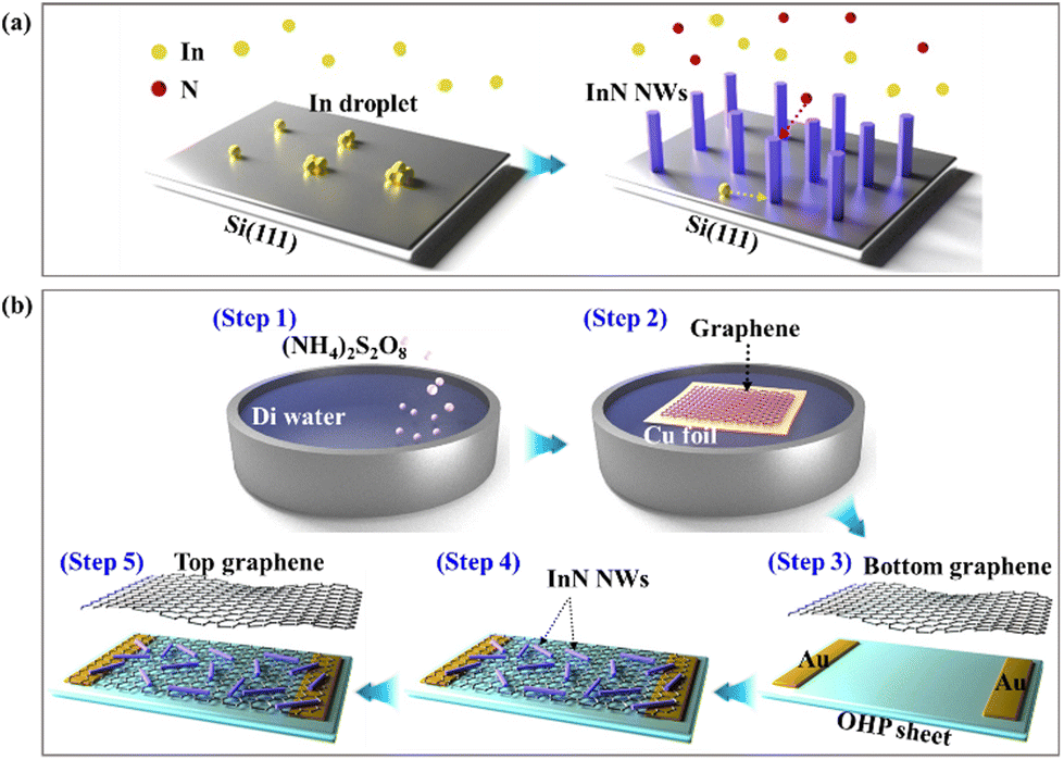 | ||
| Fig. 1 (a) Schematic illustration of the formation of InN NWs using the In pre-deposition method. (b) Fabrication process of a flexible photodetector with InN NWs and graphene. | ||
The surface morphologies of the InN NWs and fabricated flexible photodetectors were measured by field-emission scanning electron microscopy (FE-SEM, Hitachi Su-70, installed in the Future Energy Convergence Core Center at Jeonbuk National University). Double-crystal X-ray diffraction (DCXRD, Rigaku MAX-2500) and aberration-corrected (Cs) transmission electron microscopy (TEM, Jeol JEM-ARM200F) were used to analyse the structural properties of the InN NWs. Photoluminescence (PL) spectroscopy was used to investigate the optical properties of the InN NWs. PL measurements were performed using a diode-pumped solid-state laser with a wavelength of 1064 nm as an excitation source. The structural properties of graphene used as the carrier channel were investigated by Raman spectroscopy (Renishaw inVia Reflex instrument).
Results and discussion
Fig. 2a shows the cross-sectional (top) and plan-view (bottom) FE-SEM images of InN NWs formed on Si(111) substrates at the growth temperatures of 500 (NW1), 525 (NW2), 550 (NW3), and 575 °C (NW4). The surfaces of the InN NWs shown in the plan-view FE-SEM images have hexagonal shapes, which is evidence of the formation of the InN NWs with the wurtzite (WZ) crystal structure. The average lengths of NW1, NW2, NW3, and NW4 were found to be 292, 422, 524, and 545 nm, respectively. As the growth temperature increases, the average length of the InN NWs increases because the migration energy of In adatoms increases.17Fig. 2b shows the DCXRD rocking curves of the InN NW samples. The peak observed at 28.32° is attributed to the Si(111) substrate. The peak corresponding to InN(0002) is located at 31.22, 31.25, 31.30, and 31.25° for the NW1, NW2, NW3, and NW4 samples, respectively. This result indicates that the InN NWs with the [0002]-oriented WZ crystal structure were formed on Si.14,18 The full-width at half-maximum (FWHM) values of the InN(0002) peak were found to be 0.19, 0.17, 0.16, and 0.18° for the NW1, NW2, NW3, and NW4 samples, respectively. The intensity ratio, defined as the ratio of the peak intensity of InN(0002) to that of Si(111), for NW1, NW2, NW3, and NW4 was calculated to be 0.31, 1.12, 21.03, and 1.34, respectively. The NW3 sample showed the highest intensity ratio among the NW samples, indicating that it has the best crystal quality.19Fig. 2c shows the PL spectrum of the NW3 sample measured at room temperature (RT) under an excitation power of 3 mW cm−2. It is typically difficult to measure a free-exciton (FX) peak from the III-nitride thin films, nanostructures, and NWs at RT because a considerable number of defects including stacking faults are generated, especially at the interface. That is, because a significant number of photogenerated carriers inside the NWs can be trapped at defects, the radiative recombination becomes insufficient, resulting in an extremely weak FX emission.20 For the InN NWs in this study, however, the FX peak was clearly observed at the wavelength of 1.30 μm at RT, and the valley observed around 1.33 μm is related to water absorption.21 Compared to the previously reported emission wavelengths (∼1.63 μm) of InN thin films, the peak position of the InN NWs in this work is considerably blue-shifted. This result is attributed to the combined effect of the Burstein–Moss shift and the quantum size effect of the InN NWs.22,23Fig. 2d shows the Cs-TEM image of a single InN NW for the NW3 sample. The high-resolution TEM (HRTEM) images and selective-area electron diffraction (SAED) patterns measured from three different positions of the InN NW along the vertical growth direction are shown at the bottom of the TEM image. | ||
| Fig. 2 (a) Cross-sectional (top) and plan-view (bottom) FE-SEM images of the InN NWs. (Scale bars: 200 nm.) (b) DCXRD rocking curves of the InN NWs grown on Si(111) substrates. (c) PL spectrum of the InN NWs measured at RT. (d) Cs-TEM image (top), HRTEM images (bottom), and SAED patterns (inset) measured at three different vertical positions. (Scale bars of HRTEM images: 5 nm.) | ||
The HRTEM images and SAED patterns show that some stacking faults appear in the bottom region of the InN NW mainly due to the large difference in the lattice constants and the thermal expansion coefficients between the InN and Si. However, the stacking faults in the InN NWs drastically disappeared along the vertical growth direction because of the significant reduction of the lattice mismatch and the difference in the thermal expansion coefficient.24,25 The SAED patterns measured at the top, middle, and bottom regions show the growth directions of [0002] and [01−10], indicating the formation of InN NWs with the WZ crystal structure.26
Fig. 3a shows the Raman spectra of graphene with different numbers of stacked layers transferred onto the OHP sheet, in which InN NWs are not dispersed. The two strong peaks observed at 1588 and 2682 cm−1 correspond to the G and 2D peaks, respectively. The intensity ratio between the G and 2D peaks (IG/I2D) of the single-layer, double-layer, triple-layer, and quadruple-layer graphene is calculated to be 0.4, 0.5, 0.8, and 1.4, respectively. As the number of graphene layers increases, the intensity of the G peak, originating from the in-plane vibration of sp2 carbon atoms, increases because more carbon atoms are detected in multilayer graphene.27 The FWHM value of the 2D peak was calculated to be 46.4, 47.7, 61.7, and 64.5 cm−1 for the single-layer, double-layer, triple-layer, and quadruple-layer bottom graphene, respectively. The 2D peak was broadened with increasing the stacking layer of graphene, which is attributed to a hole-doping effect that occurred during the transfer process and complex double resonance from the turbostratic-stacked graphene.28–30 Typically, strain due to spatial lattice deformation during the transfer process causes an asymmetry shape of the 2D peak in the Raman spectrum of graphene.31 In the Raman spectra of this work, however, the shape of the 2D peak of graphene is symmetric. This result indicates that the multilayer graphene exhibits no degradation due to the strain and physical damage during the transfer process.32,33Fig. 3b shows the photograph of the fabricated photodetectors. Fig. 3c shows the FE-SEM image of the photodetector fabricated with InN NWs and graphene. The inset shows the optical microscopy image of the fabricated flexible photodetector. The spatial density of the InN NWs in the device was calculated to be 16.6 × 1012 cm−2. Because the ultrasonic mechanical process was performed under the same conditions for several small pieces (1 × 1 cm2) obtained from one NW sample, the spatial density of the InN NWs is almost the same for the photodetectors fabricated with different stacking layers of the bottom graphene.
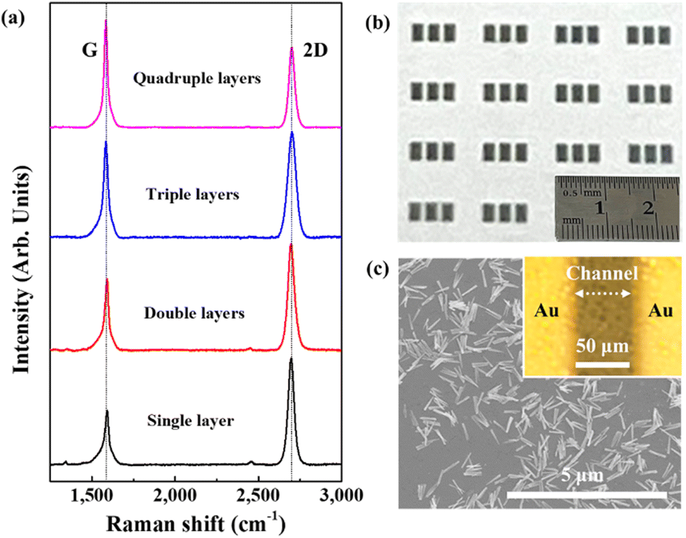 | ||
| Fig. 3 (a) Raman spectra of graphene layers transferred onto the OHP sheet. (b) Photograph of the fabricated photodetector. (c) Plan-view FE-SEM image of the InN NWs used as the absorbing medium and the optical microscopy image (inset) of the flexible photodetector. | ||
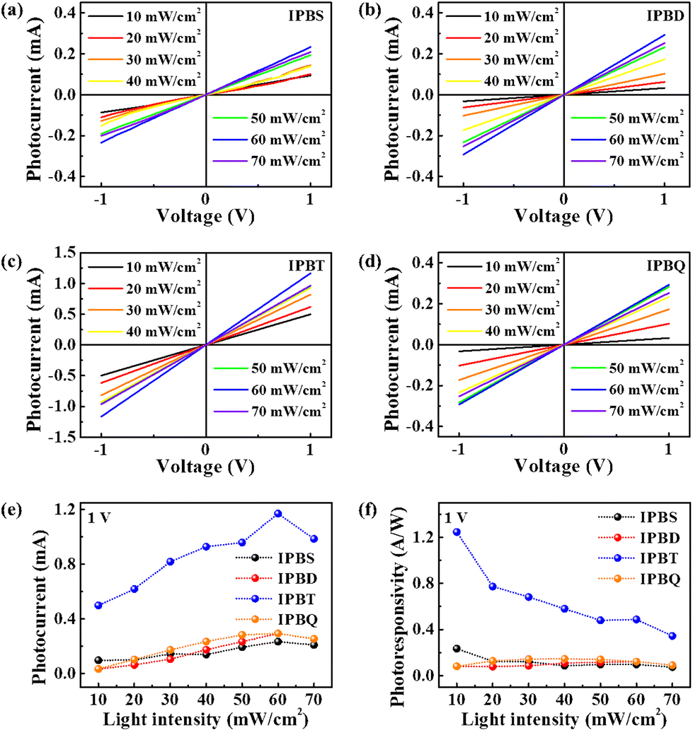
Fig. 4a–d show the current (I) versus voltage (V) characteristic curves of the flexible photodetectors with different stacking numbers of the bottom graphene layer, measured by varying the light intensity from 10 to 70 mW cm−2 of a white light (xenon lamp). The photocurrent is calculated by subtracting the dark current from the light current.9 According to previous reports, graphene cannot absorb light at the near-infrared wavelength.34,35 Therefore, the effect of the graphene channel on the absorption of light with a wavelength of 1.3 μm is negligible for our devices. At the light intensity of 60 mW cm−2 and the voltage of 1 V, the photocurrents of the IPBS, IPBD, IPBT, and IPBQ chips were found to be 0.23, 0.29, 1.17, and 0.29 mA, respectively. The photocurrent of the IPBT sample is higher than those of the IPBS and IPBD, which is related to the relatively large effective volume of the triple-layer graphene in which carriers generated in the InN NWs can migrate. Consequently, photogenerated carriers can contribute to the electrical signal more efficiently compared to those for the single-layer and double-layer graphene.36,37 However, the photocurrent of the IPBQ chip is lower than that of the IPBT sample. For single-layer, double-layer, and triple-layer graphene, the accommodation of carriers may dominate over the scattering effects of the multilayer graphene such as Coulomb scattering, short-range scattering, and surface polar phonon scattering.36 For the quadruple-layer graphene, however, the effect of the scattering interferes with the carrier movement, resulting in a decrease in the carrier movement from the InN NWs to the electrodes via the graphene channel.36 As a result, the photocurrent of the IPBT chip was the highest among the InN-NW photodetectors under the same experimental conditions. The photocurrent of our flexible device is higher than those reported in previous studies on photodetectors operating at the wavelength of 1.3 μm.38–42Fig. 4e shows the summary of the photocurrents as a function of light intensity at the voltage of 1 V. As the light intensity increases from 10 to 60 mW cm−2, the number of photogenerated carriers contributing to the photocurrent increases, resulting in the increase in the photocurrent. However, when the light intensity increases to 70 mW cm−2, the photocurrent slightly decreases due to electron–phonon scattering.43Fig. 4f shows the photoresponsivity measured at the various light intensities and the voltage of 1 V. The photoresponsivities of the IPBS, IPBD, IPBT, and IPBQ were calculated to be 0.23, 0.08, 1.25, and 0.08 A W−1, respectively, at the light intensity of 10 mW cm−2. The photoresponsivity of the IPBT sample is higher than those of the other devices. Since the photoresponsivity of the photodetector is derived from the photocurrent, the difference in the photoresponsivities depending on the number of bottom graphene layers can be also interpreted in the same way as described in the photocurrent result. The photoresponsivity of the IPBT chip is higher than those of previously reported infrared photodetectors.41,42,44–47 The improvement of the photocurrent and photoresponsivity of the flexible photodetector is attributed to the efficient generation of carriers at the light-absorbing media because InN NWs have high crystallinity. The InN NWs embedded in the graphene sandwich structure cause spatially unintentional uneven surfaces. According to the previous works on the flexible and stretchable photosensors fabricated with GaN NWs and graphene, the effect of uneven surfaces on the device performance could be neglected due to the conformal contact.10,48 That is, the conformal contact, in which the top graphene layer wraps the surface of the InN NWs, minimizes unintentional scattering and recombination of photogenerated carriers at the interface between the NWs and graphene. Consequently, the photogenerated carriers in the InN NWs can migrate into the graphene channel without significant loss.49 In addition, because graphene has high carrier mobility, the loss via the recapture of carriers in the InN NWs may be extremely small during their migration toward Au electrodes through the graphene channel. As a result, most of the carriers can effectively contribute to the photocurrent of the photodetector.50 Because of the conformal contact and high electron mobility of the graphene channel, the alignment of the InN NWs also rarely affects the device performance.10,48 That is, the generation rate of carriers by light absorption at the InN NWs dominantly influences the device performance.
 | ||
| Fig. 4 I–V characteristic curves of the flexible photodetectors depending on the number of bottom graphene layers: (a) IPBS, (b) IPBD, (c) IPBT, and (d) IPBQ. Summary of the (e) photocurrent and (f) photoresponsivity of the flexible photodetectors depending on the light intensity at the voltage of 1 V. | ||
To investigate the effect of the volume of the light-absorbing medium on the device performance, flexible photodetectors with lengths of 292 (IPNW1), 422 (IPNW2), 524 (IPNW3), and 545 nm (IPNW4) were also fabricated, in which the triple-layer graphene was used for the bottom channel. The IPNW3 is the same as the IPBT. Fig. 5a and b show the I–V characteristic curves and summary of photocurrent and photoresponsivity of the flexible photodetectors with different lengths of the InN NWs, measured at the voltage of 1 V and the light intensity of 60 mW cm−2, respectively. The photocurrent and photoresponsivity of the IPNW3 are higher than those of the IPNW1 and IPNW2. This result is largely attributed to the increase in the effective volume of the light-absorbing medium with increasing the length of the InN NWs.9 The device performance of the IPNW4 is almost the same as that of the IPNW3, because the difference in the length of the NWs is small.
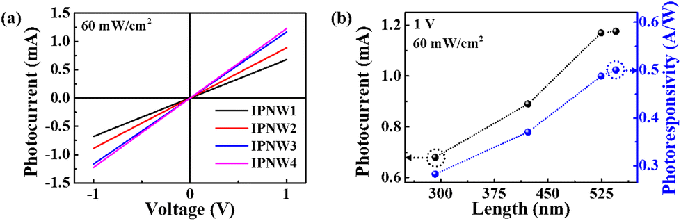 | ||
| Fig. 5 (a) I–V characteristic curves and (b) summary of the photocurrent and photoresponsivity of the flexible photodetectors with respect to the length of the InN NWs. | ||
Fig. 6a and b show the schematic and the energy-band structure to explain the operation mechanism of the flexible photodetector, respectively. At the hetero-interface between the InN NWs and graphene as shown in Fig. 6b, the difference between the electron affinity of the InN NW and the work function of graphene causes the downward energy-band bending of the InN-NW surface to match the Fermi level. As a result, electrons generated by light absorption in the InN NWs can migrate easily to the graphene channel and contribute to the photocurrent.
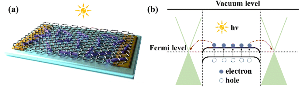 | ||
| Fig. 6 (a) Schematic diagram of a photodetector and (b) transfer process of carriers from InN NWs to the graphene channel. | ||
To evaluate the flexibility of the photodetectors, their photocurrent and photoresponsivity were measured with respect to the degree of strain controlled by the bending radius of the IPBT chip and are shown in Fig. 7a. The light intensity and the voltage for the measurements were 60 mW cm−2 and 1 V, respectively. Bending radii of 9.3, 4.6, and 3.1 mm correspond to the strain of 1, 2, and 3%, respectively. As shown in Fig. 7a, the device parameters are degraded with increasing the degree of strain, but the change is small enough to neglect. The photocurrent (photoresponsivity) of the IPBT chip was found to be 1.15 mA (1.24 A W−1) under the strain condition of 3% (bending radius = 3.1 mm), which corresponds to 98.3% (99.2%) compared to the value obtained before bending. Cyclic-bending tests of the IPBT chip were performed at the bending radius of 3.1 mm. The speed of the bending machine applying the strain to the flexible photodetector was set to 10.5 mm s−1. Fig. 7b shows the photocurrent and photoresponsivity of the IPBT sample measured after the cyclic-bending tests. The photocurrent and photoresponsivity of the flexible photodetector slightly decrease with increasing bending cycles. The photocurrent and photoresponsivity of the IPBT chip measured after the 200 cyclic-bending tests are comparable to the values obtained before bending. This result indicates that the fabricated flexible photodetector has reliable mechanical stability. Thus, we successfully fabricated flexible 1.3 μm photodetectors applicable to wearable or attachable systems for wireless optical communication.
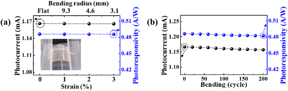 | ||
| Fig. 7 Photocurrent and photoresponsivity of the photodetectors under bending tests with respect to (a) bending radius and (b) bending cycles. The inset shows the image of a flexible photodetector under bending. | ||
Conclusions
In summary, we successfully fabricated flexible photodetectors, operating at the wavelength window of 1.3 μm, using InN NWs and graphene on an OHP sheet. The InN NWs with high-crystal quality and uniformity were successfully grown on Si(111) using the In pre-deposition method. The photocurrent of the flexible photodetector was found to be 1.17 mA at the light intensity of 60 mW cm−2. At the light intensity of 10 mW cm−2, the photoresponsivity was found to be 1.25 A W−1. These results indicate that the flexible photodetectors fabricated with InN NWs and graphene show better performances compared to those of the previous reports. The improvement of the device performance is attributed to the high crystallinity of the InN NWs used as a light-absorbing medium, a conformal contact between the InN NWs and graphene, and fast carrier mobility of graphene. After the bending tests, the photocurrent and photoresponsivity of the flexible photodetector are comparable to those measured before bending. This result indicates that the fabricated flexible photodetectors have high mechanical stability.Author contributions
J. S. K. designed the research project and supervised the experiments. J. S., H. Y., S. N., and S. H. performed the experiments and analysed the data. J. S. K. and J. S. wrote the paper, which was discussed by all the authors.Conflicts of interest
There are no conflicts to declare.Acknowledgements
This work was supported by the National Research Foundation of Korea (NRF) funded by the Ministry of Education (2018R1D1A1B07043442).Notes and references
- D. Khandal and S. Jain, Li-Fi (Light Fidelity): The future technology in wireless communication, Int. J. Inf. Comput. Technol., 2014, 4, 1687–1694 Search PubMed.
- R. Karthika and S. Balakrishnan, Wireless communication using Li-Fi technology, SSRG Int. J. Electron. Commun. Eng., 2015, 2, 32–40 Search PubMed.
- C. Medina, M. Zambrano and K. Navarro, LED based visible light communication: technology, application and challenges–a survey, Signals Commun. Technol., 2015, 8, 482 Search PubMed.
- P. K. Sharma, J. H. Ryu, K. Y. Park, J. H. Park and J. H. Park, Li-Fi based on security cloud framework for future IT environment, Hum. Cent. Comput. Inf. Sci., 2018, 8, 1–13 CrossRef.
- N. Guan, X. Dai, A. V. Babichev, F. H. Julien and M. Tchernycheva, Flexible inorganic light emitting diodes based on semiconductor nanowires, Chem. Sci., 2017, 8, 7904–7911 RSC.
- H. Kum, D. Lee, W. Kong, H. Kim, Y. Park, Y. Kim, Y. Baek, S.-H. Bae, K. Lee and J. Kim, Epitaxial growth and layer-transfer techniques for heterogeneous integration of materials for electronic and photonics devices, Nat. Electron., 2019, 2, 439–450 CrossRef CAS.
- M. Peng, Y. Liu, A. Yu, Y. Zhang, C. Liu, J. Liu, W. Wu, K. Zhang, X. Shi, J. Kou, J. Zhai and Z. L. Wang, Flexible self-powered GaN ultraviolet photoswitch and piezo-phototronic effect enhanced on/off ratio, ACS Nano, 2016, 10, 1572–1579 CrossRef CAS PubMed.
- S. Weiszer, A. Zeidler, M. D. L. Mata and M. Stutzmann, Growth of self-assembled and position-controlled InN nanowires on Si(111) by molecular beam epitaxy, J. Cryst. Growth, 2019, 510, 56–64 CrossRef CAS.
- S. Han, S.-K. Lee, I. Choi, J. Song, C.-R. Lee, K. Kim, M.-Y. Ryu, K.-U. Jeong and J. S. Kim, Highly efficient and flexible photosensors with GaN nanowires horizontally embedded in a graphene sandwich channel, ACS Appl. Mater. Interfaces, 2018, 10, 38173–38182 CrossRef CAS PubMed.
- S. Han, S. Noh, J.-W. Kim, C.-R. Lee, S.-K. Lee and J. S. Kim, Stretchable inorganic GaN-nanowire photosensor with high photocurrent and photoresponsivity, ACS Appl. Mater. Interfaces, 2021, 13, 22728–22737 CrossRef CAS PubMed.
- D. W. Park, S. G. Jeon, C.-R. Lee, S. J. Lee, J. Y. Song, J. O. Kim, S. K. Noh, J.-Y. Leem and J. S. Kim, Structural and electrical properties of catalyst-free Si-doped InAs nanowires formed on Si (111), Sci. Rep., 2015, 5, 1–8 Search PubMed.
- V. Parameshwaran, X. Xu and B. Clemens, Crystallinity, surface morphology, and photoelectrochemical effects in conical InP and InN nanowires grown on silicon, ACS Appl. Mater. Interfaces, 2016, 8, 21454–21464 CrossRef CAS PubMed.
- M. H. Kim, D. Y. Moon, J. Park, Y. Nanishi, G.-C. Yi and E. Yoon, Catalyst–free growth of InN nanorods by metal–organic chemical vapor deposition, Phys. Status Solidi A, 2012, 209, 50–55 CrossRef CAS.
- S. Noh, S. Han, J. Shin, J. Lee, I. Choi, H. M. Oh, M.-Y. Ryu and J. S. Kim, Photoelectrochemical water splitting using GaN nanowires with reverse-mesa structures as photoanode material, Appl. Sci. Converg. Technol., 2022, 31, 51–55 CrossRef.
- S. Bae, H. Kim, Y. Lee, X. Xu, J.-S. Park, Y. Zheng, J. Balakrishnan, T. Lei, H. R. Kim, Y. I. Song, Y.-J. Kim, K. S. Kim, B. Özyilmaz, J.-H. Ahn, B. H. Hong and S. Iijima, Roll-to-roll production of 30-inch graphene films for transparent electrodes, Nat. Nanotechnol., 2010, 5, 574–578 CrossRef CAS PubMed.
- S. Han, I. Choi, K. Lee, C.-R. Lee, S.-K. Lee, J. Hwang, D. G. Chung and J. S. Kim, Dependence of internal crystal structures of InAs nanowires on electrical characteristics of field effect transistors, J. Electron. Mater., 2018, 47, 944–948 CrossRef CAS.
- S. Han, I. Choi, J. Song, C.-R. Lee, I.-W. Cho, M.-Y. Ryu and J. S. Kim, Structural and optical properties of GaN nanowires formed on Si(111), Appl. Sci. Converg. Technol., 2018, 27, 95–99 CrossRef.
- S. Feng, J. Tan, B. Li, H. Song, Z. Wu and X. Chen, Nitridation effects of Si (111) substrate surface on InN nanorods grown by plasma-assisted molecular beam epitaxy, J. Alloys Compd., 2015, 621, 232–237 CrossRef CAS.
- P. Sangeetha, K. Jeganathan and V. Ramakrishnan, Micro-Raman investigations of InN-GaN core-shell nanowires on Si(111) substrate, AIP Adv., 2013, 3, 062114 CrossRef.
- T. Auzelle, B. Haas, M. D. Hertog, J.-L. Rouvière, B. Daudin and B. Gayral, Attribution of the 3.45 eV GaN nanowires luminescence to inversion domain boundaries, Appl. Phys. Lett., 2015, 107, 051904 CrossRef.
- E. Thimsen, B. Sadtler and M. Y. Berezin, Shortwave-infrared (SWIR) emitters for biological imaging: a review of challenges and opportunities, Nanophotonics, 2017, 6, 1043–1054 CAS.
- K. K. Madapu and S. Dhara, Effect of strain relaxation and the Burstein–Moss energy shift on the optical properties of InN films grown in the self-seeded catalytic process, CrystEngComm, 2016, 18, 3114–3123 RSC.
- W. C. Ke, C. P. Fu, C. Y. Chen, L. Lee, C. S. Ku, W. C. Chou, W.-H. Chang, M. C. Lee and W. K. Chen, Photoluminescence properties of self-assembled InN dots embedded in GaN grown by metal organic vapor phase epitaxy, Appl. Phys. Lett., 2006, 88, 191913 CrossRef.
- T. R. Kuykendall, M. V. P. Altoe, D. F. Ogletree and S. Aloni, Catalyst-directed crystallographic orientation control of GaN nanowire growth, Nano Lett., 2014, 14, 6767–6773 CrossRef CAS PubMed.
- K. Tomioka, J. Motohisa, S. Hara and T. Fukui, Control of InAs nanowire growth directions on Si, Nano Lett., 2008, 8, 3475–3480 CrossRef CAS PubMed.
- H. J. Joyce, J. Wong-Leung, Q. Gao, H. H. Tan and C. Jagadish, Phase perfection in zinc blende and wurtzite III–V nanowires using basic growth parameters, Nano Lett., 2010, 10, 908–915 CrossRef CAS PubMed.
- Z. Ni, Y. Wang, T. Yu and Z. Shen, Raman spectroscopy and imaging of graphene, Nano Res., 2008, 1, 273–291 CrossRef CAS.
- H.-Y. Kim, O. M. Dawood, U. Monteverde, J. Sexton, Z. Li, L. Britnell, M. A. Migliorato, R. J. Young and M. Missous, Multilayer stacking and metal deposition effects on large area graphene on GaAs, Carbon, 2016, 96, 83–90 CrossRef CAS.
- Z. Wang, H. Ogata, S. Morimoto, M. Fujishige, K. Takeuchi, H. Muramatsu, T. Hayashi, J. Ortiz-Medina, M. Z. M. Yusop, M. Tanemura, M. Terrones, Y. Hashimoto and M. Endo, Microwave plasma-induced graphene-sheet fibers from waste coffee grounds, J. Mater. Chem. A, 2015, 3, 14545–14549 RSC.
- A. H. Alami, K. Aokal, D. Zhang and B. Soudan, Bulk turbostratic graphene deposition on aluminum substrates via high-pressure graphite blasting, Appl. Nanosci., 2018, 8, 1943–1950 CrossRef CAS.
- C. Neumann, S. Reichardt, P. Venezuela, M. Drögeler, L. Banszerus, M. Schmitz, K. Watanabe, T. Taniguchi, F. Mauri, B. Beschoten, S. V. Rotkin and C. Stampfer, Raman spectroscopy as probe of nanometre-scale strain variations in graphene, Nat. Commun., 2015, 6, 1–7 Search PubMed.
- R. Beams, L. G. Cançado and L. Novotny, Raman characterization of defects and dopants in graphene, J. Phys.: Condens. Matter, 2015, 27, 083002 CrossRef CAS PubMed.
- X.-L. Li, X.-F. Qiao, W.-P. Han, Y. Lu, Q.-H. Tan, X.-L. Liu and P.-H. Tan, Layer number identification of intrinsic and defective multilayered graphenes up to 100 layers by the Raman mode intensity from substrates, Nanoscale, 2015, 7, 8135–8141 RSC.
- A. Kumar, G. Sachdeve, R. Pandey and S. P. Karna, Optical absorbance in multilayer two-dimensional materials: Graphene and antimonene, Appl. Phys. Lett., 2020, 116, 263102 CrossRef CAS.
- Y. Cai, J. Zhu and Q. H. Liu, Tunable enhanced optical absorption of graphene using plasmonic perfect absorbers, Appl. Phys. Lett., 2015, 106, 043105 CrossRef.
- W. Zhu, V. Perebeinos, M. Freitag and P. Avouris, Carrier scattering, mobilities, and electrostatic potential in monolayer, bilayer, and trilayer graphene, Phys. Rev. B: Condens. Matter Mater. Phys., 2009, 80, 235402 CrossRef.
- J. Ye, M. F. Craciun, M. Koshino and Y. Iwasa, Accessing the transport properties of graphene and its multilayers at high carrier density, Proc. Natl. Acad. Sci. U. S. A., 2011, 108, 13002–13006 CrossRef CAS PubMed.
- F.-X. Liang, X.-Y. Zhao, J.-J. Jiang, J.-G. Hu, W.-Q. Xie, J. Lv, Z.-X. Zhang, D. Wu and L.-B. Luo, Light confinement effect induced highly sensitive, self-driven near-infrared photodetector and image sensor based on multilayer PdSe2/pyramid Si heterojunction, Small, 2019, 15, 1903831 CrossRef CAS PubMed.
- M. A. Nazirzadeh, F. B. Atar, B. B. Turgut and A. K. Okyay, Random sized plasmonic nanoantennas on silicon for low-cost broad-band near-infrared photodetection, Sci. Rep., 2014, 4, 1–5 Search PubMed.
- L. Ma, X. Zhang, H. Li, H. Tan, Y. Yang, Y. Xu, W. Hu, X. Zhu, X. Zhuang and A. Pan, Bandgap-engineered GaAsSb alloy nanowires for near-infrared photodetection at 1.31 μm, Semicond. Sci. Technol., 2015, 30, 105033 CrossRef.
- P. Ma, N. Flöry, Y. Salamin, B. Baeuerle, A. Emboras, A. Josten, T. Taniguchi, K. Watanabe, L. Novotny and J. Leuthold, Fast MoTe2 waveguide photodetector with high sensitivity at telecommunication wavelengths, ACS Photonics, 2018, 5, 1846–1852 CrossRef CAS.
- C.-L. Hsin, S.-M. Wang, G.-Y. Chen, M.-S. Wu, C.-W. Huang, S.-C. Hsu and S.-C. Lo, Si/Ge/Si photodetector by rapid-melting-growth technique, IEEE Trans. Nanotechnol., 2018, 17, 607–610 CAS.
- J. H. Seol, I. Jo, A. L. Moore, L. Lindsay, Z. H. Aitken, M. T. Pettes, X. Li, Z. Yao, R. Huang, D. Broido, N. Mingo, R. S. Ruoff and L. Shi, Two-dimensional phonon transport in supported graphene, Science, 2010, 328, 213–216 CrossRef CAS PubMed.
- L. Zhou, Y. G. Zhang, X. Y. Chen, Y. Gu, H. S. B. Y. Li, Y. Y. Cao and S. P. Xi, Dark current characteristics of GaAs-based 2.6 μm InGaAs photodetectors on different types of InAlAs buffer layers, J. Phys. D: Appl. Phys., 2014, 47, 085107 CrossRef CAS.
- P. Wang, S. Liu, W. Luo, H. Fang, F. Gong, N. Guo, Z.-G. Chen, J. Zou, Y. Huang, X. Zhou, J. Wang, X. Chen, W. Lu, F. Xiu and W. Hu, Arrayed van der Waals broadband detectors for dual–band detection, Adv. Mater., 2017, 29, 1604439 CrossRef PubMed.
- J. Ge, M. Luo, W. Zou, W. Peng and H. Duan, Plasmonic photodetectors based on asymmetric nanogap electrodes, Appl. Phys. Express, 2016, 9, 084101 CrossRef.
- H. Liu, X. Zhu, X. Sun, C. Zhu, W. Huang, X. Zhang, B. Zheng, Z. Zou, Z. Luo, X. Wang, D. Li and A. Pan, Self-powered broad-band photodetectors based on vertically stacked WSe2/Bi2Te3 p-n heterojunctions, ACS Nano, 2019, 13, 13573–13580 CrossRef CAS PubMed.
- S. Han, I. Choi, C.-R. Lee, K.-U. Jeong, S.-K. Lee and J. S. Kim, Fast response characteristics of flexible ultraviolet photosensors with GaN nanowires and graphene, ACS Appl. Mater. Interfaces, 2019, 12, 970–979 CrossRef PubMed.
- W. Jung, D. Kim, M. Lee, S. Kim, J.-H. Kim and C.-S. Han, Ultraconformal contact transfer of monolayer graphene on metal to various substrates, Adv. Mater., 2014, 26, 6394–6400 CrossRef CAS PubMed.
- K. Lee, C.-R. Lee, T.-H. Chung, J. Park, J.-Y. Leem, K.-U. Jeong and J. S. Kim, Influences of graded superlattice on the electrostatic discharge characteristics of green InGaN/GaN light-emitting diodes, J. Cryst. Growth, 2017, 464, 138–142 CrossRef CAS.
| This journal is © The Royal Society of Chemistry 2022 |