
 Open Access Article
 This Open Access Article is licensed under a Creative Commons Attribution-Non Commercial 3.0 Unported Licence
Tailoring ZnO nanowire crystallinity and morphology for label-free capturing of extracellular vesicles†
Piyawan
Paisrisarn
 a,
Takao
Yasui
*abc,
Zetao
Zhu
ac,
Annop
Klamchuen
d,
Panita
Kasamechonchung
d,
Tuksadon
Wutikhun
d,
Visittapong
Yordsri
e and
Yoshinobu
Baba
acf
a,
Takao
Yasui
*abc,
Zetao
Zhu
ac,
Annop
Klamchuen
d,
Panita
Kasamechonchung
d,
Tuksadon
Wutikhun
d,
Visittapong
Yordsri
e and
Yoshinobu
Baba
acf
aDepartment of Biomolecular Engineering, Graduate School of Engineering, Nagoya University, Furo-cho, Chikusa-ku, Nagoya 464-8603, Japan. E-mail: yasui@chembio.nagoya-u.ac.jp
bJapan Science and Technology Agency (JST), PRESTO, 4-1-8 Honcho, Kawaguchi, Saitama 332-0012, Japan
cInstitute of Nano-Life-Systems, Institutes of Innovation for Future Society, Nagoya University, Furo-cho, Chikusa-ku, Nagoya 464-8603, Japan
dNational Nanotechnology Center (NANOTEC), National Science and Technology Development Agency (NSTDA), Pathum Thani 12120, Thailand
eNational Metal and Materials Technology Center (MTEC), National Science and Technology Development Agency (NSTDA), Pathum Thani 12120, Thailand
fInstitute of Quantum Life Science, National Institutes for Quantum and Radiological Science and Technology, Anagawa 4-9-1, Inage-ku, Chiba 263-8555, Japan
First published on 2nd March 2022
Abstract
Zinc oxide (ZnO) nanowires have shown their potential in isolation of cancer-related biomolecules such as extracellular vesicles (EVs), RNAs, and DNAs for early diagnosis and therapeutic development of diseases. Since the function of inorganic nanowires changes depending on their morphology, previous studies have established strategies to control the morphology and have demonstrated attainment of improved properties for gas and organic compound detection, and for dye-sensitized solar cells and photoelectric conversion performance. Nevertheless, crystallinity and morphology of ZnO nanowires for capturing EVs, an important biomarker of cancer, have not yet been discussed. Here, we fabricated ZnO nanowires with different crystallinities and morphologies using an ammonia-assisted hydrothermal method, and we comprehensively analyzed the crystalline nature and oriented growth of the synthesized nanowires by X-ray diffraction and selected area electron diffraction using high resolution transmission electron microscopy. In evaluating the performance of label-free EV capture in a microfluidic device platform, we found both the crystallinity and morphology of ZnO nanowires affected EV capture efficiency. In particular, the zinc blende phase was identified as important for crystallinity, while increasing the nanowire density in the array was important for morphology to improve EV capture performance. These results highlighted that the key physicochemical properties of the ZnO nanowires were related to the EV capture performance.
 Takao Yasui | Takao Yasui is an Associate Professor of Department of Biomolecular Engineering, Graduate School of Engineering at Nagoya University, a PRESTO Researcher at the Japan Science and Technology Agency (JST), and a co-founder and a Nanodevice Director at Craif Inc. In 2011, he received his PhD in the Department of Applied Chemistry, Graduate School of Engineering from Nagoya University. He has received over 35 awards for his contributions in the field of oxide nanowire microfluidics. His research interests are focused on designing, fabricating, and characterizing oxide nanowire microfluidics for applications in healthcare, diagnosis, sensing biomolecules and engineering biology. |
Introduction
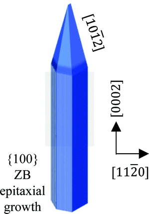
At the nanoscale, device properties and performance are no longer dependent solely on the material type, but also on material geometry. Nanowires, anisotropic structures with diameters from one to hundreds of nanometers and lengths of tens to hundreds of microns, provide a unique platform for harnessing nanoscale phenomena.1 Semiconductor nanowires are a broad class of materials which, through controlled growth and organization, have led to a number of novel nanoscale mechanical, electrochemical, thermoelectric, photonic and electronic devices.2–4 In order to produce and utilize these properties for nanowires, reliable and controllable nanowire syntheses are required. A hydrothermal method offers flexible control over nanowire crystal structure and growth orientation, enabling fabrication of high-quality single-crystalline materials with control of diameter, length, composition, and phase.5 When ZnO nanowires are hydrothermally synthesized, they are single crystals, and as a result of their narrow diameter, the nanowires have an extremely high surface area allowing highly sensitive interaction with various substances.6–9 This high surface-to-volume ratio makes the nanowires very sensitive to changes in surface chemistry and permits rapid interaction with comparatively small sizes of biomolecules including extracellular vesicles (EVs) and nucleic acids giving rise to their prevalence in isolation and detection technology development.10–15The physical phenomena in the radial and axial directions and the high surface-to-volume ratios of the nanowires have been controlled and that has led to an explosion of applications utilizing these structures. Getting preferential nucleation at the ZnO (0001) polar plane and suppressing the lateral growth, such as of the (1010) plane, are key essentials to produce a well-defined nanowire structure.16–18 Many growth parameters have been explored to manipulate the morphology of hydrothermally synthesized ZnO nanowires including the addition of auxiliary agents such as organic ligands, metal ion impurities and ammonia ions.19–24 The solution-grown ZnO nanowires generally adopt the wurtzite crystal structure and grow along the c axis with a (0002) top facet and (1010) side facets. At pH = 11 basic conditions, it was found that the top facet is negatively charge and the side facets are positively charged, enabling control of the nanowire dimensions based on the facet-selective electrostatic interaction;25 and therefore, the radial growth of colloidal nanowires can be effectively suppressed. In other words, control of the nanowire mean length and diameter can be achieved by optimizing the concentration of ammonia ions, for example. Several studies have investigated physicochemical properties of the developed high aspect ratio ZnO nanowires in various applications including photocatalysis, a piezoelectric transducer, a UV detector, photovoltaic devices, and gas and chemical sensors.26–31 To the best of our knowledge, the correlation of ZnO nanowires in terms of crystal structure and morphology with biomolecule capture has not been discussed until now.
Here, we propose a methodology using oxide nanowires with different crystallinities and morphologies synthesized by ammonia-assisted hydrothermal growth to evaluate capture performance of extracellular vesicles (EVs) and we investigate a correlation between surface crystallinity and numbers of the captured EVs. The EVs are nano- to micro-sized vesicles secreted from all cells, including cancer cells, and they are released into their environment to act as intercellular messengers.32–34 Since they enclose components from the parent cells, including nucleic acids and proteins, EVs are being examined as sources of biomarkers in various diseases, including neurodegenerative diseases, cardiovascular diseases and cancers.35–38 EVs are also being explored for the delivery of therapeutic payloads to specific cells or tissues in cancer therapeutics,39,40 owing to their distinct biological features. Cancer cell-derived EVs have the same membrane orientation as the cells: they are exposed at their surfaces to lipids and organotropic metastasis-induced transmembrane proteins.41 The enrichment of these proteoglycans has led to the idea that EVs are charged molecules.42,43 We have initiated studies exploiting ZnO nanowire integrated microfluidic devices for label-free capture of EVs through surface charge-based capture which can collect massive numbers of EVs and their molecular cargos.10,14 However, comprehensive studies of nanowires with a diverse crystal structure and morphology system have not been made yet.
Experimental
Synthesis of ZnO nanowires
We fabricated ZnO nanowires on Si substrates via a seed-assisted hydrothermal process. First, double-microchannel patterns (20 × 2 mm2) were formed by photolithography onto each silicon (100) substrate and a 20 nm thick seed layer was deposited with an electron cyclotron resonance (ECR) sputtering system (Elionix, EIS-200ERT-YN). High melting-point Cr-based alloy with purity of 99.999% was used as a sputtering target. The substrates with seed layer were oxidized in an oven at 400 °C for 2 h to prepare them as a scaffold for the ZnO nanowires. After seed layer preparation, the growth solutions were prepared using 15 mM hexamethylenetetramine (HMTA) and 15 mM zinc nitrate hexahydrate (Zn(NO3)2·6H2O) as the precursors, and 0.8 M ammonium solution was added for ultra-lengthening of ZnO nanowires. The nanowires were grown at 95 °C with varying duration times (3 h, 6 h and 9 h). We renewed the growth solutions every 3 h to maintain the concentrations.Fabrication of the microfluidic device
The dried nanowires grown on the substrate were treated with oxygen plasma. A sheet of 30 μm-depth polydimethylsiloxane (PDMS) was attached to the substrate. The sheet was patterned with two microchannels (20 × 2 mm2) and 0.05 mm inlet and outlet holes at the end of channels for sample injection.Characterization of ZnO nanowires
The morphology and the composition of ZnO nanowires were characterized with a field emission scanning electron microscope (FESEM; Carl Zeiss, Supra 40VP), a high-resolution transmission electron microscope (HRTEM; JEOL, JEM-2100) and an energy dispersive X-ray spectroscopy (EDS) system (Oxford Instruments, Ultim Max 100). For the cross-sectional SEM-EDS analysis and the single-nanowire HRTEM analysis, we utilized an accelerating voltage of 15 kV and 200 kV, respectively. The EDS mapping images were integrated for 100 cycles. The peaks of Zn Kα (8.6313 keV), O Kα (0.5249 keV), Si Kα (1.7398 keV), and Cr Kα (5.4117 keV) and were chosen to construct the elemental mapping images. An X-ray diffraction (XRD) analyzer (Bruker, D8 Advance) was used to examine the crystalline nature and oriented growth of synthesized ZnO nanowires. The conditions were set to be Cu Kα XRD source, λ = 0.1542 nm, accelerating voltage of 40 kV, acceleration current 40 mA, scan step 0.02°, scan rate 0.5 s per step, and scan range 20 to 80°. The XRD patterns were analyzed using Diffrac.EVA 5.0.Cell culture and extraction of EV by ultracentrifugation
We cultured human breast adenocarcinoma cells (MDA-MB-231) in DMEM supplemented with 10% exosome-depleted FBS and 1% penicillin streptomycin. 2 × 10⁶ cells were seeded into 15 mL of complete medium in a 75 cm2 culturing flask and incubated at 37 °C and with 5% CO2. After 48 h, the cell medium was taken from the culturing flask and filtered through a 0.22 μm filter to remove cellular debris. Next, the filtered medium was ultracentrifuged at 110![[thin space (1/6-em)]](https://www.rsc.org/images/entities/char_2009.gif) 000g, 4 °C, 80 min. After discarding the supernatant, we added 5 mL of 0.22 μm filtered PBS to wash the EV pellets, and this solution was ultracentrifuged again with the same conditions. After discarding the supernatant, 1 mL of 0.22 μm filtered PBS was added to collect EVs. The EV suspension was stored at 4 °C until use.
000g, 4 °C, 80 min. After discarding the supernatant, we added 5 mL of 0.22 μm filtered PBS to wash the EV pellets, and this solution was ultracentrifuged again with the same conditions. After discarding the supernatant, 1 mL of 0.22 μm filtered PBS was added to collect EVs. The EV suspension was stored at 4 °C until use.
Evaluation of EV capture efficiency
We integrated a nanowire device with a dual-channel syringe pump to continuously infuse EV sample with the flow rate of 10 μL min−1. 250 μL of EV-suspended PBS was supplied to the nanowire device to isolate EVs onto each nanowire. EV concentration and size were analysed using a nanoparticle tracking analysis system (Malvern Panalytical, NanoSight LM10). After appropriate dilutions, video data were collected 5 times for a 60 s time period for each video. Camera level and detection threshold were set to 13 and 5, respectively. Data analysis was performed automatically by NanoSight NTA 3.2 software. To observe EVs on nanowire surfaces, the device was left to dry naturally at room temperature. The PDMS sheet was removed from the substrate, the captured EVs on the nanowire surfaces were directly observed using FESEM at 5 kV of accelerating voltage without any fixing or coating processes.Results and discussion
For controlling the morphology of ZnO nanowires, we introduced ammonia solution into the ZnO precursor growth solution during the growth step and hydrothermally fabricated nanowires in varying growth duration times for 3, 6, and 9 h. Ammonium hydroxide is an additive that has been widely used to enhance the nanowire growth rate along the c-axial ZnO plane via face-selective electrostatic crystal growth inhibition.25 As ammonia concentration was reported to critically affect the morphology of nanowires,26,44,45 we evaluated the optimum concentration of ammonia for our experimental conditions and found the concentration of ammonia at 0.8 M provided the longest nanowires (Fig. S1†). The pH values in growth solutions with ammonia addition (Fig. S2†) indicated the presence of OH− ions during the time before nanowire growth (initial) to after it (final). Morphology observations showed that the nanowires obtained were larger in length and diameter in comparison to nanowires grown without ammonia addition, and nanowire length could be enlarged by increasing the growth duration time (Fig. 1a and b). The EDS mapping images of Zn Kα as a main constituent of the synthesized nanowires confirmed that various lengths of ZnO nanowires could be obtained by using the ammonia-assisted hydrothermal fabrication method (Fig. 1c and Fig. S3†).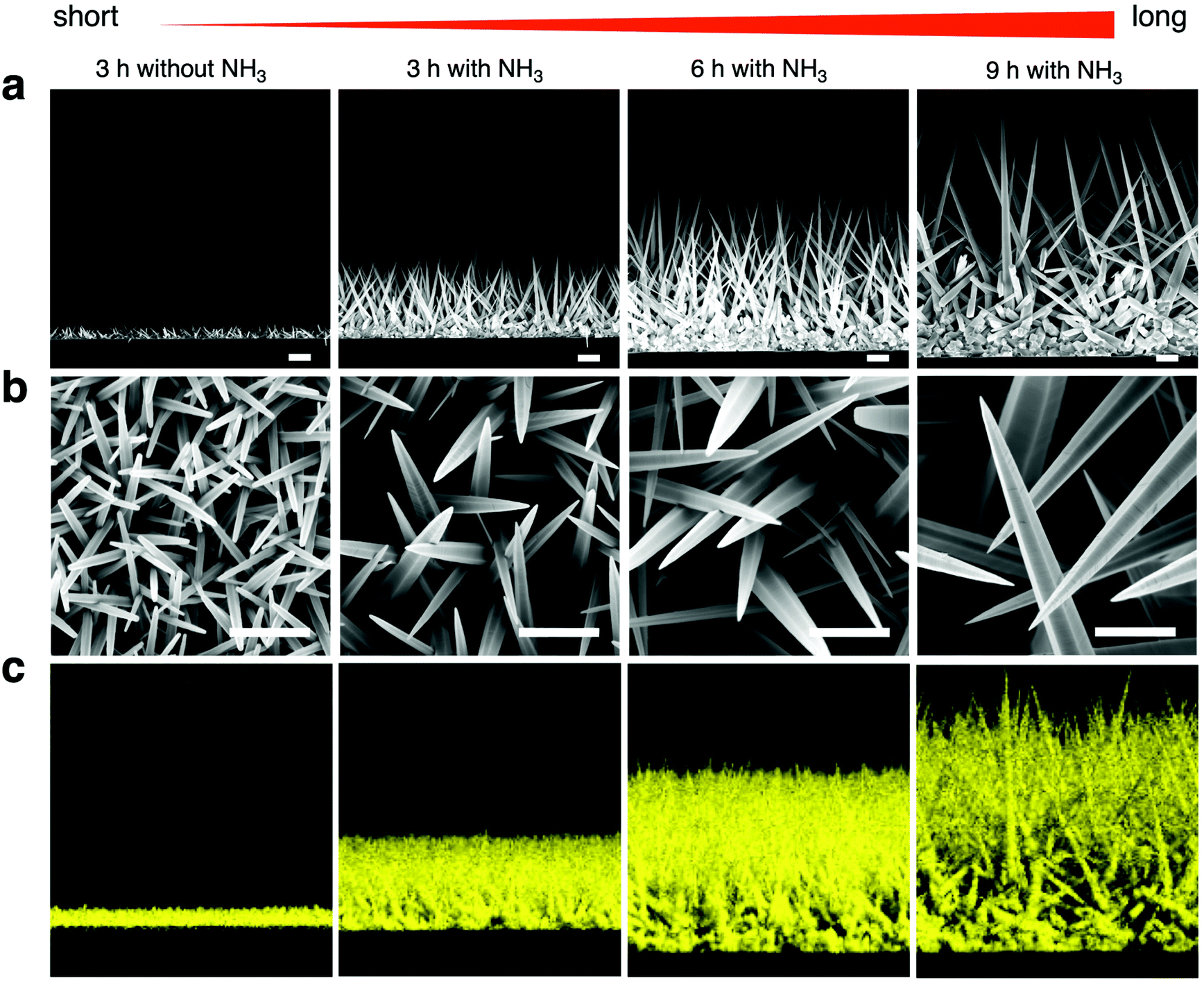 | ||
| Fig. 1 (a) FESEM images of cross-sectional nanowires for different growth conditions. The scale bars are 2 μm. (b) FESEM images of top-view nanowires. The scale bars are 1 μm. (c) Elemental mapping of Zn Kα (8.6313 keV) highlighted in yellow, as a main constituent of the nanowires. | ||
To clearly reflect the effect of ammonia in controlling the morphology of nanowires, we examined the length, diameter, aspect ratio and density of the synthesized nanowires as a function of growth duration times (Fig. 2). Both length and diameter increased with increasing growth time (Fig. 2a and b), especially, for the 3 h growth time, the addition of NH3 lead to nanowires about 5-fold longer than those grown without NH3 in the reaction mixture. Also, the nanowire lengths with ammonia addition increased with time in a linear manner; however, the nanowires grown for 9 h clearly tended to have a large diameter, indicating the occurrence of the (1010) radial plane growth. In addition, we noticed that the nanowires grown for 6 h with NH3 addition had the highest aspect ratio of over 55, calculated from the ratio of length to diameter, after which the ratio decreased (Fig. 2c). Furthermore, the density of ZnO nanowires decreased with increasing the growth time due to the lateral growth effect and the competition among nanowires (Fig. 4d and Fig. S4†). Although the precursor supply for the ZnO nanowire growth was replenished with fresh solution to maintain the concentration and growth rate, the diameter of the nanowires still continued to increase and they were expected to eventually attach together to form a ZnO film.46 When the nanowires grow longer in random directions, only a few wires with a high growth rate will sustainably grow because nanowires with their orientation close to the substrate will be restricted by neighboring nanowires.18,47 These results indicated the significant role of ammonia and the effect of growth time on the nanowire morphology: the length and diameter of the nanowires increased with increasing growth time but the aspect ratio and density decreased.
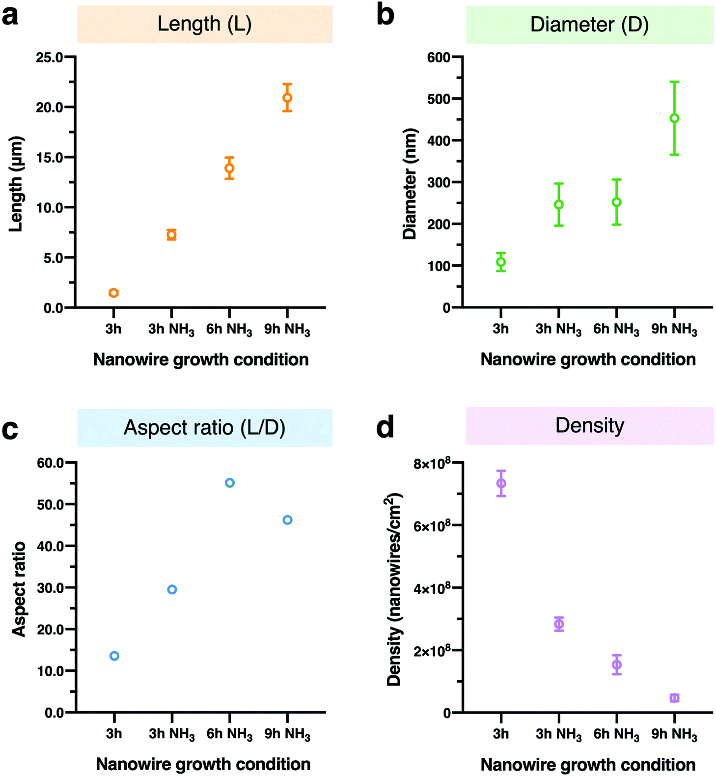 | ||
| Fig. 2 The dependence of the morphology of ZnO nanowires on four nanowire characteristics. (a) Statistic length and (b) diameter of nanowires. The error bars are defined by standard deviation values (n = 100). (c) Aspect ratio (length/diameter) of nanowires. (d) Density of nanowires calculated by counting the tips of nanowires in a known area. The error bars are defined by standard deviation values (n = 490, 190, 100, 30 counted nanowires at each condition, respectively). | ||
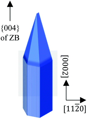
Since the morphological changes to the nanowires are expected to have a significant effect on the crystal structure of the nanowires, we next examined the crystallinity of the nanowires with different morphologies synthesized under each growth condition. Normalized XRD spectra showed the single crystallinity of these nanowires; however different preferential orientations were observed (Fig. 3a). The three main characteristic peaks (100), (002), (101) of wurtzite ZnO phase in the 2θ = 31° to 37° range demonstrated alterations of the dominant ZnO-related peak for each condition (Fig. 3b and Table 1). When ammonia was added for the 3 h growth time, the ZnO nanowires started to grow preferentially in the orientation (101) higher than (002), in contrast, the dominant peak shifted back to (002) direction at 6 h and 9 h with NH3 addition, and the highest intensity (002) peak was observed at 6 h with NH3 addition (Fig. 3c). Besides, the ZnO (004) peak which is the characteristic peak of the cubic zinc blende phase48,49 was observed at 6 h and 9 h with NH3 addition (Fig. 3d). This was attributed to the fact that the synthesis of ZnO nanostructures under a thermodynamic condition generally results in the wurtzite structure since the wurtzite phase is thermodynamically more stable than the zinc blende phase.50 However, compared with the wurtzite ZnO phase, zinc blende ZnO has lower ionicity and higher crystallographic symmetry, and zinc blende ZnO is expected to have higher carrier mobility and electrical gain.48 The presence of different phases in the nanowires may play a role in the capture of EVs by these nanowires, because the chemical and physical properties of nanowires are expected to be significantly influenced by their crystal structure. The above results clearly showed that the effect of ammonia occurred not only on the morphology of the ZnO nanowires but also on their crystallinity, especially in the growth rate of ZnO nanowires in the vertical c-axis direction, where the NH3 addition for 6 h had the highest growth rate.
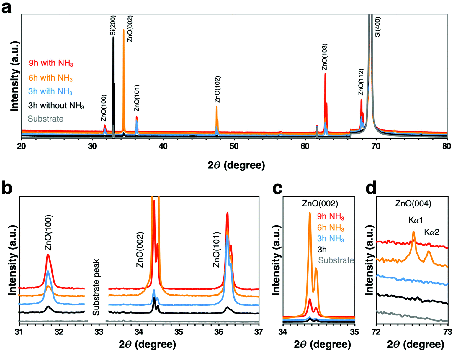 | ||
| Fig. 3 (a) Normalized full spectra XRD patterns. (b) Main characteristic peaks of ZnO wurtzite phase. (c) Enlarged ZnO (002) plane. (d) Enlarged ZnO (004) plane. | ||
| Sample | Peaks ratio | ||
|---|---|---|---|
| (002)/(100) | (002)/(101) | (100)/(101) | |
| 3 h without NH3 | 1.7 | 1.8 | 1.1 |
| 3 h with NH3 | 0.6 | 0.3 | 0.5 |
| 6 h with NH3 | 23.6 | 6.9 | 0.3 |
| 9 h with NH3 | 2.1 | 1.1 | 0.5 |
| 6 h with NH3 500 °C | 2.1 | 0.7 | 0.3 |
The differences in local crystallinity caused by the nanowire morphological change in the upper, middle, and lower regions were investigated (Fig. 4), because the nanowires grown with NH3 additions were found to have a needle-like shape, with the upper part of the nanowires being sharper and smaller in diameter than the lower part. Electron diffraction patterns indicated that the structures of ZnO nanowires with different morphologies synthesized under each growth condition were a single crystal. In case of 3 h growth without NH3 addition, the nanowires grow mainly only along the (0002) direction without any significant lateral sidewall growth for all positions. For the 3 h growth with NH3 addition, the nanowires tended to have varying diameters from upper to lower parts but the selective area electron diffraction (SAED) measurements yielded consistent diffraction patterns. Distinct patterns among the nanowire regions were identified for the cases of 6 and 9 h growth with NH3 addition. At the short 3 h growth time, the wurtzite growth mode was dominant; whereas, the larger diameter nanowires grown with longer reaction times (6 h and 9 h) had a zinc blende crystal structure. In other words, a transition to the zinc blende growth mode occurred at longer times. We investigated the inter planar spacing and diffraction planes from XRD and HRTEM for further understanding of the crystal structure of the nanowires (Table 2).
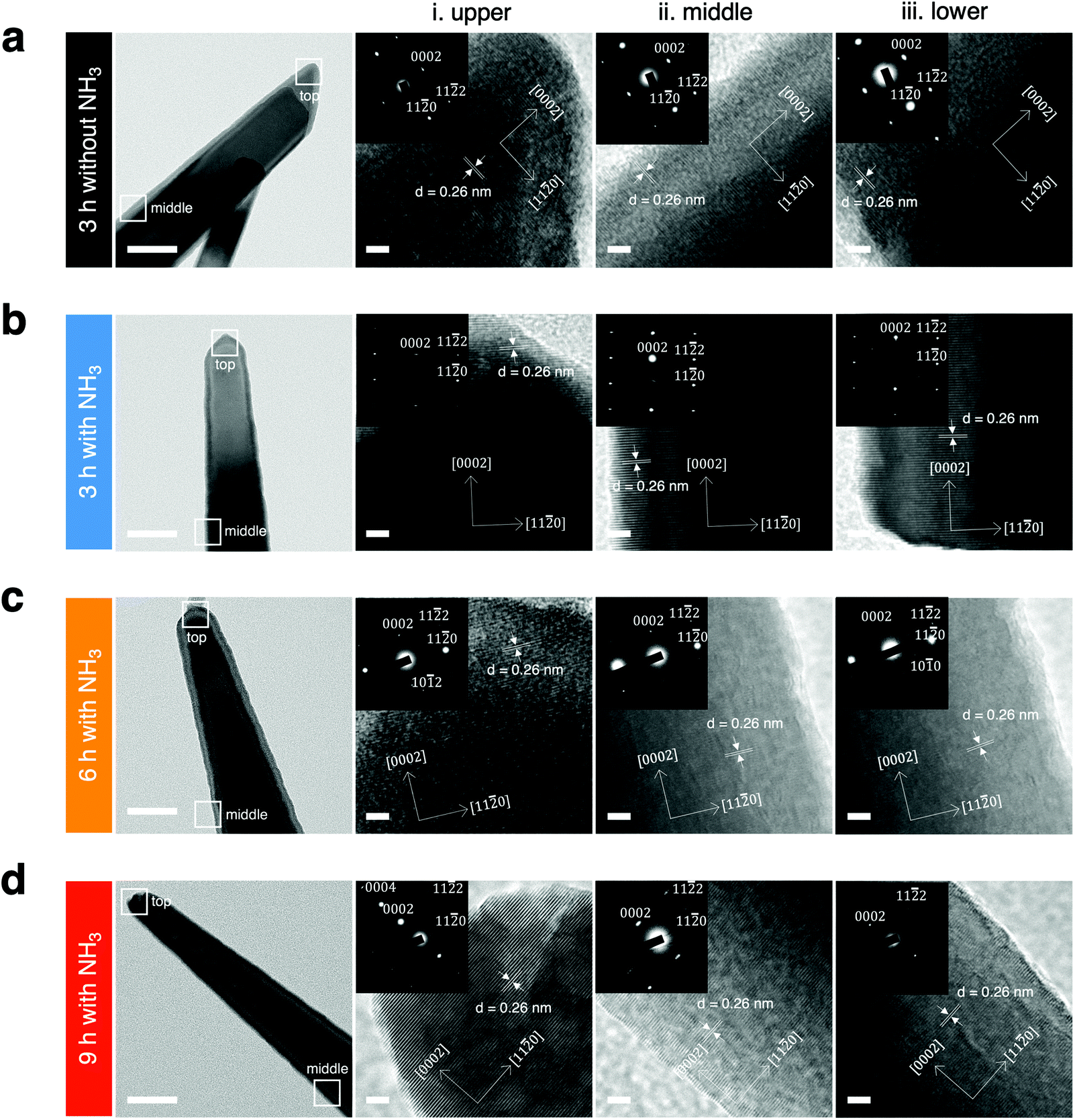 | ||
| Fig. 4 (a–d) Low-resolution TEM images, and HRTEM images in three regions of i. upper, ii. middle and iii. lower of a single ZnO nanowire, where (a) is a nanowire grown for 3 h without NH3 addition; (b) is a nanowire grown for 3 h with NH3 addition; (c) is a nanowire grown for 6 h with NH3 addition; and (d) is a nanowire grown for 9 h with NH3 addition. The insets are SAED patterns of each HRTEM micrograph. The scale bars are 50 nm and 2 nm in low-resolution TEM and HRTEM images, respectively. | ||
| Sample | Peak 2θ | d-Spacing calculated from XRD (nm) | d-Spacing calculated from HRTEM (nm) | Hkl | Structure | |
|---|---|---|---|---|---|---|
| 3 h without NH3 | Upper | 34.37 | 0.2609 | 0.2598 | 002 |
|
| 56.31 | 0.1634 | 0.1602 | 110 | |||
| 67.91 | 0.1380 | 0.1359 | 112 | |||
| Middle | 34.37 | 0.2609 | 0.2570 | 002 | ||
| 56.31 | 0.1634 | 0.1591 | 110 | |||
| 67.91 | 0.1380 | 0.1352 | 112 | |||
| Lower | 34.37 | 0.2609 | 0.2570 | 002 | ||
| 56.31 | 0.1634 | 0.1580 | 110 | |||
| 67.91 | 0.1380 | 0.1352 | 112 | |||
| 3 h with NH3 | Upper | 34.37 | 0.2609 | 0.2598 | 002 |
|
| 56.31 | 0.1634 | 0.1602 | 110 | |||
| 67.91 | 0.1380 | 0.1359 | 112 | |||
| Middle | 34.37 | 0.2609 | 0.2598 | 002 | ||
| 56.31 | 0.1634 | 0.1591 | 110 | |||
| 67.91 | 0.1380 | 0.1359 | 112 | |||
| Lower | 34.37 | 0.2609 | 0.2598 | 002 | ||
| 56.31 | 0.1634 | 0.1602 | 110 | |||
| 67.91 | 0.1380 | 0.1352 | 112 | |||
| 6 h with NH3 | Upper | 34.37 | 0.2609 | 0.2584 | 002 |
|
| 47.49 | 0.1914 | 0.1897 | 102 | |||
| 56.31 | 0.1634 | 0.1596 | 110 | |||
| 67.91 | 0.1380 | 0.1371 | 112 | |||
| Middle | 34.37 | 0.2609 | 0.2635 | 002 | ||
| 56.31 | 0.1634 | 0.1577 | 110 | |||
| 67.91 | 0.1380 | 0.1363 | 112 | |||
| Lower | 31.28 | 0.2859 | 0.2887 | 100 | ||
| 34.37 | 0.2609 | 0.2488 | 002 | |||
| 56.31 | 0.1634 | 0.1585 | 110 | |||
| 67.91 | 0.1380 | 0.1363 | 112 | |||
| 9 h with NH3 | Upper | 34.37 | 0.2609 | 0.2562 | 002 |
|
| 56.31 | 0.1634 | 0.1602 | 110 | |||
| 67.91 | 0.1380 | 0.1352 | 112 | |||
| 72.52 | 0.1303 | 0.1294 | 004 | |||
| Middle | 34.37 | 0.2609 | 0.2555 | 002 | ||
| 56.31 | 0.1634 | 0.1577 | 110 | |||
| 67.91 | 0.1380 | 0.1365 | 112 | |||
| Lower | 36.21 | 0.2480 | 0.2436 | 101 | ||
| 47.49 | 0.1914 | 0.1886 | 102 | |||
The above results highlighted that the growth time with NH3 addition not only affected the lateral diameter but also the growth direction and crystal plane. The anisotropic growth structure of the nanowires is caused by the highest growth rate occurring along the c-axis, which has a high surface energy but a small area leading to the wire-like structures.51 A possible explanation for the wurtzite phase in the nanowires is that side walls of wurtzite have a lower surface energy than the zinc blende nanowires,52–54 and the successful phase transition we achieved was attributed to alterations in nanowire surface energy at different growth conditions with NH3 addition (Fig. S6b†). Although the difference in atomic arrangement on a nanoscale is subtle, it is expected to cause a large difference in the physical and chemical properties of the nanomaterials, such as their EV capture efficiency.55,56 We anticipated that the preferential capture of the negatively charged EVs14,43,57 onto the positively charged surfaces with different crystal planes of ZnO nanowires would lead to the higher EV capture efficiency.
Finally, we demonstrated the effect on EV capture capability for ZnO nanowires fabricated by the ammonia-assisted hydrothermal growth. To do this, we integrated nanowires with PDMS microchannels to fabricate nanowire microfluidic devices (Fig. 5a). The experimental setup of a double-channel nanowire microfluidic device connected with an automatically continuous flow syringe pump supplied EVs into the device (Fig. S5†). The nanowires grown with NH3 additions resulted in the efficacy of EV capture being increased. Further, the nanowires grown for 6 h, with the highest aspect ratio, achieved the highest performance of 68% after which the efficacy dropped at 9 h (Fig. 5b and c). The FESEM images visualizing EVs on the ZnO nanowire surface after the EV capture experiment showed that EVs were directly captured along the nanowire surface (Fig. 5e). We attributed the efficacy enhancement to the fact that nanowires which were long in the vertical could interact with each EV species; however, the capture rate did not increase monotonically within this regime. This was due to the decreased density of nanowires (Fig. 2d), which resulted in fewer possibilities for capture events of EVs onto nanowire surfaces.
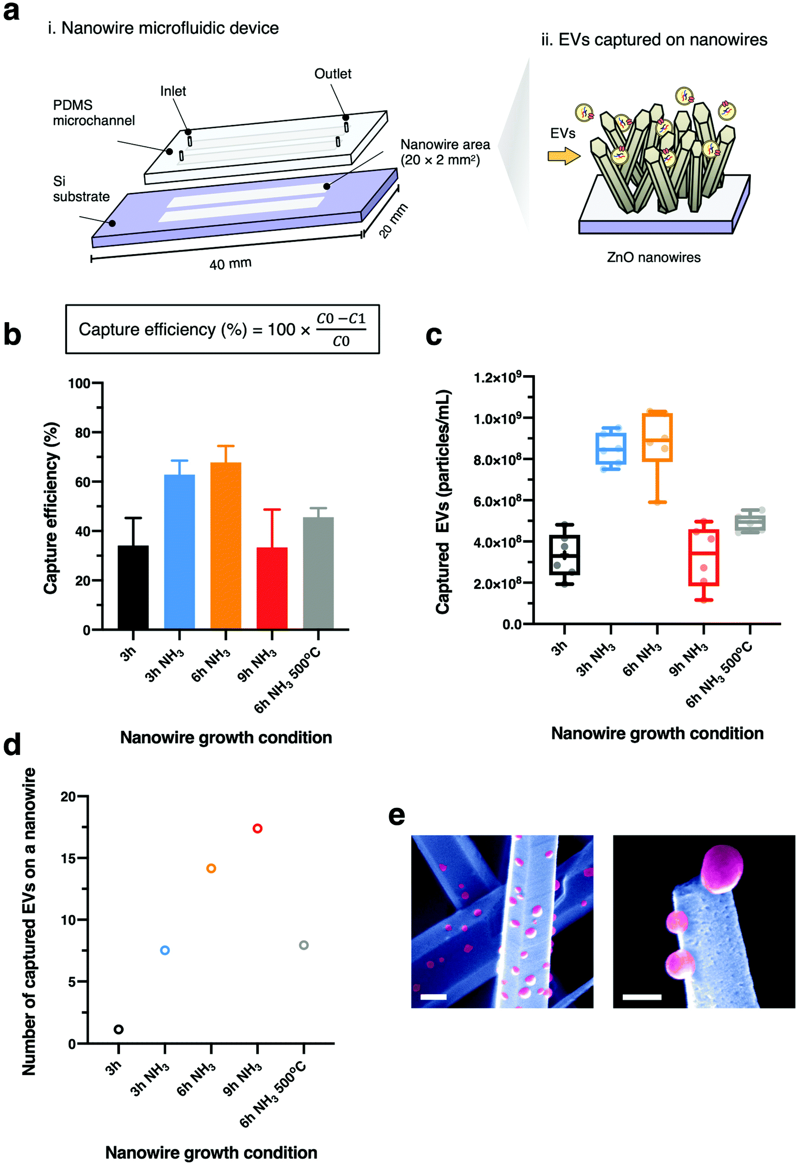 | ||
| Fig. 5 (a) Schematic images of the nanowire microfluidic device and EVs captured by nanowires. (b) The comparative EV capture efficiency and (c) NTA-based numbers of captured vesicles obtained using ZnO nanowire devices. Initial concentration of EVs was 1.0 × 10⁹ (particles per mL). Error bars indicate the standard deviation (n = 6). (d) The comparative capture capacity per unit area of a nanowire for each nanowire condition. (e) Colored FESEM images visualize the adsorption of EVs (pink) on a ZnO nanowire surface (blue) after the EV capture experiment from 6 h with NH3 and 3 h without NH3 conditions, respectively. Scale bars are 100 nm. | ||
In addition to the change in EV capture efficiency due to nanowire morphological changes, we also found a change in EV capture efficiency due to changes in nanowire crystallinity. The nanowires grown with NH3 addition for 9 h showed the lowest capture efficiency due to the low density of the nanowires, but the contribution of a single nanowire to EV capture was qualitatively found to be the highest, indicating that changes in the crystallinity of the nanowires were also important (Fig. 5d). To confirm the effect of the nanowire crystallinity on EV capture, we prepared ZnO nanowires of wurtzite ZnO phase with the same morphology by annealing the nanowires at 500 °C for 2 h (ref. 58–60) after nanowire growth since this annealing process is known to cause the phase transition from zinc blende to wurtzite (Fig. S6a† and Table 1). The nanowires grown with NH3 addition for 6 h followed by the annealing process exhibited lower EV capture efficiency than those grown without the annealing process (Fig. 5b and c). And also, the contribution of a single nanowire to EV capture showed that annealing process significantly decreased the number of captured EVs on a single nanowire, and then the zinc blende phase increased the number of captured EVs on a single nanowire (Fig. 5d and Table 2). Our results highlighted that designing and controlling the crystal structure of ZnO nanowires could be achieved by using NH3 addition to enhance the capability for label-free capture of EVs via the variations of their electrostatic interactions with the ZnO crystal plane. However, NH3 addition and the growth time also affected the morphology of nanowires leading to lower efficiency as the nanowires being larger in diameter and lower in density. Further studies are needed in order to achieve the optimum crystal structure and morphologies of nanowires for a specific application.
Conclusions
This is the first study to identify the effects of crystallinity and morphology of ZnO nanowires grown hydrothermally with NH3 addition on their electrostatic properties for capturing of EVs. As found from results of the XRD and HRTEM analyses, the crystal structures of all samples had the main characteristics of the ZnO wurtzite phase, but they were also mixed with zinc blende phase when grown under some conditions, making them suitable for EV capture on the nanowires. Considering the crystallinity and the morphology of the nanowires, the nanowires grown for 6 h with NH3 addition offered the highest EV capture performance due to the presence of zinc blende phase and high density of the nanowires. These findings are expected to facilitate the realization of tunable nanowires with high potential suitability for integration into advanced label-free EV capture devices which will open up opportunities for further fundamental studies (i.e., adsorption mechanisms by biomolecules) and alternative applications in high-performance integrated nanowire devices.Author contributions
P. Paisrisarn contributed to conceptualization, formal analysis, investigation, methodology, visualization, writing – original draft and writing–review & editing. T. Yasui contributed to conceptualization, funding acquisition, methodology, project administration, supervision and writing–review & editing. Z. Zhu contributed to formal analysis, investigation and methodology. A. Klamchuen contributed to project administration, resources and supervision. P. Kasamechonchung, T. Wutikhun and V. Yordsri contributed to formal analysis, investigation and methodology. Y. Baba contributed to conceptualization, funding acquisition, project administration and supervision.Conflicts of interest
There are no conflicts to declare.Acknowledgements
This research was supported by the Japan Science and Technology Agency (JST) PRESTO (JPMJPR19H9), JST SICORP (JPMJSC19E3), the New Energy and Industrial Technology Development Organization (NEDO) JPNP20004, the JSPS Grant-in-Aid for Scientific Research (S) 18H05243, the JSPS Grant-in-Aid for Scientific Research (B) 21H01960, the JSPS Grant-in-Aid for Exploratory Research 20K21124, the JSPS Grant-in-Aid for Transformative Research Area (A) 21H05778, the JSPS Grant-in-Aid for Scientific Research on Innovative Areas “Chemistry for Multimolecular Crowding Biosystems”, a Medical Research and Development Program (AMED grand no. JP21he2302007 and JP21zf0127004) and research grants from each of the following: Advanced Technology Institute Research grants 2019, the Nanotechnology Platform Program (Molecule and Material Synthesis) of the Ministry of Education, Culture, Sports, Science and Technology (MEXT), and the Cooperative Research Program of the “Network Joint Research Center for Materials and Devices”.Notes and references
- R. G. Hobbs, N. Petkov and J. D. Holmes, Chem. Mater., 2012, 24, 1975–1991 CrossRef CAS.
- B. Tian, T. J. Kempa and C. M. Lieber, Chem. Soc. Rev., 2009, 38, 16–24 RSC.
- N. P. Dasgupta, J. W. Sun, C. Liu, S. Brittman, S. C. Andrews, J. Lim, H. W. Gao, R. X. Yan and P. D. Yang, Adv. Mater., 2014, 26, 2137–2184 CrossRef CAS PubMed.
- P. C. McIntyre and A. F. i Morral, Mater. Today Nano, 2020, 9, 100058 CrossRef.
- V. Gerbreders, M. Krasovska, E. Sledevskis, A. Gerbreders, I. Mihailova, E. Tamanis and A. Ogurcovs, CrystEngComm, 2020, 22, 1346–1358 RSC.
- P. Ambhorkar, Z. Wang, H. Ko, S. Lee, K.-I. Koo, K. Kim and D.-I. D. Cho, Micromachines, 2018, 9, 679 CrossRef PubMed.
- N. Caicedo, R. Leturcq, J.-P. Raskin, D. Flandre and D. Lenoble, Sens. Actuators, B, 2019, 297, 126602 CrossRef CAS.
- B. Tian and C. M. Lieber, Chem. Rev., 2019, 119, 9136–9152 CrossRef CAS PubMed.
- A. M. Nahhas, Am. J. Nanomater., 2021, 8, 18–31 CrossRef.
- T. Yasui, T. Yanagida, S. Ito, Y. Konakade, D. Takeshita, T. Naganawa, K. Nagashima, T. Shimada, N. Kaji, Y. Nakamura, I. A. Thiodorus, Y. He, S. Rahong, M. Kanai, H. Yukawa, T. Ochiya, T. Kawai and Y. Baba, Sci. Adv., 2017, 3, e1701133 CrossRef PubMed.
- T. Suwatthanarak, I. A. Thiodorus, M. Tanaka, T. Shimada, D. Takeshita, T. Yasui, Y. Baba and M. Okochi, Lab Chip, 2021, 21, 597 RSC.
- M. Musa, T. Yasui, Z. Zhu, K. Nagashima, M. Ono, Q. Liu, H. Takahashi, T. Shimada, A. Arima, T. Yanagida and Y. Baba, Anal. Sci., 2021, 37, 1139–1145 CrossRef CAS PubMed.
- H. Takahashi, T. Yasui, H. Kashida, K. Makino, K. Shinjo, Q. Liu, T. Shimada, S. Rahong, N. Kaji, H. Asanuma and Y. Baba, Nanotechnology, 2021, 32, 255301 CrossRef CAS PubMed.
- T. Yasui, P. Paisrisarn, T. Yanagida, Y. Konakade, Y. Nakamura, K. Nagashima, M. Musa, I. A. Thiodorus, H. Takahashi, T. Naganawa, T. Shimada, N. Kaji, T. Ochiya, T. Kawai and Y. Baba, Biosens. Bioelectron., 2021, 194, 113589 CrossRef CAS PubMed.
- H. Takahashi, T. Yasui, A. Klamchuen, N. Khemasiri, T. Wuthikhun, P. Paisrisarn, K. Shinjo, Y. Kitano, K. Aoki, A. Natsume, S. Rahong and Y. Baba, Nanomaterials, 2021, 11, 1768 CrossRef CAS PubMed.
- Y. He, T. Yanagida, K. Nagashima, F. W. Zhuge, G. Meng, B. Xu, A. Klamchuen, S. Rahong, M. Kanai, X. M. Li, M. Suzuki, S. Kai and T. Kawai, J. Phys. Chem. C, 2013, 117, 1197–1203 CrossRef CAS.
- V. Strano, R. G. Urso, M. Scuderi, K. O. Iwu, F. Simone, E. Ciliberto, C. Spinella and S. Mirabella, J. Phys. Chem. C, 2014, 118, 28189–28195 CrossRef CAS.
- P. Kasamechonchung, M. Horprathum, K. Boonpavanitchakul, N. Supaka, P. Prompinit, W. Kangwansupamonkon, A. Somboonkaew, J. Wetcharungsri, S. Pratontep, S. Porntheeraphat and A. Klamchuen, Phys. Status Solidi A, 2015, 212, 394–400 CrossRef CAS.
- Q. Huang, L. Fang, X. Chen and M. R. Saleem, J. Alloys Compd., 2011, 509, 9456–9459 CrossRef CAS.
- L.-Y. Chen, Y.-T. Yin, C.-H. Chen and J.-W. Chiou, J. Phys. Chem. C, 2011, 115, 20913–20919 CrossRef CAS.
- T. Demes, C. Ternon, F. Morisot, D. Riassetto, M. Legallais, H. Roussel and M. Langlet, Appl. Surf. Sci., 2017, 410, 423–431 CrossRef CAS.
- R. Hao, X. Deng, J. Zhang, H. Jang, Y. Zeng and H. Guo, Proc. 2017 Symp. Piezoelectricity Acoust. Waves Device Appli. SPAWDA, 2017, 345–349 Search PubMed.
- R. Parize, J. D. Garnier, E. Appert, O. Chaix-Pluchery and V. Consonni, ACS Omega, 2018, 3, 12457–12464 CrossRef CAS PubMed.
- J. Liu, K. Nagashima, H. Yamashita, W. Mizukami, J. Uzuhashi, T. Hosomi, M. Kanai, X. Zhao, Y. Miura, G. Zhang, T. Takahashi, M. Suzuki, D. Sakai, B. Samransuksamer, Y. He, T. Ohkubo, T. Yasui, Y. Aoki, J. C. Ho, Y. Baba and T. Yanagida, Commun. Mater., 2020, 1, 58 CrossRef.
- J. Joo, B. Y. Chow, M. Prakash, E. S. Boyden and J. M. Jacobson, Nat. Mater., 2011, 10, 596–601 CrossRef CAS PubMed.
- T. H. Kwon, K. Kim, S. H. Park, A. A. Annamalai and M. J. Lee, Int. J. Nanotechnol., 2013, 10, 681 CrossRef CAS.
- L. Liu, K. Hong, X. Ge, D. Liu and M. Xu, J. Phys. Chem. C, 2014, 118, 15551–15555 CrossRef CAS.
- R. Kumar, O. Al-Dossary, G. Kumar and A. Umar, Nano-Micro Lett., 2015, 7, 97–120 CrossRef PubMed.
- J. Wang, X. Li, C. Teng, Y. Xia, J. Xu, D. Xie, L. Xiang and S. Komarneni, J. Mater. Chem. C, 2016, 4, 5755–5765 RSC.
- S. V. Kurudirek, K. C. Pradel and C. J. Summers, J. Alloys Compd., 2017, 702, 700–709 CrossRef CAS PubMed.
- A. C. Campos, S. C. Paes, B. S. Correa, G. A. Cabrera-Pasca, M. S. Costa, C. S. Costa, L. Otubo and A. W. Carbonari, ACS Appl. Nano Mater., 2020, 3, 175–185 CrossRef CAS.
- M. Yanez-Mo, P. R. Siljander, Z. Andreu, A. B. Zavec, F. E. Borras, E. I. Buzas, K. Buzas, E. Casal, F. Cappello, J. Carvalho, E. Colas, A. Cordeiro-da Silva, S. Fais, J. M. Falcon-Perez, I. M. Ghobrial, B. Giebel, M. Gimona, M. Graner, I. Gursel, M. Gursel, N. H. Heegaard, A. Hendrix, P. Kierulf, K. Kokubun, M. Kosanovic, V. Kralj-Iglic, E. M. Kramer-Albers, S. Laitinen, C. Lasser, T. Lener, E. Ligeti, A. Line, G. Lipps, A. Llorente, J. Lotvall, M. Mancek-Keber, A. Marcilla, M. Mittelbrunn, I. Nazarenko, E. N. M. N. Hoen, T. A. Nyman, L. O’Driscoll, M. Olivan, C. Oliveira, E. Pallinger, H. A. Del Portillo, J. Reventos, M. Rigau, E. Rohde, M. Sammar, F. Sanchez-Madrid, N. Santarem, K. Schallmoser, M. S. Ostenfeld, W. Stoorvogel, R. Stukelj, S. G. Van der Grein, M. H. Vasconcelos, M. H. Wauben and O. De Wever, J. Extracell. Vesicles, 2015, 4, 27066 CrossRef PubMed.
- G. van Niel, G. D'Angelo and G. Raposo, Nat. Rev. Mol. Cell Biol., 2018, 19, 213–228 CrossRef CAS PubMed.
- L. M. Doyle and M. Z. Wang, Cells, 2019, 8, 727 CrossRef CAS PubMed.
- R. Xu, A. Rai, M. Chen, W. Suwakulsiri, D. W. Greening and R. J. Simpson, Nat. Rev. Clin. Oncol., 2018, 15, 617–638 CrossRef CAS PubMed.
- L. Han, E. W. F. Lam and Y. Sun, Mol. Cancer, 2019, 18, 59 CrossRef PubMed.
- Y. Gao, Y. Qin, C. Wan, Y. Sun, J. Meng, J. Huang, Y. Hu, H. Jin and K. Yang, Front. Oncol., 2021, 11, 638357 CrossRef PubMed.
- L. K. Chin, T. Son, J.-S. Hong, A.-Q. Liu, J. Skog, C. M. Castro, R. Weissleder, H. Lee and H. Im, ACS Nano, 2020, 14, 14528–14548 CrossRef PubMed.
- S. Sharma, M. K. Masud, Y. V. Kaneti, P. Rewatkar, A. Koradia, M. S. A. Hossain, Y. Yamauchi, A. Popat and C. Salomon, Small, 2021, 17, e2102220 CrossRef PubMed.
- Z. Zhuo, J. Wang, Y. Luo, R. Zeng, C. Zhang, W. Zhou, K. Guo, H. Wu, W. Sha and H. Chen, Acta Biomater., 2021, 134, 13–31 CrossRef CAS PubMed.
- A. Hoshino, B. Costa-Silva, T.-L. Shen, G. Rodrigues, A. Hashimoto, M. T. Mark, H. Molina, S. Kohsaka, A. Di Giannatale, S. Ceder, S. Singh, C. Williams, N. Soplop, K. Uryu, L. Pharmer, T. King, L. Bojmar, A. E. Davies, Y. Ararso, T. Zhang, H. Zhang, J. Hernandez, J. M. Weiss, V. D. Dumont-Cole, K. Kramer, L. H. Wexler, A. Narendran, G. K. Schwartz, J. H. Healey, P. Sandstrom, K. J. Labori, E. H. Kure, P. M. Grandgenett, M. A. Hollingsworth, M. de Sousa, S. Kaur, M. Jain, K. Mallya, S. K. Batra, W. R. Jarnagin, M. S. Brady, O. Fodstad, V. Muller, K. Pantel, A. J. Minn, M. J. Bissell, B. A. Garcia, Y. Kang, V. K. Rajasekhar, C. M. Ghajar, I. Matei, H. Peinado, J. Bromberg and D. Lyden, Nature, 2015, 527, 329–335 CrossRef CAS PubMed.
- S. A. Melo, L. B. Luecke, C. Kahlert, A. F. Fernandez, S. T. Gammon, J. Kaye, V. S. LeBleu, E. A. Mittendorf, J. Weitz, N. Rahbari, C. Reissfelder, C. Pilarsky, M. F. Fraga, D. Piwnica-Worms and R. Kalluri, Nature, 2015, 523, 177–182 CrossRef CAS PubMed.
- H. Zhang, D. Freitas, H. S. Kim, K. Fabijanic, Z. Li, H. Chen, M. T. Mark, H. Molina, A. B. Martin, L. Bojmar, J. Fang, S. Rampersaud, A. Hoshino, I. Matei, C. M. Kenific, M. Nakajima, A. P. Mutvei, P. Sansone, W. Buehring, H. Wang, J. P. Jimenez, L. Cohen-Gould, N. Paknejad, M. Brendel, K. Manova-Todorova, A. Magalhães, J. A. Ferreira, H. Osório, A. M. Silva, A. Massey, J. R. Cubillos-Ruiz, G. Galletti, P. Giannakakou, A. M. Cuervo, J. Blenis, R. Schwartz, M. S. Brady, H. Peinado, J. Bromberg, H. Matsui, C. A. Reis and D. Lyden, Nat. Cell Biol., 2018, 20, 332–343 CrossRef CAS PubMed.
- C. Xu, P. Shin, L. Cao and D. Gao, J. Phys. Chem. C, 2010, 114, 125–129 CrossRef CAS.
- Q. L. Liu, T. Yasui, K. Nagashima, T. Yanagida, M. Hara, M. Horiuchi, Z. T. Zhu, H. Takahashi, T. Shimada, A. Arima and Y. Baba, J. Phys. Chem. C, 2020, 124, 20563–20568 CrossRef CAS.
- M. Law, L. E. Greene, J. C. Johnson, R. Saykally and P. D. Yang, Nat. Mater., 2005, 4, 455–459 CrossRef CAS PubMed.
- Y. Y. Zhang, M. K. Ram, E. K. Stefanakos and D. Y. Goswami, J. Nanomater., 2012, 2012, 624520 Search PubMed.
- A. Ashrafi and C. Jagadish, J. Appl. Phys., 2007, 102, 071101 CrossRef.
- N. Munoz-Aguirre, L. Martinez-Perez, S. Munoz-Aguirre, L. A. Flores-Herrera, E. V. Hernandez and O. Zelaya-Angel, Materials, 2019, 12, 3314 CrossRef CAS PubMed.
- X. Huang, M. G. Willinger, H. Fan, Z. L. Xie, L. Wang, A. Klein-Hoffmann, F. Girgsdies, C. S. Lee and X. M. Meng, Nanoscale, 2014, 6, 8787–8795 RSC.
- S. Boubenia, A. S. Dahiya, G. Poulin-Vittrant, F. Morini, K. Nadaud and D. Alquier, Sci. Rep., 2017, 7, 15187 CrossRef CAS PubMed.
- H. J. Joyce, J. Wong-Leung, Q. Gao, H. H. Tan and C. Jagadish, Nano Lett., 2010, 10, 908–915 CrossRef CAS PubMed.
- K. Ikejiri, Y. Kitauchi, K. Tomioka, J. Motohisa and T. Fukui, Nano Lett., 2011, 11, 4314–4318 CrossRef CAS PubMed.
- A. Jenichen, C. Engler and B. Rauschenbach, Surf. Sci., 2013, 613, 74–79 CrossRef CAS.
- M. Ghosh, D. Karmakar, S. Basu, S. N. Jha, D. Bhattacharyya, S. C. Gadkari and S. K. Gupta, J. Phys. Chem. Solids, 2014, 75, 543–549 CrossRef CAS.
- K. Momeni and H. Attariani, Phys. Chem. Chem. Phys., 2014, 16, 4522–4527 RSC.
- G. Midekessa, K. Godakumara, J. Ord, J. Viil, F. Lättekivi, K. Dissanayake, S. Kopanchuk, A. Rinken, A. Andronowska, S. Bhattacharjee, T. Rinken and A. Fazeli, ACS Omega, 2020, 5, 16701–16710 CrossRef CAS PubMed.
- Z. N. Kayani, F. Saleemi and I. Batool, Appl. Phys. A, 2015, 119, 713–720 CrossRef CAS.
- M. R. Parra and F. Z. Haque, J. Mater. Res. Technol., 2014, 3, 363–369 CrossRef CAS.
- E. Y. Shaba, J. O. Jacob, J. O. Tijani and M. A. T. Suleiman, Appl. Water Sci., 2021, 11, 48 CrossRef CAS.
Footnote |
| † Electronic supplementary information (ESI) available. See DOI: 10.1039/d1nr07237d |
| This journal is © The Royal Society of Chemistry 2022 |