
 Open Access Article
 This Open Access Article is licensed under a
 Creative Commons Attribution 3.0 Unported Licence
Insights into first-principles characterization of the monoclinic VO2(B) polymorph via DFT + U calculation: electronic, magnetic and optical properties
Elaheh
Mohebbi
a,
Eleonora
Pavoni
 a,
Davide
Mencarelli
b,
Pierluigi
Stipa
a,
Luca
Pierantoni
b and
Emiliano
Laudadio
*a
a,
Davide
Mencarelli
b,
Pierluigi
Stipa
a,
Luca
Pierantoni
b and
Emiliano
Laudadio
*a
aDepartment of Materials, Environmental Sciences and Urban Planning, Marche Polytechnic University, 60131 Ancona, Italy. E-mail: e.mohebbi@staff.univpm.it; E.pavoni@staff.univpm.it; p.stipa@staff.univpm.it; E.Laudadio@staff.univpm.it
bInformation Engineering Department, Marche Polytechnic University, 60131 Ancona, Italy. E-mail: l.pierantoni@staff.univpm.it; d.mencarelli@staff.univpm.it
First published on 9th August 2022
Abstract
We have studied the structural, electronic, magnetic, and optical properties of the VO2(B) polymorph using first-principles calculations based on density functional theory (DFT). This polymorph was found to display four optimized structures namely VO2(B)PP, VO2(B)LP, VO2(B)PPD, and VO2(B)LPD using the generalized gradient approximation (GGA) PBE exchange-correlation functional by including/excluding van der Waals interaction. Our derivation provides a theoretical justification for adding an on-site Coulomb U value in the conventional DFT calculations to allow a direct comparison of the two methods. We predicted a zero bandgap of the VO2(B) structure based on GGA/PBE. However, by GGA/PBE + U, we found accurate bandgap values of 0.76, 0.66, and 0.70 eV for VO2(B)PP, VO2(B)LP, and VO2(B)PPD, respectively. The results obtained from DFT + U were accompanied by a structural transition from the metallic to semiconductor property. Here, we verified the non-magnetic characteristic of the monoclinic VO2(B) phase with some available experimental and theoretical data. However, the debate on the magnetic property of this polymorph remains unresolved. Imaginary and real parts of the dielectric function, as computed with the GGA/PBE functional and the GGA/PBE + U functional, were also reported. The first absorption peaks of all considered geometries in the imaginary part of the dielectric constants indicated that the VO2(B) structure could perfectly absorb infrared light. The computed static dielectric constants with positive values, as derived from the optical properties, confirmed the conductivity of this material. Among the four proposed geometries of VO2(B) in this study, the outcomes obtained by VO2(B)PPD reveal good results owing to the excellent consistency of its bandgap, magnetic and optical properties with other experimental and theoretical observations. The theoretical framework in our study will provide useful insight for future practical applications of the VO2(B) polymorph in electronics and optoelectronics.
Introduction
Transition metal oxides1–3 have been widely studied during the last decades because of their unique physical properties that are exploitable in the areas of dielectrics,4,5 thermoelectricity,6–8 catalysis,9–11 microelectronics,12,13 and thin-film transistors.14–18 Vanadium oxides are of particular interest due to these materials provide outstanding advantages in many optoelectronic devices, such as smart windows,19–21 sensors,22–24 and resistive memories.25–29 They have received considerable attention since they are studied as a metal–insulator transition (MIT) material.30–34 The MIT can be induced by increasing the temperature/pressure, which causes changes to the structural, electronic, electrical, and optical properties of the materials.35–42According to experimental and theoretical studies, different structures of vanadium oxides have been found at high and low-temperature phases. So far, VO2,43–46 V2O5,47,48 V2O3,49–51 V3O5,52 V4O7,53 and V6O13 (ref. 54 and 55) are the most interesting compounds with well known structural properties for the MIT. Vanadium dioxides (VO2) are very well known materials with several polymorphs, including tetragonal (R),56 monoclinic (M),57 triclinic (T),58 tetragonal (A),59 monoclinic (B),60 paramontroseite61 and the new body centered-cubic (bcc) structure.62 At a high temperature, a metallic phase (VO2(R)) with a rutile structure can be achieved, while cooling to below 340 K, the R phase changes into an insulating monoclinic structure M phase.63–65 Because the phase transition from the rutile VO2(R) and the monoclinic VO2(M) is associated with a huge change in resistivity, it has attracted considerable attention for electronic and optical applications.43,66–69
VO2(B) has been explored as a promising cathode material in Li ion batteries, mainly because of its prominent advantages of high discharge capacity of 323 mA h g−1 and low cost.70–73 Moreover, the VO2(M) and VO2(R) phases can be prepared by the irreversible transformation of VO2(B) as a precursor.74,75
Advanced theoretical and experimental techniques have been implemented to study the VO2(B) polymorph. While an experimental bandgap of 0.6–0.7 eV (ref. 76–78) was found for VO2 near the semiconductor–metal transition, an X-ray photoelectron spectroscopy study revealed a metallic observation of this material at room temperature.64 In agreement with the experimental results, the first-principles calculations confirmed both metallic and insulating features of VO2(B).64,74,79,80 In the study conducted by Lee et al.,80 XAS, optical spectroscopy, and DFT calculations were applied to assess the bandgap in the VO2(B), VO2(M), and VO2(A) structures. This study revealed that by comparing the electronic structures of the A, B, and M phases, conventional DFT calculations estimated signatures of a metallic behavior for the A, B, and M phases. Meanwhile, hybrid functional calculations indicated bandgaps of 0.6 eV and 0.5 eV for the M and A phases, respectively, and a very narrow bandgap of 25 meV for the B phase. Zhang et al.74 investigated the phase transition process from VO2(B) to VO2(A) based on X-ray absorption spectroscopy (XAS) analysis and DFT calculations. They reported on the metastability of VO2(B) in comparison with the VO2(A) and VO2(R) phases. The calculation of the formation energy in a different phase of VO2 showed that the VO2(B) structure has less geometrical stability with −6.66 eV formation energy compared to −6.93 and −7.18 eV for VO2(R) and VO2(M), respectively. This study proposed that the different electronic structure completely depended on the different stabilities of the VO2 phases. In a recent study carried out by Popuri et al.,81 the electron transport properties of the VO2(B) structure at low (25–200 K), intermediate (200–320 K), and high temperatures (320–350 K) were investigated using spark plasma sintering. They found different electronic and magnetic properties at different thermal phases. At the low and intermediate temperature phases, nonmagnetic ordering was associated with the insulating characteristic of the structure. At a high temperature, metallic behavior and antiferromagnetic property were observed. In another study, Lourembam et al.82 used terahertz time-domain spectroscopy (THz-TDS) to investigate the temperature-dependent complex optical conductivity of the VO2(B) structure. They observed that VO2(B) transformed from an insulating system to a conducting system at 240 K. Furthermore, there was a broad intermediate state with the transition onset being much closer to room temperature, allowing this polymorph to be more suitable for optoelectronic devices near room temperature. In an extensive experimental and theoretical research recently conducted by Wan et al.,83 they indicated that pure VO2(B) has weak absorption in infrared light, with excellent agreement between theory and experiment.
So far, some experimental results have been determined for the geometrical data and MIT for this compound.82–88 The electronic properties have been investigated with some experimental and theoretical methodologies; however, the data are still limited and variable.64,74,79,83,89 Furthermore, magnetic and optical features are potentially important properties that have not yet been systematically studied for this polymorph with first-principles calculations, and no detailed values have been reported yet. Since a systematic investigation of the efficacy of advanced theoretical methods for computing the chemical and physical properties of VO2(B) is missing, our study seeks to fill this gap in the literature. Our present work is focused on the complete theoretical description of the electronic, magnetic, and optical properties of the VO2(B) polymorph using GGA/PBE and GA/PBE + U functionals. Recent studies have shown how the combined use of these methods makes it possible to calculate different material properties.90 The main objectives of this work are as follows: (i) investigation of the structural parameters of VO2(B) by employing different theoretical approaches. The geometry optimization of this polymorph will be assessed by different methodologies in order to find the most accurate results of the material characterization in agreement with the experimental outcomes. (ii) Calculation of the electronic band structure and magnetic properties, (iii) and analysis of the optical properties of the proposed different geometries of VO2(B).
Computational methods
We carried out the atomistic calculations using the Quantum ESPRESSO (QE)91 and QuantumATK (QATK)92 packages. The DFT approach was implemented in the Kohn–Sham (KS) formulation93,94 within the framework of the linear combination of atomic orbitals (LCAO) and plane-wave (PW) basis set approaches, combined with the pseudopotential (PPs) method. PseudoDojo95 and Projector Augmented Wave (PAW) PPs96 were used for the LCAO and PW calculations, respectively, with the aim to describe the interaction between ion cores and valence electrons. DFT-LCAO and DFT-PW calculations were performed within the GGA framework adopting the PBE exchange-correlation (XC) functional.97 Valence orbitals were expanded in a PW basis set with a kinetic energy cut-off of 70 Ry. Brillouin-zone (BZ)98 integrations were limited to the gamma point mesh, and a smearing parameter of 0.0001 Ry was considered for the electron population function.99 The van der Waals corrections were included by the Grimme's DFT-D3 method,100 and the structure was relaxed with the Broyden–Fletcher–Goldfarb–Shanno (BFGS) algorithm.101 We implemented both PBE and PBE + U102,103 in post-processing calculations in order to make an exhaustive comparison between the different geometries. Since previous studies have shown that the outcomes substantially depended on the magnitude of U, we tested different Hubbard U values for the vanadium d orbital (Ud) and oxygen p orbital (Up). In this study, we have set Ud = 5.20 eV and Up = 0.95 eV, wherein they have more similarity to the results reported by Huffman et al.104 (Ud = 5.00 eV and Up = 0.00 eV). However, our chosen Hubbard values show more agreement between the theoretical and experimental bandgaps, as we will discuss later.To calculate the electronic band structure and Projected DOS (PDOS), since the KS equation is a nonlinear differential formula, we first converged the charge density with the self-consistent field (SCF) calculations to compute the DOS on a uniform k-mesh (we used the 6 × 6 × 6 k-points). Then, we ran the non-self-consistent (NSCF) calculation with a twice high k-mesh with respect to the SCF calculations (12 × 12 × 12 Monkhorst–Pack mesh) in order to construct the Hamiltonian for the charge density by using the tetrahedron method. PDOS was also considered to account for the magnetic ordering of the compound. Optical calculations were analyzed based on the random phase approximation (RPA).105,106 The optical properties of the VO2(B) structure in this study are discussed by the two components of the dielectric function (ε(ω) = ε1(ω) + iε2(ω)) related to different polarizations in the electric field. The imaginary part of the dielectric coefficient can be obtained from the direct interband transitions through Fermi's golden rule as:107–109
 | (1) |
 | (2) |
The electron energy loss spectrum, L(ω), can also be described using the dielectric constants by:111,112
 | (3) |
The energy loss function determines the loss of energy while traversing through the material. Molecular graphics were generated using the XCRYSDEN graphical package.113
Results and discussion
Analysis of the polymeric structure
VO2(B) with the space group C2/m was simulated in periodic boundary conditions (PBC) along with three Cartesian coordinates. As shown in Fig. 1, the base-centered monoclinic unit cell has dimensions of 11.85 × 3.74 × 6.49 Å3. This included 12 atoms in the primitive unit cell (4 vanadium and 8 oxygen) and 24 atoms in the conventional unit cell (8 vanadium and 16 oxygen atoms) (see Fig. 1(b)). This unit cell dimension is in good agreement with the previous experimental patterns64,81,85 and theoretical studies.74,79,83 As shown in Fig. 1(a) and (b), the VO2(B) structure can be considered as two identical atom layers including 3D frameworks of VO6 octahedra. These octahedra packings of VO6 are only linked by oxygen atoms in the corners. The second layer is shifted with respect to the first one by 1/2, 1/2, 0. This polymorph is distorted because of the out-of-center vanadium atoms, resulting in the presence of short/long V–V and two different types of octahedra.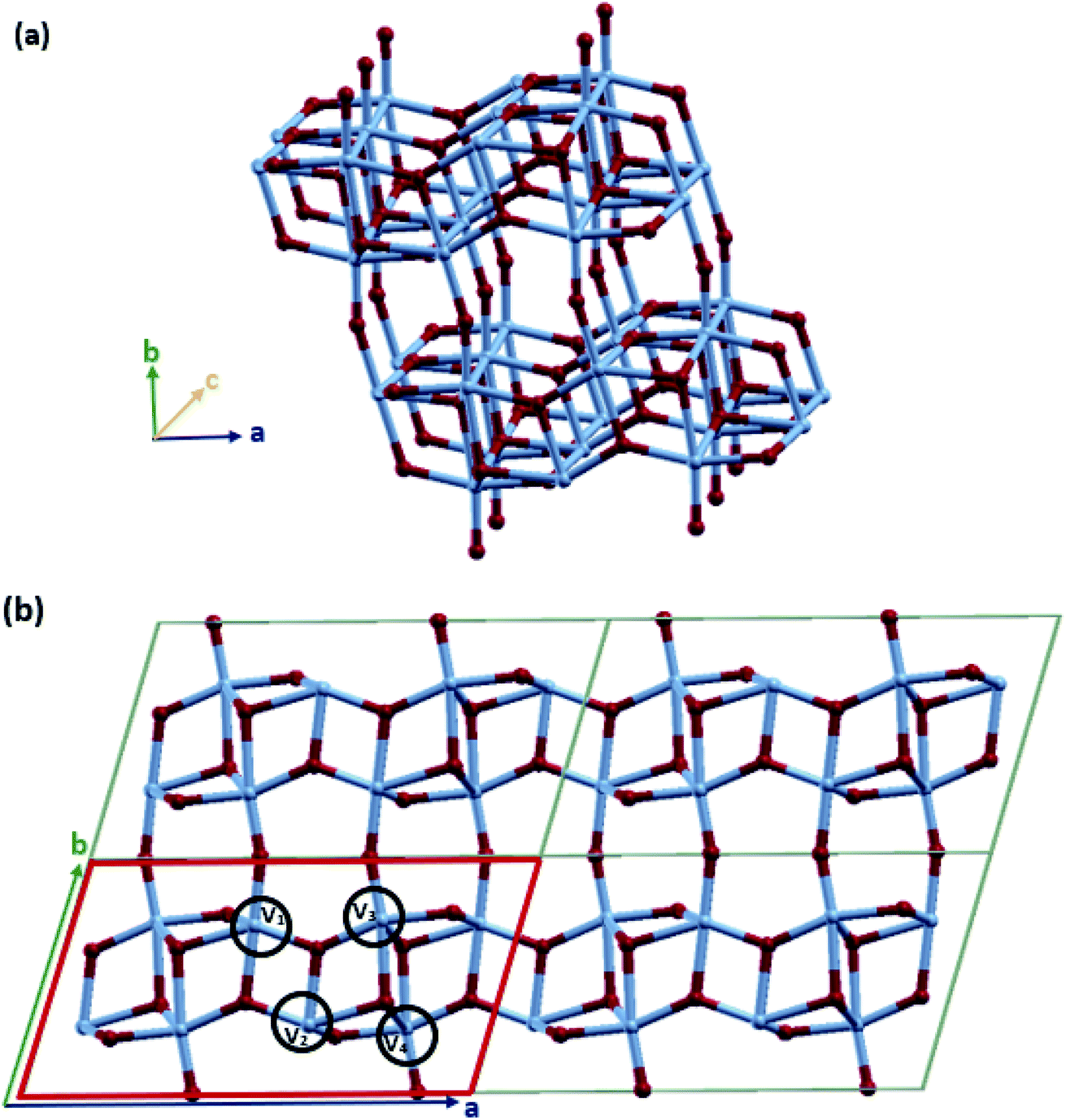 | ||
| Fig. 1 Schematic representations of (a) the 3D frameworks of VO6 octahedra in VO2(B) (b) 2D 2 × 2 supercell of the VO2(B) polymorph, solid red line represents the unit cell of the structure. Color code in the model: V blue and O red. | ||
The lattice energy minimized for VO2(B) was obtained by employing geometry optimizations of the atomic positions and altering the size and angle of the unit cell, systematically. After the optimization of the lattices, we evaluated the structural parameters and bond lengths on different types of vanadium atoms in the 3D structure. As shown in Fig. 1(b), there are 4 types of V–V bonds in the VO2(B) structure. From the experimental bond lengths (see Table 1), they are as follows: (i) the shortest V1–V2 bond in the center of the xy plane with a bond length of 2.89 Å, (ii) V2–V3 vanadium atoms in the xy plane with a length of 3.24 Å, (iii) long V3–V4 vanadium bonds with an average distance of 3.33 Å, and (iv) medium bond length of V1–V4 characterized by 3.06 Å.
| Structural parameters (Å) | PW (PBE) | LCAO (PBE) | PW (PBE-D3) | LCAO (PBE-D3) | Experiment81 |
|---|---|---|---|---|---|
| V1–V2 | 3.33 | 2.81 | 2.98 | 3.02 | 2.89 |
| V2–V3 | 3.79 | 3.27 | 3.34 | 3.32 | 3.24 |
| V3–V4 | 3.18 | 3.45 | 3.50 | 3.55 | 3.33 |
| V1–V4 | 2.94 | 3.05 | 3.18 | 3.17 | 3.06 |
Table 1 indicates that the VO2(B) compound exhibits different ranges of the V–V bond distance with the four optimized geometries obtained from the PW and LCAO approaches by including/excluding the dispersion corrections (DFT-D3) in the GGA/PBE calculations. For the convenience of discussion, the experimental and theoretical V–V bond lengths and their differences are listed in Table 1. In comparison to the experimental results in ref. 81, the VO2(B) optimized structure obtained from the PW approach and PBE XC functional without including the dispersion corrections (PW(PBE)) (the material named VO2(B)PP) exhibited V1 and V3 atoms that were greatly displaced away from the central vanadium atom V2 with V1–V2 = 3.33 Å and V2–V3 = 3.79 Å. Moreover, V4 became closer to V3 and V1 with distances of 3.18 Å and 2.94 Å, respectively. In the case of PW(PBE-D3) (VO2(B)PPD) including the van der Waals interactions, the V1–V2 and V2–V3 bond distances were shortened to 2.98 Å and 3.34 Å in more agreement with the experimental values of 2.89 Å and 3.24 Å, respectively. However, the V3–V4 bond distance reached the length of 3.45 Å, which is far from the experimental distance of 3.33 Å. In the VO2(B)LP structure obtained from the LCAO(PBE) method, the V3–V4 and V1–V4 bond distances were elongated from 3.18 Å and 2.94 Å in VO2(B)PP to 3.45 Å and 3.05 Å in VO2(B)LP, respectively, while the V2–V3 bond distance decreased from 3.79 Å in VO2(B)PP to 3.27 Å in this geometry. In this case, V1 and V2 significantly became closer together by 2.81 Å, which is less than the experimental value of 2.89 Å. Finally, the optimized structure of VO2(B)LPD obtained from LCAO(PBE-D3) including the dispersion corrections exhibited the greatest similarity to the results obtained from VO2(B)PPD with distances V1–V2 = 3.02 Å, V2–V3 = 3.32 Å, V3–V4 = 3.55 Å, and V1–V4 = 3.17 Å.
From the structural parameters computed by the two different PW and LCAO approaches presented in Table 1, we can understand the trend with regards to the treatment of the chosen basis set and XC functional. By using the PW basis set and the PAW XC functional, the approximation tends to overestimate V1–V2 and underestimate V3–V4. Conversely, the LCAO basis set associated with the PseudoDojo XC functional leads to an underestimate of V1–V2 and overestimate of V3–V4. However, including the van der Waals interactions moderated the system in both approximations. From these results, it is important to note that the basis set approximation can have a significant effect on the computed structures. Calculations on the bulk of similar materials have demonstrated that the LCAO approximation tends to give results that agree less with experimental results compared to the PW. In addition, it is worth noting that van der Waals interactions have a remarkable role in reducing the V1–V2 and V2–V3 interlayer distances when we consider our system by the PW basis set (Table 1). Meanwhile, it has the opposite effect when the LCAO basis set is used by enhancing the corresponding bond lengths of V1–V2 and V2–V3. As we shall discuss later, since the shortest V1–V2 bond distance plays a critical role in the electronic structure of the VO2(B) polymorphs, the PW(DFT-D3) method gives us more accurate results related to the different physical properties of the VO2(B) nanostructure.
In the next step, we calculated the post-processing computations of the electronic, magnetic, and optical properties of four different geometries of the VO2(B) polymorph in order to discover which geometry indicates better accordance to experimental and theoretical studies for this material.
Electronic and magnetic properties
We studied the electronic properties of the VO2(B) polymorph by computing the electronic band structure and the corresponding PDOS curves for total, V-3d, and O-2p for VO2(B)PP, VO2(B)LP, VO2(B)PPD, and VO2(B)LPD geometries based on the PBE and PBE + U approximations. The band structure was analyzed along the high symmetry G–M–G–X–Y–I–L–G directions in the first BZ. The results calculated by GGA/PBE revealed the zero bandgap for all four geometries of the VO2(B) polymorph. Since conventional XC functionals such as PBE often underestimate the bandgap in semiconductors,114 we also employed the DFT + U method to provide a more accurate prediction of the V d–d orbital correlations and bandgap. So far, the DFT + U method was successful in the prediction of the bandgap for different polymorphs of vanadium oxides. Furthermore, the outcomes agreed relatively well with experimental results.83,115–118Fig. 2 and 3 describe the band structure and DOS predicted by the PBE + U functional, respectively. From these results, we found that the Hubbard method described the electronic bandgap in VO2(B) well when the U correction effect is considered in DFT. The corresponding bandgap of the VO2(B) geometries based on GGA/PBE + U became much larger, i.e., 0.76 eV, 0.66 eV, and 0.70 eV for VO2(B)PP (a), VO2(B)LP (b), and VO2(B)PPD (c), respectively, leading to the semiconductor character of this material. An inspection of Fig. 3 indicates that with the main contribution of total DOS belonged to the V-3d orbital accompanied by less contribution from the O-2p state. As reported in Fig. 2 and 3 (d), excluding/including the U correction in the PBE calculation showed the same zero bandgap for the VO2(B)LPD geometry. VO2(B)LPD might have a very narrow bandgap. Hence, DFT calculations could not accurately describe the electronic ground states of this structure. Our results from PBE and PBE + U approximations indicate good consistency with the previous experimental and theoretical studies. Our estimated bandgap values by GGA/PBE + U approximation for the optimized structure VO2(B)PP, VO2(B)LP and VO2(B)PPD were fitted with the experimental value of 0.6–0.7 eV,76–78 comparable with 0.65 eV computed by the HSE method,74 and the values predicted by DFT + U (Ud = 4.00 eV) with 0.60 eV83 and 0.78 eV (Ud = 3.25 eV).79 Moreover, the outcomes predicted by Lee et al.80 revealed the narrow bandgap semiconductor (<25 meV) for the VO2(B) structure using the PBE0 hybrid functional.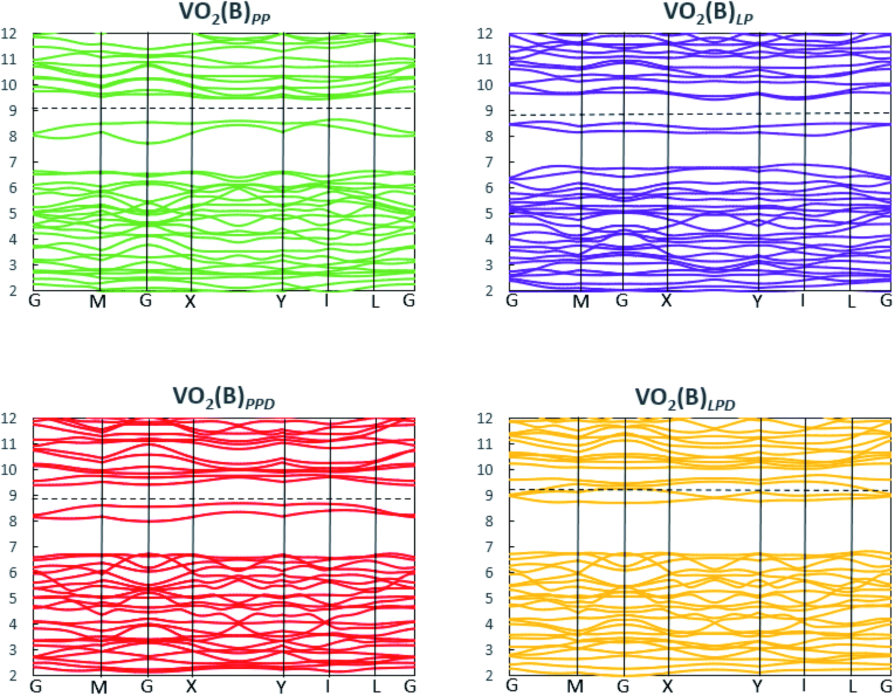 | ||
| Fig. 2 Band structure of VO2(B)PP, VO2(B)LP, VO2(B)PPD, and VO2(B)LPD structures predicted by the GGA/PBE + U functional. Fermi energy aligned in the dash line. | ||
 | ||
| Fig. 3 Total and partial DOS curves for the total, V-3d, and O-2p of VO2(B)PP, VO2(B)LP, VO2(B)PPD, and VO2(B)LPD structures predicted by the GGA/PBE + U functional. Fermi energy aligned in the dash line. | ||
Next, we examined the magnetism ordering of VO2(B) geometries by consideration of the SCF output files and Lowdin charge119,120 analysis from PDOS calculations.
The magnetism has been reported as two values of the total magnetization and absolute magnetization. While the total magnetization indicates the same value of 4.00 μB for all four geometries of the VO2(B) polymorph, the absolute magnetization (Table 2) shows different values of magnetism. As expected, Table 2 reveals that with the Hubbard approximation, the absolute magnetization resulted in higher values than that observed using the conventional DFT, while VO2(B)PP and VO2(B)LPD showed higher and lower magnetization, respectively.
| Method | VO2(B)PP | VO2(B)LP | VO2(B)PPD | VO2(B)LPD |
|---|---|---|---|---|
| GGA/PBE | 4.21 | 4.94 | 5.10 | 5.07 |
| GGA/PBE + U | 6.01 | 5.81 | 5.77 | 5.55 |
To elucidate the amount of magnetism contribution of vanadium and oxygen orbitals in the unit cell, we collected the Lowdin charges and the magnetic moment (MM) of the V-3d and O-2p orbitals (s and p orbitals for vanadium atoms and s orbitals for oxygen atoms can be neglected because these orbitals have negligible MM contributions). Table 3 indicates the total MM per unit cell (MM/cell) for different geometries of the VO2(B) polymorph predicted by GGA/PBE and GGA/PBE + U approximations. With both approaches, the main contribution of the total MM is related to the vanadium 3d orbitals. Inspecting Table 3 reveals that VO2(B)PP has increased its total MM by 1 μB for V-3d and 0.77 μB for O-2p orbitals when we included U correction value, while these values have slightly reduced for other geometries by V-3d = 0.47 μB and O-2p = 0.51 μB for VO2(B)LP, V-3d = 0.38 μB and O-2p = 0.38 μB for VO2(B)PPD, and V-3d = 0.23 μB and O-2p = 0.15 μB for VO2(B)LPD. According to the data in Tables 2 and 3, the highest/lowest difference in the total MM/cell between DFT and DFT + U are related to the VO2(B)PP/VO2(B)LPD with the corresponding bandgap of 0.76/0.00 eV. In contrast, the two other VO2(B)LP and VO2(B)PPD geometries with similar MM have very close bandgaps of 0.66 and 0.70 eV, respectively. The zero bandgap of VO2(B)LPD can be attributed to fewer electrons occupying the O-2p orbitals with including the Coulomb repulsive parameter. Therefore, it can be concluded that the metallic state of this geometry is composed of dispersive bands of Vanadium 3d electrons.
| Method | VO2(B)PP | VO2(B)LP | VO2(B)PPD | VO2(B)LPD |
|---|---|---|---|---|
| V-3d (GGA/PBE) | 3.9582 | 4.3588 | 4.4502 | 4.4928 |
| O-2p (GGA/PBE) | 0.2904 | 0.4796 | 0.5428 | 1.0296 |
| V-3d (GGA/PBE + U) | 4.9598 | 4.8310 | 4.8298 | 4.7266 |
| O-2p (GGA/PBE + U) | 1.0654 | 0.9998 | 0.9286 | 1.1864 |
Since the vanadium 3d orbitals contribute the most to the magnetism of the VO2(B) polymorph, we considered the detail of the total MM/cell of the V-3d orbitals. In the transition metal oxides, the d level is fivefold degenerate. The degeneracy of the d level is split into the lower energy t2g level and higher energy eg level by the crystal field splitting in an octahedral field. In this system, the vanadium atom is octahedrally coordinated by oxygen. In the earlier study by Zhang et al.,74 the semiconducting band structure diagram of VO2(B) was precisely explained. It is worth noting that V–V localized pairing interactions influenced the π band and consequently the 3dxz, 3dyz and 3dxy orbitals in t2g level. Meanwhile, the 3dz2 and 3dx2−y2 orbitals (both in the eg level) that are involved in the σ band, are mainly affected by the indirect V–O–V metal–ligand interactions. Table 4 reveals that the electrons predominantly occupy the π band. In contrast, very few electrons occupy the σ band. Based on the outcomes collected in Table 4, it can be observed that the 3dxz and 3dyz orbitals have the prevailing contribution in the MM/cell, 3dxy has some contribution to a lesser extent, while the 3dz2 and 3dx2−y2 orbitals have negligible contributions. Among the four geometries, VO2(B)LP produces quite a different effect. The charge accumulation in the 3dxy orbital is more than that for the 3dxz and 3dyz orbitals (MM = 1.8746 μB for 3dxy in comparison to MM = 1.2118 μB and MM = 1.2444 μB for the 3dxz and 3dyz orbitals, respectively, with PBE + U approximation). In this case, the accumulation of the charge in the 3dxy orbitals are greater than those of other geometries. This can be interpreted from the existence of the very short distance V1–V2 = 1.81 Å (Table 1) in this structure. By comparison, in the other three considered geometries, this bond distance is about 3 Å. Taking into account that the GGA + U method adds a Hubbard-type term to the density functional that increases the electron localization in the correlated orbitals, it is generally believed to provide better results.
| V-3d | VO2(B)PP | VO2(B)LP | VO2(B)PPD | VO2(B)LPD | ||||
|---|---|---|---|---|---|---|---|---|
| PBE | PBE + U | PBE | PBE + U | PBE | PBE + U | PBE | PBE + U | |
| dz2 | 0.1656 | 0.1794 | 0.3682 | 0.2536 | 0.2470 | 0.2280 | 0.2036 | 0.2124 |
| dxz | 1.6508 | 2.0396 | 1.2102 | 1.2444 | 1.6706 | 2.0778 | 1.7612 | 2.1774 |
| dyz | 1.5056 | 2.2038 | 1.2514 | 1.2118 | 1.5174 | 1.9674 | 1.4306 | 1.8660 |
| dx2−y2 | 0.1447 | 0.2246 | 0.2146 | 0.2462 | 0.2600 | 0.2776 | 0.2590 | 0.2238 |
| dxy | 0.4884 | 0.3028 | 1.3146 | 1.8746 | 0.7552 | 0.2792 | 0.8382 | 0.2470 |
According to the experiments carried out by Popuri et al.,81 macroscopic magnetic measurement results showed that the interactions for the vanadium ions were antiferromagnetic during the high temperature phase. A very weak ferromagnetic property of the VO2(B) polymorph can be observed at low temperature. As proposed in this study, the Curie constant (the contribution percentage of the half-spin (S1/2)) in the vanadium cation is varied in different phases. The obtained curie constant at the low-temperature phase of the VO2(B) structure was 12% for S1/2 in the V-3d cation (spin singlets). This contribution increased to 50% and 100% at the intermediate temperature and high temperature phases (free spins), respectively. Furthermore, experimental X-band EPR spectra in this work revealed a broad resonance line related to the weak interaction of the V–V pairs in the low temperature phase. In contrast, this line became significantly narrower in the intermediate temperature and high temperature phases because of the unlocalized interactions. Similar observations were made by Oka et al.,85 with the paramagnetic vanadium ions in the high temperature phase and the formation of nonmagnetic V–V pairs in the low temperature phase. In agreement with the outcomes obtained for these studies, our calculations based on GGA/PBE and GGA/PBE + U confirmed the total contribution of 12.5–15.5% for V-3d (as see in Table 3, the MM/cell for V-3d altering between ∼3.95–4.95 μB), instead of 32 μB for eight vanadium atoms in the unit cell. These outcomes suggested the presence of less free spins in the VO2(B) polymorph, resulting in weak interactions of the vanadium atoms and very poor magnetic (not-magnetic) property of this material. However, the magnetic description of the VO2(B) structure has been controversial. Conflicting experimental reports of ferromagnetism,121,122 nonmagnetic/antiferromagnetic,85 paramagnetic/antiferromagnetic,81 and paramagnetic123 properties suggest that this material probably has a negligible magnetic susceptibility. We therefore designate it as non-magnetic, as previously reported.79,81,85,123
Optical properties
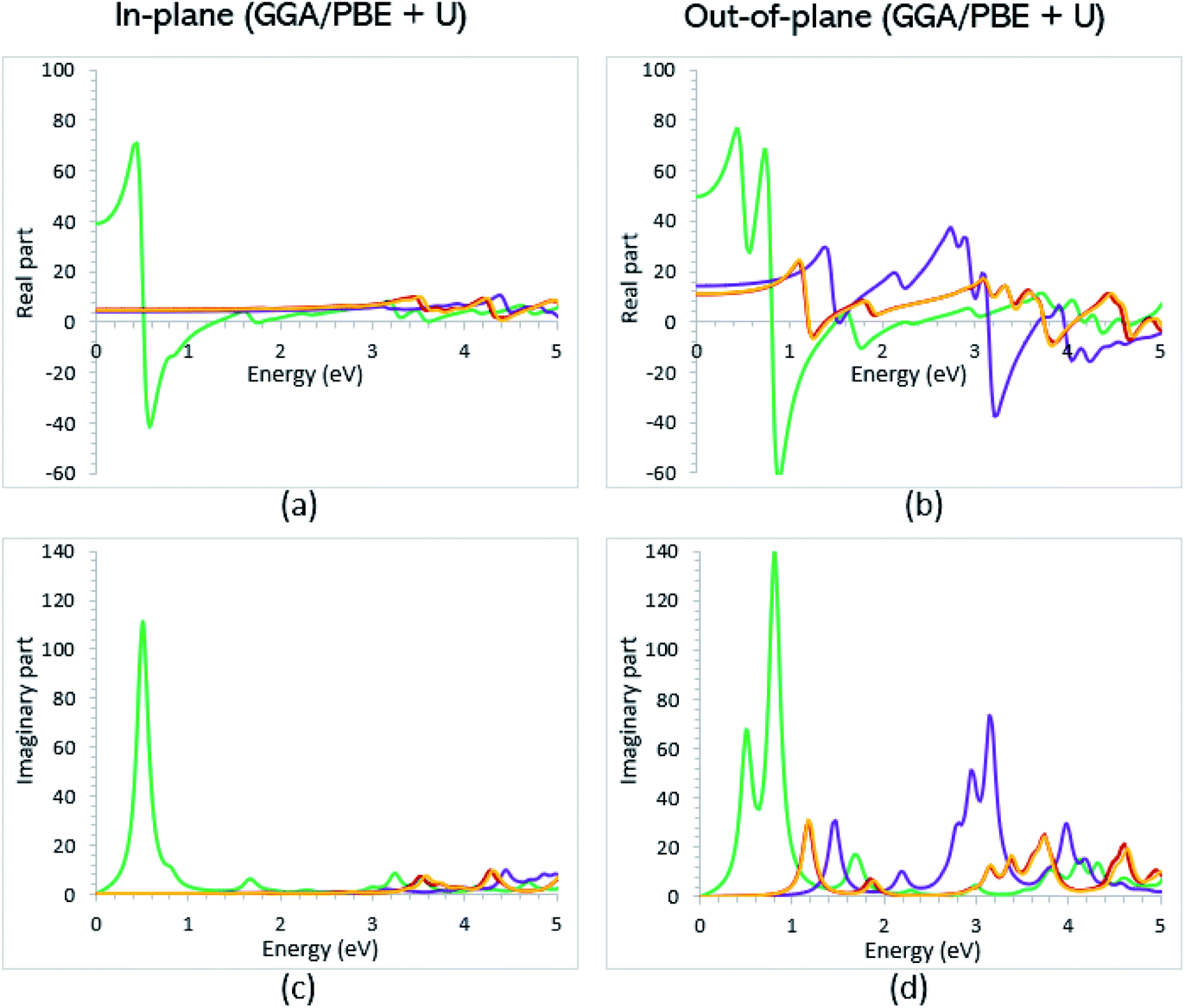
Once the electronic structure calculations confirmed the semiconducting character of the VO2(B) polymorph, we probed their optical properties for possible optoelectronics applications. The imaginary (ε2(ω)) and real parts (ε1(ω)) of the dielectric function, as well as the energy loss function for the VO2(B)PP, VO2(B)LP, VO2(B)PPD, and VO2(B)LPD structures are presented in Fig. 4–6 as functions of photon energy. We considered the parallel (in-plane) and perpendicular (out-of-plane) polarization directions within RPA + PBE and RPA + PBE + U. According to Fig. 4 and 5, the first main peak of ε2(ω) shows a weak absorption in the infrared range (1.24 meV to 1.7 eV) for the VO2(B)PP structure along the in-plane/out-of-plane polarizations. However, the situation changes remarkably for the VO2(B)LP, VO2(B)PPD, and VO2(B)LPD geometries, in which they indicate that the adsorption peaks in the infrared light are only along the out-of-plane polarizations. Based on the GGA/PBE calculations (Fig. 4), in the case of the in-plane polarization, only VO2(B)PP reveals a broad intense peak in the energy range of 0.47 eV, while all considered structures show peaks at 0.46, 1.06, 0.83 and 0.86 for the VO2(B)PP, VO2(B)LP, VO2(B)PPD, and VO2(B)LPD geometries, respectively, along the out-of-plane polarization direction. These peaks correspond to the transitions from π → π*. The next highly intense peaks in all geometries are related to the π → σ* transitions. We obtained the optical bandgap of 0.63, 0.56, and 0.60 eV for VO2(B)LP, VO2(B)PPD, and VO2(B)LPD, respectively, along the out-of-plane polarization direction. This is comparable (slightly smaller) to the bulk value of ∼0.6 eV.77 For the real part of the dielectric function related to the static dielectric function, it was found that the ε1(ω) part for VO2(B)PP, VO2(B)LP, VO2(B)PPD, and VO2(B)LPD geometries shows the positive values of 38.53, 4.60, 5.08 and 5.06 along the in-plane polarization, and 65.99, 19.50, 20.46 and 18.43 for the out-of-plane polarization directions, respectively. | ||
| Fig. 4 Imaginary and real parts of the dielectric function of VO2(B)PP (green), VO2(B)LP (purple), VO2(B)PPD (red), and VO2(B)LPD (orange) structures along the in-plane (a and c) and out-of-plane (b and d) polarizations, as predicted by RPA + PBE. | ||
From the predicted data based on the DFT + U calculations, as shown in Fig. 5, the adsorption peaks of ε2(ω) along the in-plane polarization show similar results to the PBE calculations. However, the peaks existing in the optical spectrum of the out-of-plane direction exhibit a blue shift in the light energy range of 1.43 eV for VO2(B)LP and an intense peak at 3.10 eV. By applying the U correction in the PBE calculations, the light polarization becomes more intense in VO2(B)PP, whereas the other three geometries exhibit the opposite behavior by decreasing the peak intensity. Moreover, our theoretical calculations indicate that the optical bandgaps of the VO2(B)PPD and VO2(B)LPD geometries slightly increase by ∼0.95 eV. Meanwhile, the optical bandgap of VO2(B)LP is situated at higher energies at 1.20 eV. A strange behavior is represented by the zero optical bandgap of VO2(B)PP at low photon energy. This distinct difference might occur because VO2(B)PP contains a longer V1–V2 = 3.33 Å (more weakly bonded) than the three other configurations with shorter V1–V2 bond distances of 2.81, 2.98 and 3.02 Å for VO2(B)LP, VO2(B)PPD, and VO2(B)LPD (Table 1), respectively. The amounts of static dielectric constants were calculated to be 39.32, 4.33, 4.86 and 4.83 along the in-plane direction, and 49.91, 14.55, 10.84 and 10.87 along the out-of-plane polarization direction, with a drop in comparison to the PBE functional. The static optical spectra with the positive value of both in-plane/out-of-plane dielectric constants are further proof of the VO2(B) conductivity. Lourembam et al.82 and Lee et al.80 experimentally confirmed the non-zero frequency of the real part of the optical conductivity of this polymorph.
 | ||
| Fig. 5 Imaginary and real parts of the dielectric function of VO2(B)PP (green), VO2(B)LP (purple), VO2(B)PPD (red), and VO2(B)LPD (orange) structures along the in-plane (a and c) and out-of-plane (b and d) polarizations, as predicted by RPA + PBE + U. | ||
As reported in the literature, the different experimental values of the static dielectric constant of VO2 have been observed. Yang et al.124 investigated the temperature dependence of the dielectric constant and carrier conduction in VO2 thin films. They outlined that the dielectric constant of VO2 can be increased from ∼36 at room temperature to a value exceeding 6 × 10⁴ at 100 °C. In another study, Hood et al.125 measured the dielectric constant of the VO2 structure across the phase transformation at 68 °C. In this work, the real part of the dielectric constant increased from less than 1000 to higher than 90![[thin space (1/6-em)]](https://www.rsc.org/images/entities/char_2009.gif) 000 by elongating the film thickness. Furthermore, the outcomes obtained by Mansingh et al.126 showed the approximated value of 100 for the static dielectric constant of VO2 single crystals in the frequency range of 30 to 105 Hz, and in the temperature range 77 to 250 K. From the theoretical side, Wan et al.83 used both experiment and first-principles PBE + U calculations to investigate the optical property of the VO2(B) structure. They observed the weak adsorption of this polymorph in the infrared light along the in-plane/out-of-plane polarization directions. According to the data presented in the literature for the other 2D oxides, VO2(B) possesses an excellent dielectric constant along the in-plane and out-of-plane directions. Its dielectric constant is higher than that for Al2O3 with a value of 8–10 and SiO2 with 3.9,127 and is comparable with that for HfO2 with a dielectric constant of 20–25.128 Our calculations indicate that VO2(B) can be a good replacement for SiO2 with a higher dielectric constant for application in field effect transistors (FETs) and capacitors of dynamic random-access memories. Meanwhile, the stronger infrared absorption of the VO2(B) polymorph is favorable for achieving the maximum sensitivity for the applications in uncooled infrared bolometer.129,130
000 by elongating the film thickness. Furthermore, the outcomes obtained by Mansingh et al.126 showed the approximated value of 100 for the static dielectric constant of VO2 single crystals in the frequency range of 30 to 105 Hz, and in the temperature range 77 to 250 K. From the theoretical side, Wan et al.83 used both experiment and first-principles PBE + U calculations to investigate the optical property of the VO2(B) structure. They observed the weak adsorption of this polymorph in the infrared light along the in-plane/out-of-plane polarization directions. According to the data presented in the literature for the other 2D oxides, VO2(B) possesses an excellent dielectric constant along the in-plane and out-of-plane directions. Its dielectric constant is higher than that for Al2O3 with a value of 8–10 and SiO2 with 3.9,127 and is comparable with that for HfO2 with a dielectric constant of 20–25.128 Our calculations indicate that VO2(B) can be a good replacement for SiO2 with a higher dielectric constant for application in field effect transistors (FETs) and capacitors of dynamic random-access memories. Meanwhile, the stronger infrared absorption of the VO2(B) polymorph is favorable for achieving the maximum sensitivity for the applications in uncooled infrared bolometer.129,130
The theoretical energy loss function computed by GGA/PBE and GGA/PBE + U is presented in Fig. 6(a)–(d). The energy-loss spectrum is important for describing the energy loss of electrons passing through the materials. While the spectrum calculated by GGA/PBE indicated broad peaks for the in-plane polarization in the energy range of 14–20 eV, GGA/PBE + U indicated in the high intensity peaks along the in-plane and out-of-plane polarization directions. The results reveal that the maximum energy loss peak value predicted by GGA/PBE for VO2(B)PP, VO2(B)LP, VO2(B)PPD and VO2(B)LPD reaches 19.26, 15.99, 16.09 and 16.09 eV along the in-plane polarization direction, and 14.45, 16.96, 15.96 and 15.96 eV for the out-of-plane polarization direction, respectively. The corresponding values predicted by the PBE + U functional are 19.06, 16.32, 16.62 and 15.55 eV along the in-plane polarization direction, and 14.45, 15.92, 16.02 and 16.02 eV along the out-of-plane polarization direction.
 | ||
| Fig. 6 Energy loss function spectra of VO2(B)PP (green), VO2(B)LP (purple), VO2(B)PPD (red), and VO2(B)LPD (orange) structures along the in-plane and out-of-plane polarizations, as predicted by RPA + PBE (a and b) and RPA + PBE + U (c and d). | ||
According to the theoretical study by Wan et al.,83 they found an electronic bandgap of 0.60 eV for the VO2(B) polymorph. However, the zero optical bandgap was observed in the ε2(ω) optical graph. This disagreement also occurred in our calculations, in which the VO2(B)PP structure showed an 0.76 eV electronic bandgap and zero optical bandgap. Conversely, VO2(B)PPD indicated a zero bandgap in the band structure calculations and a semiconductor optical property. On the other hand, VO2(B)LP was not able to support the correct optical bandgap when the U value was included in the PBE calculations. In conclusion, the subtle interplay between the electronic, magnetic, and optical properties leads to the VO2(B)PPD configuration describing the semiconductor electronic and optical bandgap well, and shows excellent agreement between experimental and theoretical observations. Therefore, on the basis of the DFT calculations with the PW approach and PBE-D3 method, this configuration strongly suggests a VO2(B) polymorph.
Conclusions
We have successfully reproduced the experimental electronic, magnetic and optical properties of the VO2(B) polymorph via DFT calculations. In this study, we optimized the geometry of the VO2(B) polymorph on the basis of the PW and LCAO approaches using the GGA/PBE functional and with exclusion/inclusion of the dispersion corrections. The analysis of the structural parameters showed the existence of four different geometries of VO2(B), namely VO2(B)PP, VO2(B)LP, VO2(B)PPD, and VO2(B)LPD obtained from different methods. In order to check for the reliability of the computational methods, particularly for the selected energy functional (PBE + U) with the Coulomb correlation effect, we calculated the electronic and optical bandgaps and magnetic state of the VO2(B) configurations for comparison with experiments. The electronic band structure and DOS revealed a zero bandgap for all considered geometries by using the conventional GGA/PBE approximation. However, applying a Hubbard U value of 5.20 eV for the V-3d orbitals significantly opened the bandgap up to 0.76, 0.66 eV and 0.70 eV for VO2(B)PP, VO2(B)LP and VO2(B)PPD, respectively. From these numerical calculations, we indicated that the DFT + U method can be used to change the gap size and induce a metal–semiconductor transition. PDOS solution was used in our potential energy scan and the magnetic properties were assessed. The PBE and PBE + U predicted the nonmagnetic state of the ground-state VO2(B) phase, which is consistent with the magnetic moment observed in experiments. Moreover, the optical properties including the imaginary and real parts of the dielectric function for the in-plane and out-of-plane polarizations for the VO2(B) geometries were evaluated. The first absorption peaks revealed that all considered geometries can perfectly absorb infrared light along the out-of-plane polarization. Notably, PBE and PBE + U confirmed its VO2(B) semiconducting feature with the static dielectric constants having positive values. The DFT-based verification of the nonmagnetic feature as well as the electronic and optical measurements of VO2(B)PPD, provide the important future research lines to physical characterization of other VO2 polymorphs.Author contributions
Conceptualization, E. M., E. L. and P. L. S.; methodology, E. M. and E. L.; validation, E. M., E. L. and P. L. S.; investigation, E. M.; data curation, E. M.; writing—original draft preparation, E. M.; writing—review and editing, E. M., E. L., E. P. and P. L. S.; visualization, E. M.; supervision, P. L. S.; project administration, E. M., E. L., P. L. S., L. P. and D. M. All authors have read and agreed to the published version of the manuscript.Conflicts of interest
There are no conflicts to declare.Acknowledgements
This work is part of the research of H2020 (FETPROACT-EIC-05-2019) “Nanomaterials enabling smart energy harvesting for next-generation Internet-of-Things” (NANO-EH) (grant agreement No. 951761). We would also like to thank CINECA-HPC ISCRA MARCONI-100 computer system (NANO-PR project n. HP10CK3EZ0) for the calculations on QE.References
- C. N. R. Rao, Annu. Rev. Phys. Chem., 1989, 40, 326 CrossRef.
- S. Lany, J. Phys.: Condens. Matter, 2015, 27, 283203 CrossRef PubMed.
- S. Maekawa, T. Tohyama, S. E. Barnes, S. Ishihara, W. Koshibae and G. Khaliullin, Physics of Transition Metal Oxides, Springer Science & Business Media, 2004 Search PubMed.
- P. Lunkenheimer, S. Krohns, S. Riegg, S. G. Ebbinghaus, A. Reller and A. Loidl, Eur. Phys. J.: Spec. Top., 2009, 180, 89 Search PubMed.
- A. Laturia, M. L. Van de Put and W. G. Vandenberghe, npj 2D Mater. Appl., 2018, 2, 7 CrossRef.
- S. Walia, S. Balendhran, H. Nili, S. Zhuiykov, G. Rosengarten, Q. H. Wang, M. Bhaskaran, S. Sriram, M. S. Strano and K. Kalantar-zadeh, Prog. Mater. Sci., 2013, 58, 1489 CrossRef.
- S. Ghosh, S. Harish, M. Ohtaki and B. B. Saha, Mater. Today Energy, 2020, 18, 100492 CrossRef CAS.
- G. Özbal, R. T. Senger, C. Sevik and H. Sevinçli, Phys. Rev. B, 2019, 100, 085415 CrossRef.
- J. Haber, Catalysis by Transition Metal Oxides, 1985 Search PubMed.
- W. T. Hong, M. Risch, K. A. Stoerzinger, A. Grimaud, J. Suntivich and Y. Shao-Horn, Energy Environ. Sci., 2015, 8, 1427 Search PubMed.
- I. Yamada, A. Takamatsu, K. Asai, H. Ohzuku, T. Shirakawa, T. Uchimura, S. Kawaguchi, H. Tsukasaki, S. Mori, K. Wada and H. Ikeno, ACS Appl. Energy Mater., 2018, 1, 3721 Search PubMed.
- J. H. Linn and W. E. Swartz Jr, Appl. Surf. Sci., 1984, 20, 166 CrossRef.
- G. Lucovsky, Y. Zhang, G. B. Rayner Jr, G. Appel, H. Ade and J. L. Whitten, J. Vac. Sci. Technol., B: Microelectron. Nanometer Struct.--Process., Meas., Phenom., 2002, 20, 1747 Search PubMed.
- J. Y. Kwon and J. K. Jeong, Semicond. Sci. Technol., 2015, 30, 024002 CrossRef CAS.
- H. J. Lee, S. Lee, Y. Ji, K. G. Cho, K. S. Choi, C. Jeon, K. H. Lee and K. Hong, ACS Appl. Mater. Interfaces, 2019, 11, 40251 Search PubMed.
- H. Moon, D. Im and S. Yoo, IEEE Electron Device Lett., 2013, 34, 1016 Search PubMed.
- S. Kim, A. Konar, W. S. Hwang, J. H. Lee, J. Lee, J. Yang, C. Jung, H. Kim, J. B. Yoo, J. Y. Choi and Y. W. Jin, Nat. Commun., 2012, 3, 7 Search PubMed.
- Y. S. Shiah, K. Sim, Y. Shi, K. Abe, S. Ueda, M. Sasase and H. Hosono, Nat. Electron., 2021, 4, 807 Search PubMed.
- Z. Liang, L. Zhao, W. Meng, C. Zhong, S. Wei, B. Dong, Z. Xu, L. Wan and S. Wang, J. Alloys Compd., 2017, 694, 131 Search PubMed.
- M. Y. Hassaan, H. M. Osman, H. H. Hassan, A. S. El-Deeb and M. A. Helal, Ceram. Int., 2017, 43, 1801 CrossRef.
- S. Chen, Z. Wang, H. Ren, Y. Chen, W. Yan, C. Wang, B. Li, J. Jiang and C. Zou, Sci. Adv., 2019, 5, eaav6815 CrossRef CAS PubMed.
- K. I. Shimizu, I. Chinzei, H. Nishiyama, S. Kakimoto, S. Sugaya, W. Matsutani and A. Satsuma, Sens. Actuators, B, 2009, 141, 416 CrossRef.
- V. Mounasamy, G. K. Mani and S. Madanagurusamy, Microchim. Acta, 2020, 187, 29 CrossRef PubMed.
- J. Liang, J. Liu, N. Li and W. Li, J. Alloys Compd., 2016, 671, 290 CrossRef.
- S. Iqbal, L. T. Duy, H. Kang, R. Singh, M. Kumar, J. Park and H. Seo, Adv. Funct. Mater., 2021, 31, 2102567 CrossRef CAS.
- C. Y. Lin, Y. T. Tseng, P. H. Chen, T. C. Chang, J. K. Eshraghian, Q. Wang, Q. Lin, Y. F. Tan, M. C. Tai, W. C. Hung and H. C. Huang, Appl. Mater. Today, 2020, 21, 100848 CrossRef.
- Y. Ke, S. Wang, G. Liu, M. Li, T. J. White and Y. Long, Small, 2018, 14, 1802025 CrossRef PubMed.
- F. W. Yang, K. H. Chen, C. M. Cheng and F. Y. Su, Ceram. Int., 2013, 39, S732 Search PubMed.
- A. Velichko, A. Pergament, V. Putrolaynen, O. Berezina and G. Stefanovich, Mater. Sci. Semicond. Process., 2015, 29, 320 CrossRef.
- J. G. Ramirez, T. Saerbeck, S. Wang, J. Trastoy, M. Malnou, J. Lesueur, J. P. Crocombette, J. E. Villegas and I. K. Schuller, Phys. Rev. B: Condens. Matter Mater. Phys., 2015, 91, 205123 CrossRef.
- C. Ko, Z. Yang and S. Ramanathan, ACS Appl. Mater. Interfaces, 2011, 3, 3401 Search PubMed.
- S. Hormoz and S. Ramanathan, Solid-State Electron., 2010, 54, 659 CrossRef.
- N. F. Quackenbush, J. W. Tashman, J. A. Mundy, S. Sallis, H. Paik, R. Misra, J. A. Moyer, J. H. Guo, D. A. Fischer, J. C. Woicik and D. A. Muller, Nano Lett., 2013, 13, 4861 CrossRef PubMed.
- A. Sharoni, J. G. Ramírez and I. K. Schuller, Phys. Rev. Lett., 2008, 101, 026404 CrossRef PubMed.
- D. Ruzmetov, S. D. Senanayake, V. Narayanamurti and S. Ramanathan, Phys. Rev. B: Condens. Matter Mater. Phys., 2008, 77, 195442 CrossRef.
- A. N. Hattori, A. I. Osaka, K. Hattori, Y. Naitoh, H. Shima, H. Akinaga and H. Tanaka, Crystals, 2020, 10, 631 CrossRef CAS.
- J. Lappalainen, S. Heinilehto, H. Jantunen and V. Lantto, J. Electroceram., 2009, 22, 77 CrossRef.
- T. Huang, L. Yang, J. Qin, F. Huang, X. Zhu, P. Zhou, B. Peng, H. Duan, L. Deng and L. Bi, Opt. Mater. Express, 2016, 6, 3621 Search PubMed.
- A. Crunteanu, M. Fabert, J. Cornette, M. Colas, J. C. Orlianges, A. Bessaudou and F. Cosset, in Oxide-based Materials and Devices VI, 2015, vol. 9364, p. 52 Search PubMed.
- A. Crunteanu, J. Givernaud, J. Leroy, D. Mardivirin, C. Champeaux, J. C. Orlianges, A. Catherinot and P. Blondy, Sci. Technol. Adv. Mater., 2010, 11, 1–6 CrossRef PubMed.
- W. Xue, G. Liu, Z. Zhong, Y. Dai, J. Shang, Y. Liu, H. Yang, X. Yi, H. Tan, L. Pan and S. Gao, Adv. Mater., 2017, 29, 1702162 CrossRef PubMed.
- D. Wickramaratne, N. Bernstein and I. I. Mazin, Phys. Rev. B, 2019, 99, 214103 CrossRef CAS.
- J. Jeong, N. Aetukuri, T. Graf, T. D. Schladt, M. G. Samant and S. S. Parkin, Science, 2013, 339, 1405 CrossRef PubMed.
- K. Martens, I. P. Radu, S. Mertens, X. Shi, L. Nyns, S. Cosemans, P. Favia, H. Bender, T. Conard, M. Schaekers and S. De Gendt, J. Appl. Phys., 2012, 112, 124501 CrossRef.
- E. Strelcov, Y. Lilach and A. Kolmakov, Nano Lett., 2009, 9, 2326 CrossRef PubMed.
- Z. Hiroi, Prog. Solid State Chem., 2015, 43, 69 CrossRef.
- Q. Lu, S. R. Bishop, D. Lee, S. Lee, H. Bluhm, H. L. Tuller, H. N. Lee and B. Yildiz, Adv. Funct. Mater., 2018, 28, 1803024 CrossRef.
- K. Schneider and W. Maziarz, Sensors, 2018, 18, 4177 CrossRef PubMed.
- F. Pfuner, J. Schoiswohl, M. Sock, S. Surnev, M. G. Ramsey and F. P. Netzer, J. Phys.: Condens. Matter, 2005, 17, 4035 CrossRef CAS.
- B. Qi, H. P. Gunnlaugsson, S. Ólafsson, H. P. Gislason, E. B. Thorsteinsson, U. B. Arnalds, R. Mantovan, I. Unzueta, D. V. Zyabkin, K. B. Ram and K. Johnston, Thin Solid Films, 2020, 714, 138389 CrossRef CAS.
- A. K. Kundu, S. Barman and K. S. Menon, ACS Appl. Mater. Interfaces, 2021, 13, 20787 Search PubMed.
- B. Fisher, L. Patlagan, K. B. Chashka, C. Makarov and G. M. Reisner, Appl. Phys. Lett., 2016, 109, 103501 CrossRef.
- M. Marezio, P. D. Dernier, D. B. McWhan and J. P. Remeika, Mater. Res. Bull., 1970, 5, 1023 CrossRef.
- S. Suga, A. Sekiyama, M. Obara, J. Yamaguchi, M. Kimura, H. Fujiwara, A. Irizawa, K. Yoshimura, M. Yabashi, K. Tamasaku and A. Higashiya, J. Phys. Soc. Jpn., 2010, 79, 044713 CrossRef.
- T. Toriyama, T. Nakayama, T. Konishi and Y. Ohta, Phys. Rev. B: Condens. Matter Mater. Phys., 2014, 90, 085131 CrossRef CAS.
- (a) J. M. Longo, P. Kierkegaard, C. J. Ballhausen, U. Ragnarsson, S. E. Rasmussen, E. Sunde and N. A. Sørensen, Acta Chem. Scand., 1970, 24, 426 CrossRef; (b) S. Ji, Y. Zhao, F. Zhang and P. Jin, J. Cryst. Growth, 2010, 312, 286 CrossRef.
- F. J. Morin, Phys. Rev. Lett., 1959, 3, 34 CrossRef CAS.
- T. Mitsuishi, Jpn. J. Appl. Phys., 1967, 6, 1060 CrossRef CAS.
- Y. Oka, T. Yao and N. Yamamoto, J. Solid State Chem., 1990, 86, 124 CrossRef.
- F. Théobald, R. Cabala and J. Bernard, J. Solid State Chem., 1976, 17, 438 CrossRef.
- C. Wu, Z. Hu, W. Wang, M. Zhang, J. Yang and Y. Xie, Chem. Commun., 2008, 33, 3893 Search PubMed.
- Y. Wang, Z. Zhang, Y. Zhu, Z. Li, R. Vajtai, L. Ci and P. M. Ajayan, ACS Nano, 2008, 2, 1496 Search PubMed.
- A. M. N. F. Zylbersztejn and N. F. Mott, Phys. Rev. B: Solid State, 1975, 11, 4383 CrossRef CAS.
- J. Lourembam, A. Srivastava, C. La-o-Vorakiat, L. Cheng, T. Venkatesan and E. E. Chia, Sci. Rep., 2016, 6, 7 CrossRef PubMed.
- J. Zhang and R. D. Averitt, Annu. Rev. Mater. Res., 2014, 44, 43 CrossRef.
- J. Zhou, Y. Gao, Z. Zhang, H. Luo, C. Cao, Z. Chen, L. Dai and X. Liu, Sci. Rep., 2013, 3, 5 Search PubMed.
- M. M. Qazilbash, M. Brehm, G. O. Andreev, A. Frenzel, P. C. Ho, B. G. Chae, B. J. Kim, S. J. Yun, H. T. Kim, A. V. Balatsky and O. G. Shpyrko, Phys. Rev. B: Condens. Matter Mater. Phys., 2009, 79, 075107 CrossRef.
- S. H. Chang, S. B. Lee, D. Y. Jeon, S. J. Park, G. T. Kim, S. M. Yang, S. C. Chae, H. K. Yoo, B. S. Kang, M. J. Lee and T. W. Noh, Adv. Mater., 2011, 23, 4067 Search PubMed.
- M. Nakano, K. Shibuya, D. Okuyama, T. Hatano, S. Ono, M. Kawasaki, Y. Iwasa and Y. Tokura, Nature, 2012, 487, 462 CrossRef PubMed.
- M. S. Kang, S. K. Park, P. Nakhanivej, K. H. Shin, J. S. Yeon and H. S. Park, J. Alloys Compd., 2021, 855, 157361 CrossRef CAS.
- N. Ganganagappa and A. Siddaramanna, Mater. Charact., 2012, 68, 62 CrossRef.
- Q. Wang, J. Pan, M. Li, Y. Luo, H. Wu, L. Zhong and G. Li, J. Mater. Sci. Technol., 2015, 31, 633 Search PubMed.
- Y. Liu, E. Uchaker, N. Zhou, J. Li, Q. Zhang and G. Cao, J. Mater. Chem., 2012, 22, 24445 Search PubMed.
- S. Zhang, B. Shang, J. Yang, W. Yan, S. Wei and Y. Xie, Phys. Chem. Chem. Phys., 2011, 13, 15881 Search PubMed.
- Y. Zhang, Mater. Sci., 2016, 34, 176 Search PubMed.
- A. Cavalleri, M. Rini, H. H. W. Chong, S. Fourmaux, T. E. Glover, P. A. Heimann, J. C. Kieffer and R. W. Schoenlein, Phys. Rev. Lett., 2005, 95, 067405 CrossRef CAS PubMed.
- (a) M. M. Qazilbash, M. Brehm, B. G. Chae, P. C. Ho, G. O. Andreev, B. J. Kim, S. J. Yun, A. V. Balatsky, M. B. Maple, F. Keilmann and H. T. Kim, Science, 2007, 318, 1753 CrossRef PubMed; (b) T. L. Cocker, L. V. Titova, S. Fourmaux, G. Holloway, H. C. Bandulet, D. Brassard, J. C. Kieffer, M. A. El Khakani and F. A. Hegmann, Phys. Rev. B: Condens. Matter Mater. Phys., 2012, 85, 155120 CrossRef.
- C. N. Berglund and H. J. Guggenheim, Phys. Rev., 1969, 185, 1022 CrossRef CAS.
- https://materialsproject.org/materials/mp-561637/ .
- S. Lee, T. L. Meyer, C. Sohn, D. Lee, J. Nichols, D. Lee, S. S. A. Seo, J. W. Freeland, T. W. Noh and H. N. Lee, APL Mater., 2015, 3, 126109 CrossRef.
- S. R. Popuri, A. Artemenko, R. Decourt, M. Josse, U. C. Chung, D. Michau, M. Maglione, A. Villesuzanne and M. Pollet, J. Phys. Chem. C, 2015, 119, 25085–25092 CrossRef CAS.
- J. Lourembam, A. Srivastava, C. La-o-vorakiat, H. Rotella, T. Venkatesan and E. E. Chia, Sci. Rep., 2015, 5, 8 Search PubMed.
- D. Wan, P. Xiong, L. Chen, S. Shi, A. Ishaq, H. Luo and Y. Gao, Appl. Surf. Sci., 2017, 397, 39 CrossRef.
- C. Xia, Z. Lin, Y. Zhou, C. Zhao, H. Liang, P. Rozier, Z. Wang and H. N. Alshareef, Adv. Mater., 2018, 30, 1803594 CrossRef PubMed.
- Y. Oka, T. Yao, N. Yamamoto, Y. Ueda and A. Hayashi, J. Solid State Chem., 1993, 105, 278 CrossRef.
- S. R. Popuri, M. Miclau, A. Artemenko, C. Labrugere, A. Villesuzanne and M. Pollet, Inorg. Chem., 2013, 52, 4785 CrossRef PubMed.
- A. Srivastava, H. Rotella, S. Saha, B. Pal, G. Kalon, S. Mathew, M. Motapothula, M. Dykas, P. Yang, E. Okunishi and D. D. Sarma, APL Mater., 2015, 3, 026101 CrossRef.
- C. W. Huang, S. S. Kuo and C. L. Hsin, CrystEngComm, 2018, 20, 6860 Search PubMed.
- C. Kim, Y. Oikawa, J. S. Shin and H. Ozaki, J. Phys.: Condens. Matter, 2006, 18, 9863 CrossRef CAS.
- E. Laudadio, P. Stipa, L. Pierantoni and D. Mencarelli, Crystals, 2022, 12, 90 CrossRef CAS.
- P. Giannozzi, O. Andreussi, T. Brumme, O. Bunau, M. B. Nardelli, M. Calandra, R. Car, C. Cavazzoni, D. Ceresoli, M. Cococcioni and N. Colonna, J. Phys.: Condens. Matter, 2017, 29, 465901 CrossRef CAS PubMed.
- S. Smidstrup, T. Markussen, P. Vancraeyveld, J. Wellendorff, J. Schneider, T. Gunst, B. Verstichel, D. Stradi, P. A. Khomyakov, U. G. Vej-Hansen and M. E. Lee, J. Phys.: Condens. Matter, 2019, 32, 015901 CrossRef PubMed.
- P. Hohenberg and W. Kohn, Phys. Rev., 1964, 136, B864 CrossRef.
- W. Kohn and L. J. Sham, Phys. Rev., 1965, 140, A1133 CrossRef.
- M. J. van Setten, M. Giantomassi, E. Bousquet, M. J. Verstraete, D. R. Hamann, X. Gonze and G. M. Rignanese, Comput. Phys. Commun., 2018, 226, 54 CrossRef.
- P. E. Blöchl, Phys. Rev. B: Condens. Matter Mater. Phys., 1994, 50, 17953 CrossRef PubMed.
- J. P. Perdew, K. Burke and M. Ernzerhof, Phys. Rev. Lett., 1996, 77, 3865 CrossRef CAS PubMed.
- L. Brillouin, C. R. Hebd. Seances Acad. Sci., 1930, 191, 292 CAS.
- D. Vanderbilt, Phys. Rev. B: Condens. Matter Mater. Phys., 1990, 41, 7892 CrossRef PubMed.
- S. Grimme, S. Ehrlich and L. Goerigk, J. Comput. Chem., 2011, 32, 1465 CrossRef PubMed.
- D. C. Liu and J. Nocedal, Math. Program., 1989, 45, 528 CrossRef.
- J. Hubbard, Proc. R. Soc. London, Ser. A, 1964, 281, 419 Search PubMed.
- J. Hubbard, Proc. R. Soc. London, Ser. A, 1964, 277, 259 Search PubMed.
- T. J. Huffman, P. Xu, M. M. Qazilbash, E. J. Walter, H. Krakauer, J. Wei, D. H. Cobden, H. A. Bechtel, M. C. Martin, G. L. Carr and D. N. Basov, Phys. Rev. B: Condens. Matter Mater. Phys., 2013, 87, 115121 CrossRef.
- O. V. Sedelnikova, L. G. Bulusheva and A. V. Okotrub, J. Chem. Phys., 2011, 134, 244707 CrossRef CAS PubMed.
- L. Yang, J. Deslippe, C. H. Park, M. L. Cohen and S. G. Louie, Phys. Rev. Lett., 2009, 103, 186802 CrossRef PubMed.
- F. Wooten, Am. J. Phys., 1973, 41, 939–940 CrossRef.
- B. Mortazavi, M. Shahrokhi, M. Makaremi and T. Rabczuk, Nanotechnology, 2017, 28, 115705 CrossRef PubMed.
- B. Mortazavi, M. Shahrokhi, A. V. Shapeev, T. Rabczuk and X. Zhuang, J. Mater. Chem. C, 2019, 7, 10917 Search PubMed.
- K. Kolwas and A. Derkachova, Nanomaterials, 2020, 10, 1411 CrossRef CAS PubMed.
- R. F. Egerton, Electron Energy-Loss Spectroscopy in the Electron Microscope, Springer Science & Business Media, 2011 Search PubMed.
- Z. Xie, L. Hui, J. Wang, Z. Chen and C. Li, Comput. Mater. Sci., 2018, 144, 314 CrossRef.
- A. Kokalj, J. Mol. Graphics Modell., 1999, 17, 179 CrossRef.
- J. P. Perdew and M. Levy, Phys. Rev. Lett., 1983, 51, 1884 CrossRef CAS.
- A. Liebsch, H. Ishida and G. Bihlmayer, Phys. Rev. B: Condens. Matter Mater. Phys., 2005, 71, 085109 CrossRef.
- D. Gao, J. Dong, R. Xiao, B. Shang, D. Yu, C. Chen, Y. Liu, K. Zheng and F. Pan, Phys. Chem. Chem. Phys., 2022, 24, 2150–2157 RSC.
- S. Chen, J. Liu, H. Luo and Y. Gao, J. Phys. Chem. Lett., 2015, 6, 3656 Search PubMed.
- S. Chen, J. Liu, L. Wang, H. Luo and Y. Gao, J. Phys. Chem. C, 2014, 118, 18944 Search PubMed.
- R. M. Olson, A. V. Marenich, C. J. Cramer and D. G. Truhlar, J. Chem. Theory Comput., 2007, 3, 2054 Search PubMed.
- J. Li, T. Zhu, C. J. Cramer and D. G. Truhlar, J. Phys. Chem. A, 1998, 102, 1831 Search PubMed.
- D. Guo, C. Hu, Q. Yang, H. Hua, W. Li and C. Kong, Mater. Res. Bull., 2014, 53, 106 CrossRef.
- D. Guo, C. Hu, Z. Zhao, Y. Xi and H. Liu, Sci. Adv. Mater., 2014, 6, 282 Search PubMed.
- J. Liu, Q. Li, T. Wang, D. Yu and Y. Li, Angew. Chem., 2004, 116, 5162 CrossRef.
- Z. Yang, C. Ko, V. Balakrishnan, G. Gopalakrishnan and S. Ramanathan, Phys. Rev. B: Condens. Matter Mater. Phys., 2010, 82, 205101 CrossRef.
- P. J. Hood and J. F. DeNatale, J. Appl. Phys., 1991, 70, 381 CrossRef.
- A. Mansingh, R. Singh and M. Sayer, Phys. Status Solidi A, 1978, 49, 779 CrossRef.
- J. Robertson, Eur. Phys. J.: Appl. Phys., 2004, 28, 291 CrossRef.
- J. T. Gaskins, P. E. Hopkins, D. R. Merrill, S. R. Bauers, E. Hadland, D. C. Johnson, D. Koh, J. H. Yum, S. Banerjee, B. J. Nordell and M. M. Paquette, ECS J. Solid State Sci. Technol., 2017, 6, N189 CrossRef CAS.
- B. Guo, D. Wan, A. Ishaq, H. Luo and Y. Gao, J. Alloys Compd., 2017, 715, 136 CrossRef.
- T. H. Kil, H. J. Choi, G. Lee, B. H. Lee, S. Y. Jung, R. Ning, C. Park, S. O. Won, H. J. Chang, W. J. Choi and S. H. Baek, J. Eur. Ceram. Soc., 2020, 40, 5588 CrossRef.
| This journal is © The Royal Society of Chemistry 2022 |