
 Open Access Article
 This Open Access Article is licensed under a Creative Commons Attribution-Non Commercial 3.0 Unported Licence
Low temperature 2D GaN growth on Si(111) 7 × 7 assisted by hyperthermal nitrogen ions†
Jaroslav
Maniš
ab,
Jindřich
Mach
 *ab,
Miroslav
Bartošík
abc,
Tomáš
Šamořil
b,
Michal
Horák
b,
Vojtěch
Čalkovský
b,
David
Nezval
b,
Lukáš
Kachtik
a,
Martin
Konečný
ab and
Tomáš
Šikola
ab
*ab,
Miroslav
Bartošík
abc,
Tomáš
Šamořil
b,
Michal
Horák
b,
Vojtěch
Čalkovský
b,
David
Nezval
b,
Lukáš
Kachtik
a,
Martin
Konečný
ab and
Tomáš
Šikola
ab
aCEITEC BUT, Brno University of Technology, Technická 3058/10, 616 00 Brno, Czech Republic. E-mail: mach@fme.vutbr.cz
bInstitute of Physical Engineering, Brno University of Technology, Technická 2, 616 69 Brno, Czech Republic
cDepartment of Physics and Materials Engineering, Faculty of Technology, Tomas Bata University in Zlín, Vavrečkova 275, 760 01, Czech Republic
First published on 19th July 2022
Abstract
As the characteristic dimensions of modern top-down devices are getting smaller, such devices reach their operational limits imposed by quantum mechanics. Thus, two-dimensional (2D) structures appear to be one of the best solutions to meet the ultimate challenges of modern optoelectronic and spintronic applications. The representative of III–V semiconductors, gallium nitride (GaN), is a great candidate for UV and high-power applications at a nanoscale level. We propose a new way of fabrication of 2D GaN on the Si(111) 7 × 7 surface using post-nitridation of Ga droplets by hyperthermal (E = 50 eV) nitrogen ions at low substrate temperatures (T < 220 °C). The deposition of Ga droplets and their post-nitridation are carried out using an effusion cell and a special atom/ion beam source developed by our group, respectively. This low-temperature droplet epitaxy (LTDE) approach provides well-defined ultra-high vacuum growth conditions during the whole fabrication process resulting in unique 2D GaN nanostructures. A sharp interface between the GaN nanostructures and the silicon substrate together with a suitable elemental composition of nanostructures was confirmed by TEM. In addition, SEM, X-ray photoelectron spectroscopy (XPS), AFM and Auger microanalysis were successful in enabling a detailed characterization of the fabricated GaN nanostructures.
1. Introduction
Motivated by the discovery of graphene, scientists have made a great effort to extend their knowledge and fabricate other two-dimensional (2D) materials. Among others, 2D forms of III–V semiconductor nanostructures, such as gallium nitride (GaN) layers, represent a suitable material for optical applications. GaN based ultraviolet laser diodes are used for water cleaning1 or gas detoxification,2–4 or as a light source for optical disc recording technologies. The very high breakdown voltage and high electron mobility also make it an ideal material for high-performance, high-frequency devices (for example, for high-speed wireless data transmission and high-voltage switching).In addition, 2D semiconductors are one of the potential candidates for overcoming the short-channel effects (mitigating heat dissipation) in FETs,5,6 which could improve the efficiency of these devices greatly. Recently, an excellent storage capacity has been reported when 2D GaN was used as an anode in Li-ion and Na-ion batteries.7 The ferromagnetic properties of 2D GaN have been studied from the perspective of doping with copper8 and other elements,9 showing large spin polarization and high Curie temperature. The role of vacancies in electrical properties10 and the impact of buckling of a 2D GaN structure on carrier mobility11 have already been investigated with promising results, thus paving the way for implementing 2D GaN nanostructures in spintronic nanodevices.
The first successful attempt to fabricate two-dimensional gallium nitride was achieved by a migration enhanced epitaxial growth (MEEG) method.12 2D GaN was grown sandwiched in between graphene and a passivated silicon substrate. The authors suggested that graphene plays a crucial role in stabilizing the direct 5 eV GaN bandgap. The MEEG technique also allows us to control the growth rate of the 2D GaN structure resulting in the precise control of the number of formed layers. It has been shown that the number of layers has a crucial role in controlling the crystallographic structure which further influences the band gap of the GaN structure.13 Even though the MEEG method enables the growth of 2D GaN, the sandwiched structure limits further applications since it hinders the possibility of transferring the fabricated nanostructure to other materials.
Recently, researchers have developed a method for fabrication of micrometer-sized 2D GaN structures of maximum thickness.14 Heat decomposition of a nitrogen precursor and subsequent reaction of nitrogen with liquefied gallium spread over a tungsten substrate leads to the formation of a uniform 2D GaN layer. The reported 2D GaN exhibits promising electrical and optical properties along with the possibility of transferring the structure to other materials as demonstrated by a fabricated functional device.
However, all referenced 2D nanostructures were fabricated by MOCVD methods which have several disadvantages. Firstly, high temperatures and hazardous precursors which are inflammable and poisonous have been generally used. Secondly, impurities can be introduced into the formed nanostructure during the growth process due to a higher operational and base pressure which usually reaches tens and hundreds of pascals, respectively. Since impurities generally affect the electronic and optical properties significantly (e.g. as dopants), it is highly demanding to find fabrication techniques that enable the reduction of additional elements significantly. In addition, the MOCVD technique is not suitable for real-time in situ surface analysis of grown nanostructures.
Droplet epitaxy (DE) is an alternative fabrication method of nanostructures which can be carried out in standard MBE vacuum chambers.15,16 Even though DE was originally developed for the fabrication of GaAs nanodots,17 in this paper we show how to adopt this method for growth of GaN nanostructures. The DE method offers the advantage of precise control of the ambient environment since it introduces only the elements of interest and allows us to conduct the fabrication process under ultra-high vacuum (UHV) conditions. On top of that, the precise control of the deposition rate enables us to achieve the required nanostructure size. We propose to adopt DE for low-temperature synthesis of GaN by using a special ion/atom beam source developed by our group and capable of working under UHV conditions.18,19 In this way, a low-temperature droplet epitaxy (LTDE) method under the well-defined conditions was utilized for fabrication of planar GaN triangular nanocrystals with a crystal structure different from that of wurtzite GaN and qualitatively and quantitatively corresponding to that of 2D GaN nanocrystals. Such a low-temperature growth opens the way for fabrication of photoactive 2D GaN nanostructures in the vicinity of already pre-fabricated metallic plasmonic antennas, thus enabling optimization of plasmon-enhanced photoluminescence effects and other plasmon-based phenomena (e.g. strong coupling).
2. Experimental section
2D GaN nanostructures were fabricated by a hybrid method alternating deposition of Ga atoms and ultra-low energy (hyperthermal) nitrogen ions (E = 50 eV) at low substrate temperature. An n-doped Si(111) single crystal (resistivity ρ = 0.01–0.02 Ω cm) with 0.2° and 4° miscut angles was used as a substrate. After insertion into a UHV chamber, the silicon substrate was annealed at 700 °C (measured by a pyrometer) for at least 12 hours by direct current heating. Afterwards, a flashing routine, i.e. a periodic rapid increase and decrease of temperature up to 1250 °C and down to 800 °C, respectively, followed by a slow temperature decrease to room temperature (RT) was carried out. Simultaneously, the pressure during the whole procedure was kept below 1 × 10⁻⁶ Pa. The flashing routine provides two benefits – complete decomposition of a native silicon oxide layer and formation of the 7 × 7 surface Si reconstruction. The substrate prepared by this procedure exhibited high surface cleanliness confirmed by XPS, and a uniform surface with large terraces determined by LEED.Gallium atoms were deposited by an effusion cell in a UHV chamber at a base pressure of 5 × 10⁻⁸ Pa and a substrate temperature of 330 °C using a flux rate of 7 × 10¹² atoms per cm2 per s which resulted in a substrate coverage of 4 × 10¹⁶ atoms per cm2 (5 monolayers).
Nitridation of gallium droplets was then carried out by hyperthermal nitrogen ions (E = 50 eV) at a substrate temperature of 190–210 °C using the ion/atom beam nitrogen source (ion-beam source mode only) at a nitrogen partial pressure of 5.5 × 10⁻⁵ Pa. During nitridation, the flux of nitrogen ions (N+ and N2+) provided a current density of 1000 nA cm−2 at a beam incidence angle of 55°.
The morphology of 2D GaN nanostructures was studied ex situ by scanning electron microscopy (SEM – Verios 360L system, Thermo Fisher Scientific) and atomic force microscopy (AFM – ICON, Bruker). The structural microanalysis was conducted in a complex vacuum system dedicated for scanning Auger microscopy (NanoSAM equipped with a UHV Gemini electron column). A TEM lamella for investigation of the crystallographic structure was prepared using a focused Ga ion beam system (FIB) in a SEM system (Lyra, Tescan) and the crystallographic and EDS studies were performed in a TEM/STEM system (Titan, Thermo Fisher Scientific). The values and error intervals of lattice parameters were obtained by a statistical processing (standard deviations) of periodicities in the real space high-resolution image. XPS was carried out using an experimental setup consisting of an X-ray source (DAR400) and a hemispherical electrostatic analyzer (both Omicron).
3. Results and discussion
The fabrication of 2D GaN nanostructures using the droplet epitaxy method is a two-step process. Firstly, the deposition of metallic gallium results in the formation of gallium droplets uniformly spread over the Si(111) 7 × 7 surface. Secondly, subsequent nitridation leads to a transformation of Ga droplets into GaN nanocrystals. This process is described in detail in ref. 20 and also in our paper.21 The size and density of Ga droplets on the Si(111) 7 × 7 surface can be controlled both by the surface temperature and deposition time.22 Ga deposition on Si(111) 7 × 7 was carried out for 50 min (resulting in a coverage of 5 ML) at 330 °C. The density of gallium droplets spread over the Si(111) 7 × 7 surface was approximately 3 × 10⁸ droplets per cm2. For these deposition conditions a droplet diameter of 200 nm and height of 70 nm have been observed by AFM. Afterwards, the substrate temperature was decreased to 210 °C and gallium droplets were exposed to a hyperthermal nitrogen ion beam (E = 50 eV) for 120 min to accomplish post-nitridation. The temperature during the post-nitridation process was the critical parameter of the experiment since the growth of 2D GaN was observed only in a narrow low temperature window of 190–210 °C. While at 180 °C there was an onset of droplet epitaxy growth, at 220 °C small 3D GaN nanocrystallites had started to protrude from a gallium droplet surface (see Fig. S2 in the ESI†).Fig. 1a shows a SEM image of a triangle-like 2D GaN nanostructure grown on the substrate with a 0.2° miscut angle. This nanostructure grew in direct contact with a circular object which was the initial gallium droplet. The interface area between the original Ga droplet and the GaN triangle is most likely bulky GaN (bright feature) and remnants of the unconsumed original Ga droplet. The shape of 2D GaN nanostructures in the form of an equilateral triangle indicates epitaxial growth of GaN being governed by the Si(111) 7 × 7 surface reconstruction possessing a six-fold hexagonal symmetry. This is a completely different result with respect to the low-temperature GaN crystal growth on the native SiO2 surface performed by our group,20 where Ga droplets were transformed into 3D wurtzite GaN nanocrystals. Top-view SEM images of these GaN nanostructures grown on Si(111) single crystal substrates both with 0.2° and 4° miscut angles are shown in the ESI (Fig. S1†).
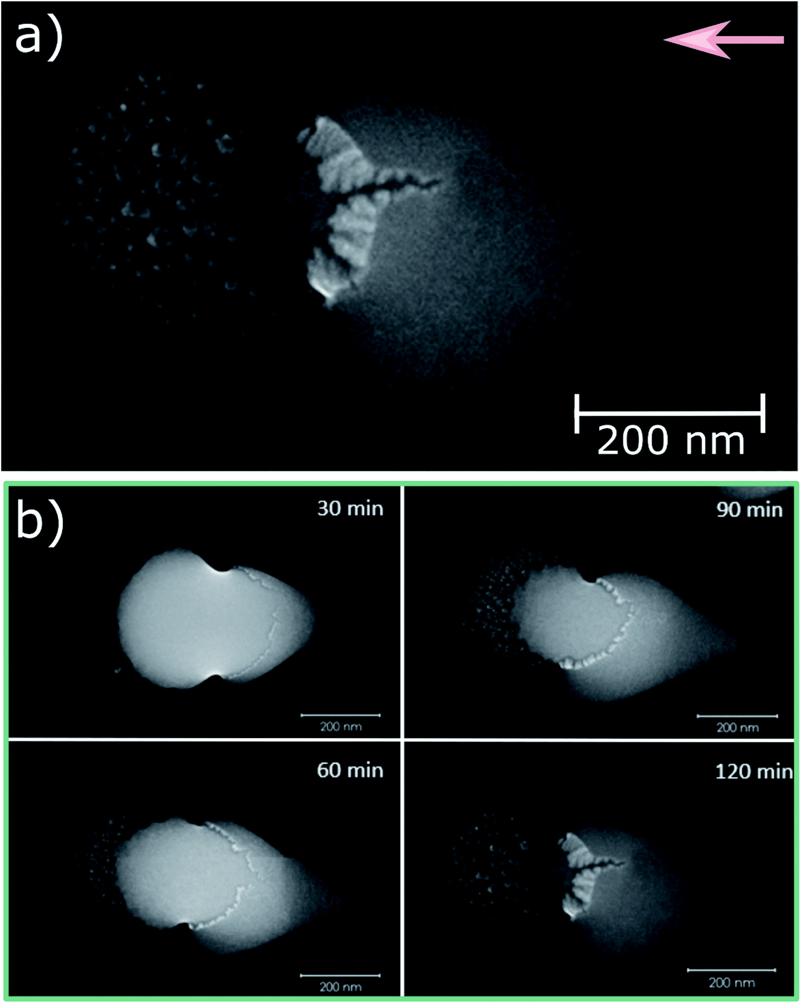 | ||
| Fig. 1 (a) SEM image of a 2D GaN triangle-like nanostructure. (b) Time evolution of this nanostructure upon nitridation. Increasing the time of nitridation leads to the formation of a thin triangle-like structure. Once the original gallium droplet is fully consumed, growth is finished. | ||
We hypothesise that the epitaxial growth of equilateral triangles is governed by a six-fold symmetry of the 2D GaN itself. As is generally known, the triangles are formed from hexagons by a faster growth of one of the faces which in the end leads to its termination. In our case, this is the face directly facing the Ga atomic flux, i.e. being most perpendicular to the nitrogen flux surface projection (indicated by the arrow in Fig. 1a).
In case of a Si substrate with larger miscut angles (i.e. narrower terraces) the triangles were of the opposite orientation (see Fig. S1b†). This is caused by the fact that the fast growing faces reach terrace steps and their motion is stopped. Then the base of the triangle is formed by the growth of slow lateral faces towards these steps.
The growth process of GaN nanostructures was investigated by changing the time of nitridation as illustrated in Fig. 1b. Initially, after the gallium deposition, the silicon surface is covered by liquefied gallium droplets. Once the nitridation is initiated, incoming nitrogen ions start to react with metallic gallium which leads to the formation of a triangle-like GaN structure in the upstream direction with respect to the nitrogen flux surface projection. During this process, the decreasing gallium droplet is asymmetrically dewetted from the silicon surface towards the growing GaN structure. As gallium is gradually consumed in the GaN synthesis process, the triangle-like shaped structure becomes thinner and more prominent. It is obvious that Ga atoms must diffuse across the GaN surface to feed the reaction with nitrogen at the GaN border. It is also clear that the size of the GaN triangles can be controlled by the amount of the source material, i.e. by the size of the initial gallium droplet (see Fig. S1†). The thickness and surface roughness of the analysed triangles were determined by AFM in flat areas of triangles closer to their apexes – i.e. for triangles on substrates with the 0.2° miscut angle roughly at a site at 2/3 of the triangle altitude as marked by the white lines in Fig. S3.† Typical thicknesses of triangles were 13–20 nm and 6–8 nm for the substrates with miscut angles of 0.2° and 4°, respectively (Fig. S4 and S5†).
The corresponding RMS values of surface roughness were 0.7 nm and 0.14 nm for the substrates with miscut angles of 0.2° and 4°, respectively. We have not found an apparent correlation between the island area and their height for the substrate of a given miscut angle.
In the place from where the gallium droplet disappeared, the deteriorated silicon surface was left behind. This phenomenon, referred to as meltback etching and caused by a chemical reaction of gallium with silicon, has been also reported in ref. 23 and by other groups for MOCVD growth of GaN crystals. This etching does not occur in the area of 2D GaN growth because it is most likely outperformed by the Ga reaction with nitrogen species being directly delivered via a hyperthermal nitrogen ion beam to the reaction zone at the GaN border. On the other hand, the left-hand side of the Ga droplet is screened off from the nitrogen flux and thus the Ga etching to the GaN reaction prevails. This explanation is supported by the finding in ref. 23 that addition of N2 to the carrier gas blocks meltback etching.
The effect of post-nitridation was studied by XPS. Fig. 2a shows a Ga 2p3/2 peak measured after 60 min of post-nitridation. The fitting of the Ga 2p3/2 peak revealed the presence of two major components. The first component at 1117.8 eV corresponds to the chemical bonding between Ga atoms in a metallic form (Ga–Ga bonds). The second component at 1119.3 eV represents the chemical bonding between Ga and N in GaN crystals (Ga–N bonds). The fitting parameters of the Ga 2p3/2 peak were reported in ref. 21. The inserted AFM image of a Ga droplet clearly shows that this droplet is not fully transformed into 2D GaN. Fig. 2b shows the Ga 2p3/2 peak after 120 min of post-nitridation. Both peak components – Ga–Ga and Ga–N – are still present in the spectra. However, the Ga–N component is much more prominent than the Ga–Ga one which suggests that most of the metallic gallium from Ga droplets has been transformed into the GaN compound, which is also supported by the inserted AFM image of an analyzed structure. The fragment of Ga–Ga bonding most likely comes from the unconsumed original Ga droplet and possibly also from the deteriorated silicon surface.
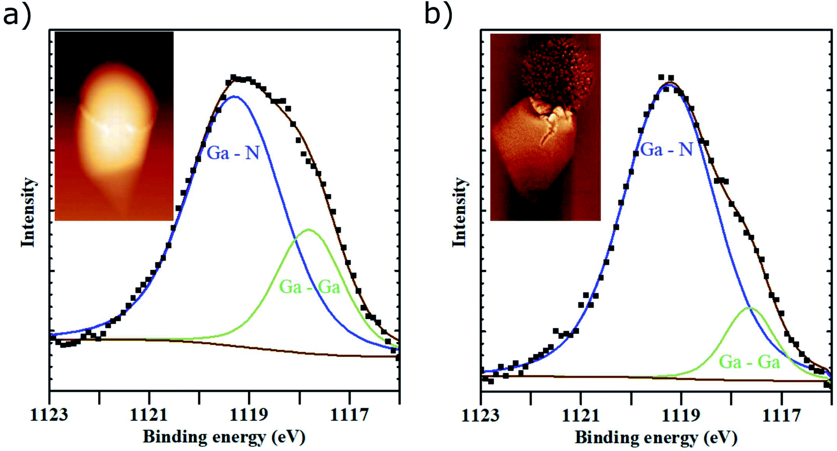 | ||
| Fig. 2 Fitted XPS Ga 2p3/2 peak obtained during the post-nitridation after (a) 60 min and (b) 120 min. The Ga–Ga component is at 1117.8 eV (green curve) and the Ga–N component at 1119.3 eV (blue curve). | ||
Interestingly, some unidentified minor peaks located at approximately 1121.0 eV and 1118.2 eV and related to an intermediate product after 60 minutes of post-nitridation are not present in the overall XPS peak in Fig. 2b corresponding to the more progressed nitridation.
To elucidate the elemental component distribution in the individual nanostructures, Auger nanoanalysis by NanoSAM was performed. There are three different selected regions A, B and C in the SEM image of the nanostructure in Fig. 3a. Region A corresponds to the original Si(111) surface far away from the droplet and nanostructure, region B corresponds to the triangle-like nanostructure, and region C represents the peripheral area of the original gallium droplet. Fig. 3b shows the signal of Auger electrons in the range of kinetic energy corresponding to Ga atoms. Gallium is present in the triangle-like shaped nanostructure (B), as well as in the interface area between the original Ga droplet and the GaN triangle (C). Gallium atoms are not present in region A. Fig. 3c shows the signal of Auger electrons in the energy range corresponding to N atoms. The presence of nitrogen in region A indicates that nitrogen ions react with the pristine silicon surface and form a thin layer of silicon nitride. Nitrogen is also present in the triangle-like GaN structure (region B). However, there is no evidence of nitrogen in the area of the original gallium droplet (region C). Such results lead us to the conclusion that nitrogen ions do not penetrate into the Ga droplet and thus do not form Ga–N bonds here. As proposed by Gerlach et al.,20 nitrogen ions rather diffuse along the liquid–vapor interface (Ga droplet surface) to peripheral regions of the droplet–substrate interface (triple point, i.e. the solid–liquid–vapor interface). At this interface, the nucleation of GaN is initiated which eventually results in the formation of a 2D GaN layer.
 | ||
| Fig. 3 Elemental analysis of a triangle-like GaN nanostructure carried out by NanoSAM. (a) SEM image of the studied structure with the selected regions A, B and C. (b) Gallium and (c) nitrogen abundance in the selected regions. | ||
A STEM image of a cross-sectional lamella (Fig. 4a) reveals sharp interfaces between the Si(111) substrate and the amorphous gallium droplet, and between this substrate and the crystalline hexagonal GaN. Fig. 4b shows a zoom-in of the 2D GaN–Si(111) interface. It reveals the presence of crystallographic defects spreading over 3–4 MLs. As the thickness of the nanocrystals is substantially higher, these defects should not influence the properties of 2D nanocrystals themselves. The observed interlayer distance of 3.15 ± 0.09 Å in the 2D GaN structure is significantly larger than the values of 2.59 Å (ref. 18 and 24) and 2.70 Å (ref. 14) found experimentally in wurtzite GaN crystals. The calculated interlayer distance for layered 2D GaN varied from 2.22 Å (ref. 25) to 3.10 Å,26,27 depending on the type of numerical simulation used. Unlike van der Waals structures such as graphite and others, 2D GaN transforms into different crystalline structures due to the formation of vertical bonds between the Ga and N atoms of neighboring layers. Thus, more than three different stable types of 2D GaN stacking were predicted,26 and, hence, a variety of different interlayer distances can be observed. The measured lattice parameter a was 3.29 ± 0.13 Å which is in principle also convincingly higher than in the wurtzite GaN (3.18 Å).24,28,29 On top of that, it is very close to the calculated and experimental values for 2D GaN (e.g. 3.28 Å in ref. 30 and 3.32 Å in ref. 14, resp.).
 | ||
| Fig. 4 (a) STEM image of the cross-sectional lamella of an amorphous gallium droplet and crystalline GaN on the Si(111) 7 × 7 substrate. (b) Zoomed-in STEM image of the 2D GaN–Si(111) 7 × 7 interface. | ||
To summarize, the experimental results of our STEM analysis are both in qualitative and quantitative agreement with the literature on lattice parameters of 2D GaN nanocrystals, and different from those known for wurtzite GaN.
Fig. 5 shows the EDX measurement of gallium and nitrogen elemental abundance in the 2D GaN structure. While gallium is detected in the whole structure, i.e. in the original gallium droplet and in the formed 2D GaN layered nanostructure, nitrogen is present exclusively in the region of 2D GaN. Such a result corresponds to the Auger microanalysis results discussed above and supports the conclusion that nitrogen atoms are not present in the gallium droplet.
 | ||
| Fig. 5 EDX maps of the cross-sectional lamella of an amorphous gallium droplet and crystalline GaN on the Si(111) 7 × 7 substrate. While gallium is present in the crystalline structure (area encircled by the yellow loop) as well as in the amorphous droplet (blue loop), nitrogen is present exclusively in the crystalline 2D GaN nanostructure. | ||
4. Conclusion
A low temperature droplet epitaxy with the assistance of hyperthermal nitrogen ions was successfully utilized for fabrication of planar GaN triangular nanocrystals with a crystal structure different from that of wurtzite GaN and qualitatively and quantitatively corresponding to that of 2D GaN nanocrystals. The STEM imaging of a cross-sectional lamella revealed an interlayer spacing distance of 3.15 ± 0.09 Å which is higher than in the case of wurtzite GaN by at least 17%, but in agreement with the presented values calculated for 2D GaN structures. The lattice parameter of 3.29 ± 0.13 Å found by the same method is convincingly higher than in the wurtzite GaN (3.18 Å) and in very good agreement with the calculated values. The Auger nanoanalysis and EDX measurement indicated that nitrogen particles do not penetrate into the Ga droplets, but diffuse along their surface towards the liquid–solid interface at the periphery of the droplet. Here, the nuclei of GaN are created which consequently leads to the formation of the triangle-like 2D GaN nanostructures. The nanostructures grow at their borders via a reaction between Ga atoms delivered here from the original droplets and incoming nitrogen species. In the place from where the gallium droplet disappeared, the deteriorated silicon surface was left behind. The 2D GaN nanostructures are ready for the exploration of their optical and electrical properties. This will become the topic of our next experiments.Conflicts of interest
There are no conflicts to declare.Acknowledgements
We acknowledge the support by the Czech Science Foundation (grant no. 20-28573S), European Commission (H2020-Twininning project no. 810626 – SINNCE, M-ERA NET HYSUCAP/TACR-TH71020004), BUT – specific research no. FSI-S-20-6485, and Ministry of Education, Youth and Sports of the Czech Republic (CzechNanoLab Research Infrastructure – LM2018110).References
- N. Sanders, D. Bayerl, G. Shi, K. A. Mengle and E. Kioupakis, Electronic and Optical Properties of Two-Dimensional GaN from First-Principles, Nano Lett., 2017, 17(12), 7345–7349 CrossRef CAS PubMed.
- C. Feng, H. Qin, D. Yang and G. Zhang, First-principles investigation of the adsorption behaviors of CH2O on BN, AlN, GaN, InN, BP, and P monolayers, Materials, 2019, 12(4), 676 CrossRef CAS PubMed.
- C. Pashartis and O. Rubel, Alloying strategy for two-dimensional GaN optical emitters, Phys. Rev. B, 2017, 96(15), 1–6 CrossRef.
- S. Pimputkar, J. S. Speck, S. P. Denbaars and S. Nakamura, Prospects for LED lighting, Nat. Photonics, 2009, 3(4), 180–182 CrossRef CAS.
- M. Chhowalla, D. Jena and H. Zhang, Two-dimensional semiconductors for transistors, Nat. Rev. Mater., 2016, 1(16052), 1–15 Search PubMed.
- Q. Hao, H. Zhao and Y. Xiao, A hybrid simulation technique for electrothermal studies of two-dimensional GaN-on-SiC high electron mobility transistors, J. Appl. Phys., 2017, 121(20), 204501 CrossRef.
- X. Zhang, L. Jin, X. Dai, G. Chen and G. Liu, Two-Dimensional GaN: An Excellent Electrode Material Providing Fast Ion Diffusion and High Storage Capacity for Li-Ion and Na-Ion Batteries, ACS Appl. Mater. Interfaces, 2018, 10(45), 38978–38984 CrossRef CAS PubMed.
- F. Hussain, et al., Enhanced ferromagnetic properties of Cu doped two-dimensional GaN monolayer, Int. J. Mod. Phys. C, 2015, 26(1), 1–8 CrossRef.
- N. Alaal and I. S. Roqan, Tuning the Electronic Properties of Hexagonal Two-Dimensional GaN Monolayers via Doping for Enhanced Optoelectronic Applications, ACS Appl. Nano Mater., 2019, 2(1), 202–213 CrossRef CAS.
- R. González, W. López-Pérez, Á. González-García, M. G. Moreno-Armenta and R. González-Hernández, Vacancy charged defects in two-dimensional GaN, Appl. Surf. Sci., 2018, 433, 1049–1055 CrossRef.
- L. Tong, et al., Anisotropic carrier mobility in buckled two-dimensional GaN, Phys. Chem. Chem. Phys., 2017, 19(34), 23492–23496 RSC.
- Z. Y. Al Balushi, et al., Two-dimensional gallium nitride realized via graphene encapsulation, Nat. Mater., 2016, 15(11), 1166–1171 CrossRef CAS PubMed.
- W. Wang, Y. Li, Y. Zheng, X. Li, L. Huang and G. Li, Lattice Structure and Bandgap Control of 2D GaN Grown on Graphene/Si Heterostructures, Small, 2019, 15(14), 1–8 Search PubMed.
- Y. Chen, et al., Growth of 2D GaN Single Crystals on Liquid Metals, J. Am. Chem. Soc., 2018, 140(48), 16392–16395 CrossRef CAS PubMed.
- N. Koguchi and K. Ishige, Growth of GaAs epitaxial microcrystals on an S-terminated GaAs substrate by successive irradiation of Ga and as molecular beams, Jpn. J. Appl. Phys., Part 1, 1993, 32(5), 2052–2058 CrossRef CAS.
- J. Stangl, V. Holý and G. Bauer, Structural properties of self-organized semiconductor nanostructures, Rev. Mod. Phys., 2004, 76(3), 725–783 CrossRef CAS.
- S. Bietti, C. Somaschini and S. Sanguinetti, Crystallization kinetics of Ga metallic nano-droplets under As flux, Nanotechnology, 2013, 24(20), 205603 CrossRef CAS PubMed.
- J. Mach, et al., An ultra-low energy (30-200eV) ion-atomic beam source for ion-beam-assisted deposition in ultrahigh vacuum, Rev. Sci. Instrum., 2011, 82(8), 083302 CrossRef PubMed.
- J. Mach, et al., Optimization of ion-atomic beam source for deposition of GaN ultrathin films, Rev. Sci. Instrum., 2014, 85(8), 083302 CrossRef PubMed.
- J. W. Gerlach, T. Ivanov, L. Neumann, T. Höche, D. Hirsch and B. Rauschenbach, Epitaxial GaN films by hyperthermal ion-beam nitridation of Ga droplets, J. Appl. Phys., 2012, 111(11), 113521 CrossRef.
- J. Mach, et al., Low temperature selective growth of GaN single crystals on pre-patterned Si substrates, Appl. Surf. Sci., 2019, 497, 143705 CrossRef CAS.
- M. Kolíbal, T. Čechal, E. Brandejsová, J. Čechal and T. Šikola, Self-limiting cyclic growth of gallium droplets on Si(111), Nanotechnology, 2008, 19(47), 475606 CrossRef PubMed.
- M. Khoury, O. Tottereau, G. Feuillet, P. Vennéguès and J. Zúñiga-Pérez, Evolution and prevention of meltback etching: case study of semipolar GaN growth on patterned silicon substrates, J. Appl. Phys., 2017, 122(10), 1–7 CrossRef.
- C. G. Van de Walle, Effects of impurities on the lattice parameters of GaN, Phys. Rev. B: Condens. Matter Mater. Phys., 2003, 68(16), 1–5 CrossRef.
- Y. Gao and S. Okada, Energetics and electronic structures of thin films and heterostructures of a hexagonal GaN sheet, Jpn. J. Appl. Phys., 2017, 56(6), 065201 CrossRef.
- A. Onen, D. Kecik, E. Durgun and S. Ciraci, GaN: from three- to two-dimensional single-layer crystal and its multilayer van der Waals solids, Phys. Rev. B, 2016, 93(8), 1–11 CrossRef.
- A. Onen, D. Kecik, E. Durgun and S. Ciraci, Onset of vertical bonds in new GaN multilayers: beyond van der Waals solids, Nanoscale, 2018, 10(46), 21842–21850 RSC.
- M. Leszczynski, et al., Lattice parameters of gallium nitride, Appl. Phys. Lett., 1996, 69(1), 73–75 CrossRef CAS.
- V. Darakchieva, P. P. Paskov, T. Paskova, E. Valcheva, B. Monemar and M. Heuken, Lattice parameters of GaN layers grown on a-plane sapphire: effect of in-plane strain anisotropy, Appl. Phys. Lett., 2003, 82(5), 703–705 CrossRef CAS.
- C. Yelgel, First-principles modeling of GaN/MoSe2 van der Waals heterobilayer, Turk. J. Phys., 2017, 41(5), 463–468 CrossRef CAS.
Footnote |
| † Electronic supplementary information (ESI) available. See https://doi.org/10.1039/d2na00175f |
| This journal is © The Royal Society of Chemistry 2022 |