
 Open Access Article
 This Open Access Article is licensed under a Creative Commons Attribution-Non Commercial 3.0 Unported Licence
Formation and growth characteristics of nanostructured carbon films on nascent Ag clusters during room-temperature electrochemical CO2 reduction†
Suthasinee
Watmanee
a,
Rungkiat
Nganglumpoon
a,
Nattaphon
Hongrutai
a,
Piriya
Pinthong
a,
Piyasan
Praserthdam
 a,
Suttipong
Wannapaiboon
b,
Petra Ágota
Szilágyi
c,
Yoshitada
Morikawa
d and
Joongjai
Panpranot
*aefg
a,
Suttipong
Wannapaiboon
b,
Petra Ágota
Szilágyi
c,
Yoshitada
Morikawa
d and
Joongjai
Panpranot
*aefg
aCenter of Excellence on Catalysis and Catalytic Reaction Engineering, Biorefinery Cluster, Department of Chemical Engineering, Faculty of Engineering, Chulalongkorn University, Bangkok 10330, Thailand. E-mail: joongjai.p@chula.ac.th
bSynchrotron Light Research Institute (Public Organization), 111 University Avenue, Suranaree, Muang, Nakhon Ratchasima, 30000, Thailand
cSchool of Engineering and Materials Science, Queen Mary University of London, Mile End Road, E1 4NS London, UK
dDepartment of Precision Engineering, Graduate School of Engineering, Osaka University, Osaka, Japan
eGraphene Electronics Research Unit, Faculty of Science, Chulalongkorn University, Bangkok, 10330, Thailand
fDepartment of Chemical & Petroleum Engineering, Faculty of Engineering, Technology and Built Environment, UCSI University, 56000, Kuala Lumpur, Malaysia
gBio-Circular-Green-economy Technology & Engineering Center, BCGeTEC, Faculty of Engineering, Chulalongkorn University, Bangkok, Thailand 10330
First published on 11th March 2022
Abstract
Synthesis of carbon nanostructures at room temperature and under atmospheric pressure is challenging but it can provide significant impact on the development of many future advanced technologies. Here, the formation and growth characteristics of nanostructured carbon films on nascent Ag clusters during room-temperature electrochemical CO2 reduction reactions (CO2RR) are demonstrated. Under a ternary electrolyte system containing [BMIm]+[BF4]−, propylene carbonate, and water, a mixture of sp2/sp3 carbon allotropes were grown on the facets of Ag nanocrystals as building blocks. We show that (i) upon sufficient energy supplied by an electric field, (ii) the presence of negatively charged nascent Ag clusters, and (iii) as a function of how far the C–C coupling reaction of CO2RR (10–390 min) has advanced, the growth of nanostructured carbon can be divided into three stages: Stage 1: sp3-rich carbon and diamond seed formation; stage 2: diamond growth and diamond–graphite transformation; and stage 3: amorphous carbon formation. The conversion of CO2 and high selectivity for the solid carbon products (>95%) were maintained during the full CO2RR reaction length of 390 min. The results enable further design of the room-temperature production of nanostructured carbon allotropes and/or the corresponding metal-composites by a viable negative CO2 emission technology.
1. Introduction
Synthetic carbon allotropes (SCAs) represent one of the most promising emerging materials families with enormous potential for high-performance applications. They have been exploited in the development of advanced technology for biomedical, electronics, renewable energy, sensors, membranes, and materials synthesis.1,2 The commercial main-stream production of SCAs, however, has relied on either pyrolysis, chemical vapor deposition, arc discharge, laser ablation, or exfoliation, each of which display major shortcomings due to being energy-intensive.3–8In a recent study by Dai et al.,9 various carbon nanostructures were synthesized under ambient conditions with ethanol as the carbon source, using KOH and ultrasonic shock. The carbon nanostructures were grown directly from the carbon atoms and small carbon groups, which were formed in the solution. After 5 days, sp2-carbon seed grew and developed into defective nanotubes, single-core carbon-onions, and graphene polyhedra, which further transformed to multicore carbon-onion and graphene after 8 and 14 days, respectively. Without ultrasonic shock, the formation of sp3-structure n-diamond was observed after 14 days. However, most of these carbons turned amorphous after 30 days with or without ultrasonic shock. The process yielded small amounts of the carbon products and long reaction times were required most likely owing to the low activation energy of the process.
An alternative, interesting and viable solid-carbon production approach is the room temperature CO2RR that can convert the greenhouse gas CO2 into value-added nanostructured carbon materials, thus reducing the climate-change effects through a negative CO2 emission technology. Esrafilzadeh et al.10 showed that amorphous carbonaceous species and some graphitic products can be produced by room temperature CO2RR using galinstan liquid metal electrocatalysts containing cerium metal nanoparticles. The incorporated Ce from the reduction of Ce3+ to Ce0 forms nanoparticles on the liquid metal electrode. The pyrophoric nature of Ce was suggested to result in its high activity in the catalytic process for CO2RR. However, the solid carbon products were mostly amorphous carbon. More recently, we have reported the formation of nanostructured carbon allotropes including 3D-nano graphene and single crystalline nanodiamond at room temperature, on various metal electrocatalysts such as Bi, Ag, Co, and Zn under the dynamic CO2RR environment.11 The nanostructured carbon allotropes were grown on the metal nanocrystal facets formed upon reduction and nanoclustering of the natural ultra-thin oxide layers of the electrocatalyst in the ternary electrolyte system containing [BMIM]+[BF4]−/propylene carbonate/H2O at relatively low applied potentials between −1.1 to −1.6 V vs. Ag/AgCl. However, the growth mechanism for the formation of carbon allotropes under the above-mentioned CO2RR system has not yet been discovered. The formation and growth characteristics of nanocrystalline carbon films are crucial for controlling their quality and structure in the process.
The present work uncovers and reports in-depth understanding of the evolution of nanostructured carbon films grown on Ag nanocrystals during CO2RR under ambient conditions. The synthesized nanostructured Ag–C films obtained at 10, 20, 30, 70, 140, and 390 min reaction time were characterized by various techniques including Raman spectroscopy, TEM-SAED-EDX, and GI-XRD. The Ag electrocatalysts' performance in CO2RR was also evaluated for CO2 conversion, product selectivity, and stability under reaction conditions.
2. Experimental
2.1 Ag-electrocatalyst preparation
The copper substrate (thickness 0.1 mm, Alfa Aesar, 99.9999%) was mechanically polished using 800 grit sandpaper until a shiny and visually smooth surface was obtained. The Ag-electrocatalysts were prepared by electrochemical deposition process, which was conducted using a two-electrode system consisting of a copper substrate cathode and a platinum rod anode. The electrolyte solution contained AgNO3 (0.01 M) in (NH4)2SO4 (0.6 M). The deposition of the Ag metal electrocatalyst on the substrate in a square shape with a working area of 1 × 1 cm2 was conducted as follows; firstly, the substrate was immersed in the electrolyte solution and a constant electrical potential of −1.1 V was applied for 200 s; after the electrodeposition process was completed, the sample was removed and washed with deionized water; finally, the sample was dried overnight under ambient conditions, before being used as electrocatalyst (denoted as Ag-electrocatalyst). All chemicals were purchased from Sigma-Aldrich and were used without further purification.2.2 CO2RR measurements
The CO2RR measurements were performed in an H-cell type reactor consisting of a three-electrode system including working, reference, and counter electrodes with a potentiostat (Multi Autolab (M204), Metrohm). A Pt plate (50 mm × 50 mm) was used as a counter electrode and the anodic chamber contained 20 cm3 of KHCO3 (0.1 M). A Ag/AgCl reference was served as the reference electrode and the as-prepared Ag-electrocatalyst was employed as the working electrode. In the cathodic chamber, containing 20 cm3 of the mixture of [BMIM]+[BF4]−/propylene carbonate/H2O with the volume ratio of approximately 4![[thin space (1/6-em)]](https://www.rsc.org/images/entities/char_2009.gif) :5:1, CO2 (100 cm3 min−1, 99.99% Linde) was purged with a high flow rate (100 cm3 min−1), into the electrolyte for 60 min to ensure the liquid electrolyte was fully saturated with CO2 before CO2RR. During the experiments, CO2 was continuously purged at a slow rate (20 cm3 min−1) into the electrolyte and an electrical current was simultaneously applied at −1.6 V. for 10, 20, 30, 70, 140, and 390 min (denoted as Ag-x, where x is the reaction time). After the electrochemical reaction, the working electrodes were collected and washed with DI-water before further analysis. The electrochemically produced gases were analyzed using gas chromatography (GC-2014, Shimadzu) equipped with a thermal conductivity detector. Liquid products were analyzed using 13C-NMR and 1H-NMR. The percent CO2 conversion was calculated according to eqn (1).
:5:1, CO2 (100 cm3 min−1, 99.99% Linde) was purged with a high flow rate (100 cm3 min−1), into the electrolyte for 60 min to ensure the liquid electrolyte was fully saturated with CO2 before CO2RR. During the experiments, CO2 was continuously purged at a slow rate (20 cm3 min−1) into the electrolyte and an electrical current was simultaneously applied at −1.6 V. for 10, 20, 30, 70, 140, and 390 min (denoted as Ag-x, where x is the reaction time). After the electrochemical reaction, the working electrodes were collected and washed with DI-water before further analysis. The electrochemically produced gases were analyzed using gas chromatography (GC-2014, Shimadzu) equipped with a thermal conductivity detector. Liquid products were analyzed using 13C-NMR and 1H-NMR. The percent CO2 conversion was calculated according to eqn (1). | (1) |
The selectivity of solid carbon products was calculated based on the amount of CO2 being converted (mole CO2 conversion from GC results). Besides the solid carbon products, small amounts of gaseous CO were detected as the only by-product with trace amount of liquid products. The percent selectivity of solid carbon products was calculated by eqn (2).
 | (2) |
2.3 Characterization techniques
Raman spectra were acquired on a PerkinElmer Spectrum GX using the UV line at 532 nm and a TE-cooled CCD detector. The laser output was 10 mW. Scanning electron microscope with energy dispersive X-ray analysis (SEM-EDX, JEOL JSM-5800LV) was used to characterize the morphologies of the solid products. Transmission electron microscopy (TEM) with EDX and selected area electron diffraction (SAED) was performed on a JEOL (JEM-2010). The TEM-EDX-SAED samples were prepared by dispersing the catalyst in ethanol with a few drops of the resulting suspension deposited on the TEM grid. After that, the samples were observed with a TECNAI G2 Spirit Twin from FEI. Focused ion beam field emission scanning electron microscopy (FIB-SEM) was performed on a FEI with model Versa 3D. To analyze element states of the electrocatalysts, X-ray photoelectron spectra (XPS) were collected on an Amicus spectrometer using Mg Kα X-ray radiation operated at a voltage of 10 kV and a current of 20 mA. Solution-state NMR spectra of the electrolyte were measured on Bruker AV400 ultra shield using the topspin 2.1 software. The crystallographic orientation of thin films was probed by grazing incidence X-ray diffraction (GIXRD) at an incident angle of 3° at 12 keV (wavelength of 0.103 nm) with respect to the substrate surface. The results were calculated based on Cu-Kα (wavelength of 0.154 nm). The measurement was performed at the BL1.1W beamline of the Synchrotron Light Research and Institute (Public Organization) at the Synchrotron Thailand Central Lab. In situ X-ray absorption spectroscopy (XAS) and X-ray absorption near-edge spectroscopy (XANES) were performed on the silver L3-edge in fluorescence mode at the BL8 beamline of the Synchrotron Light Research and Institute (Public Organization) at the Synchrotron Thailand Central Lab, using the IO ionization chamber and 19-element Ge detectors for measuring fluorescence beam intensities before and after passing the samples, respectively. In addition, Ag foil was used as a reference to detect the beam, for energy calibration, and alignment purposes. Data processing and analysis were performed using the Athena software. The in situ XAS spectra were collected at room temperature under He atmosphere. The liquid state 13C-NMR and 1H-NMR were measured by Fourier transform nuclear magnetic resonance spectrometer (Bruker AV400 ultra shield) 400 MHz and d6-DMSO was used as solvent.3. Results and discussion
The CO2RR to nanocrystalline carbon products was carried out on the Ag-electrocatalysts, which were prepared by the facile electrochemical deposition method, in the ternary electrolyte system containing [BMIM]+[BF4]−/propylene carbonate/H2O at ambient conditions with −1.6 V vs. Ag/AgCl applied potential for different reaction times (10, 20, 30, 70, 140, and 390 min). Briefly, upon applying the negative potential, nanoclustering of the self-limiting ultrathin oxides layers of Ag particles occurred on the highly conductive Cu substrate leading to the formation of negatively charged metallic Ag clusters, stabilized by the ternary electrolyte system.11 This electrochemically driven nano-catalytic system allows for the reduction of CO2 into single atom C* and the subsequent growth of carbon allotropes on the nascent metal nanocrystals' facet building blocks. In this study, the metal–carbon (Ag–C) composites obtained from CO2RR for each reaction length, were extensively characterized in order to elucidate the evolution of the nanostructured carbon films on the Ag single crystal formed under the CO2RR environment. The growth of carbon allotropes under the room temperature CO2RR can be rationalised in three consecutive stages:(1) The first stage is sp3-rich and diamond seed formation, which occurs instantaneously with the Ag nanoclustering;
(2) Then the electrocrystallization of carbon atoms continues to grow on the preferable orientations of the Ag single crystals leading to the formation of single crystalline nanodiamond films; and
(3) As the reaction time is prolonged, the reaction eventually results in amorphous carbon covering the single crystalline nanodiamond films.
3.1 The evolution of nanostructure Ag–C formation during the initial stage CO2RR (stage 1: sp3-rich carbon and diamond seed formation)
The morphology of the electrocatalysts observed from SEM micrographs before and after CO2RR for 10 and 20 min are shown in Fig. 1. At the initial stage of CO2RR, for 10 and 20 min time on stream, evolution of Ag particles deposited on the Cu foil substrate started to occur. The prepared Ag electrocatalyst before CO2RR showed multi-pods or flower-like nanoplates morphologies (see Fig. 1-A1). After 10 min CO2RR, the flower-like nanoplates were transformed into small-branched Ag dendrites nanostructures especially at the tips of the flower-like nanoplates12 (Fig. 1-B1). As the CO2RR reaction time increased to 20 min, the small-branched Ag dendrites became larger and longer (Fig. 1-C1). Due to low concentration of Ag precursor under the electrodeposition conditions used, Ag dendritic structure is expected.13 Such results provide evidence for nanoclustering of the particulate Ag electrocatalysts on the Cu foil substrate. Upon applying a negative potential, Ag atoms could be partly locally exsolved out of the oxide lattice and intrinsically combined with each other, forming single crystalline nanoparticles that grew by direct attachment until they reach a metastable size.14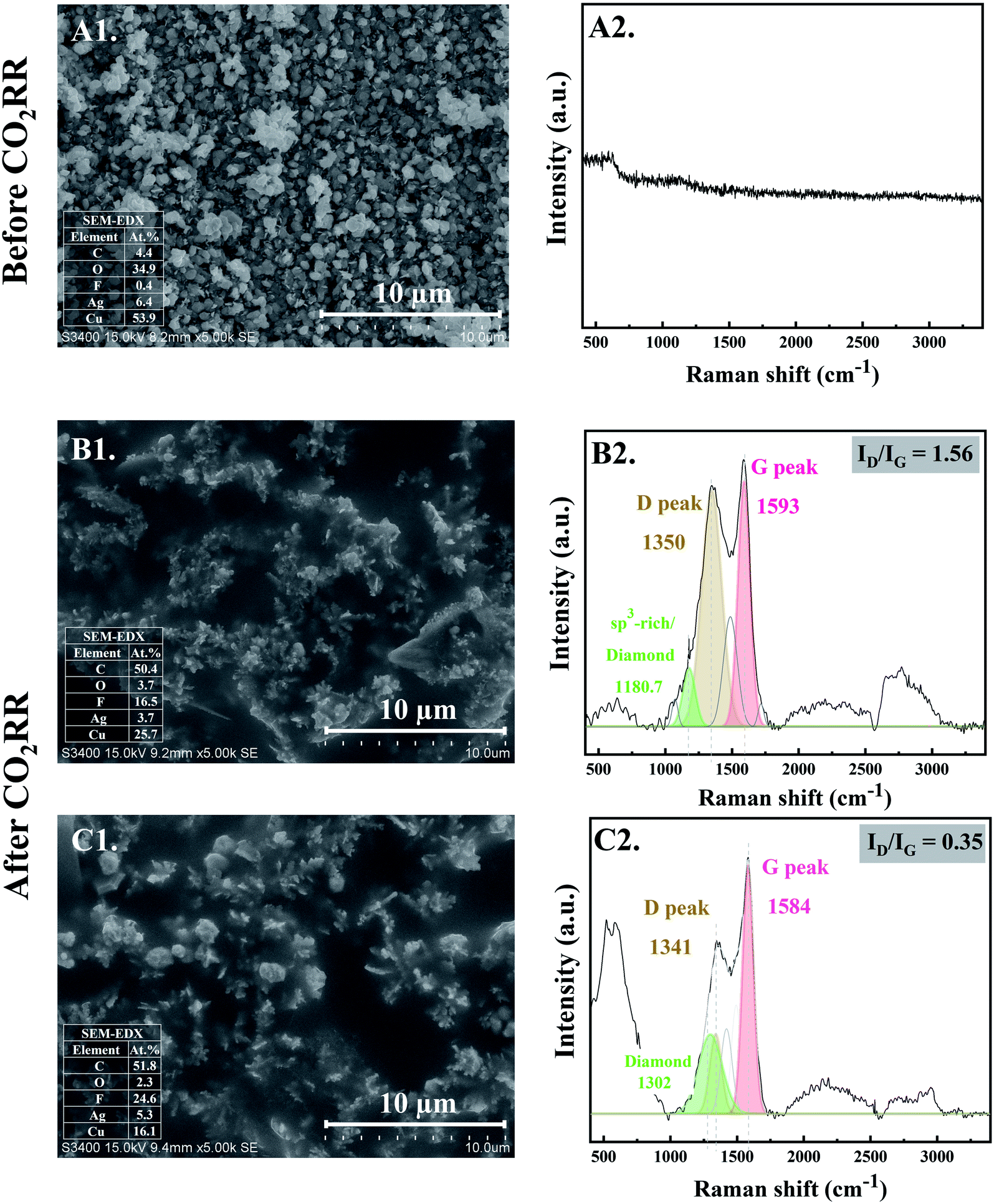 | ||
| Fig. 1 SEM images with EDX (Left column) and Raman spectra (Right column) of the Ag-electrocatalyst before CO2RR (A1 and A2) and after CO2RR at ambient conditions for 10 min (B1 and B2) and 20 min (C1 and C2). | ||
At the same time, the evolution of nanostructured carbon produced from CO2RR also takes place. Their characteristics were investigated by Raman spectroscopy. Fig. 1-B2 and C2 reveal the time dependent ex situ Raman spectra of the carbon products obtained after CO2RR for 10 and 20 min on stream, respectively. The Raman spectra corresponding to carbon species were clearly detected at the initial stage of CO2RR for 10 min. The Raman spectra of both Ag-10 and Ag-20 samples composed of disordered carbon structures as illustrated by the D and G peaks at around 1350 cm−1 (FWHM of 176 cm−1) and 1593 cm−1 (FWHM of 109 cm−1), respectively. The D and G bands are ascribed to defects induced on the sp3 hybridized hexagonal sheet of carbon (D band: disorders and defects in sp3 carbon) and graphitic signature of carbon sp2 hybridization (G band: graphite structure), respectively.15 Moreover, the deconvolution of Raman spectra of Ag-10 and Ag-20 showed a downshift of the center peaks of D and G band from 1350 to 1341 (FWHM of 107 cm−1) and from 1593 to 1584 (FWHM of 98 cm−1), respectively. Such shifting of peaks is specific to changes of the chemical bonds and/or the symmetry of molecules with reaction time; it suggests that rearrangement of atomic C (electro-crystallization) occurred on the Ag crystal as the reaction time was prolonged. A significant downshift of these bands also implies the presence of lower degree of amorphous carbon.16 In addition, the ratio of the intensity of the D band and G band (ID/IG) decreased with increasing reaction time from 10 min to 20 min, indicating that the crystallization of carbon allotropes was improved with time spent on stream. Additionally, the Raman peak at ∼1180 cm−1, apparent for the Ag-10 sample can be attributed to the presence of an sp3-rich phase. For Ag-20, a Raman band centered at ∼1302 cm−1 was observed, which can be related to diamond species;17 it suggests an early stage of the nanocrystalline diamond formation (i.e. formation of diamond seed). The Raman results are consistent with the increase in carbon content from 4.4 at% of the Ag-electrocatalyst before CO2RR to 50.4 at% and 51.8 at% after 10 min and 20 min CO2RR, respectively, as shown by SEM-EDX.
3.2 The evolution of nanostructure Ag–C formation during the middle stage CO2RR (stage 2: diamond growth and diamond–graphite transformation)
When CO2RR reaction time increased to 30 min, bigger, longer, and more complex Ag dendrites were formed as shown in Fig. 2-D1. While for 70 min reaction time, a long main trunk with secondary or hierarchically branches of the Ag dendrites were obtained (Fig. 2-E1). When the time on stream was further increased to 140 min, the dendrites greatly extended both laterally and vertically to form a small “fern-leaf” structure (Fig. 2-F1). This is consistent with the Ag micro/nanostructure generally formed under similar electrodeposition conditions, as the deposition time increases.12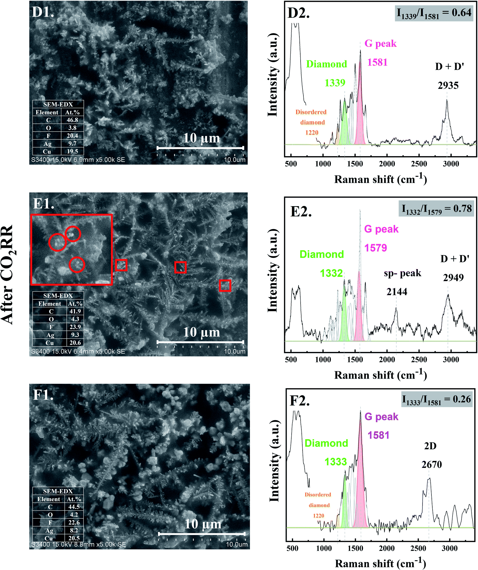 | ||
| Fig. 2 SEM images with EDX (Left column) and Raman spectra (Right column) of the Ag-electrocatalyst after CO2RR at ambient conditions for 30 min (D1 and D2), 70 min (E1 and E2), and 140 min (F1 and F2). | ||
As concluded from the SEM and Raman results, arrangement of single atoms C* into nanostructured carbon allotropes takes place simultaneously during the dynamic changes of the Ag-electrocatalysts under the CO2RR conditions. The evolution of the nanostructured carbon allotropes is distinctively observed after CO2RR for 30 min. Additional peaks corresponding to different types of sp2 and sp3 defects, as often found in defective nanocrystalline diamond films, are apparent (Fig. 2-D2). The Raman shift at ∼1339 cm−1 represents crystalline diamond with several disordered diamond structures (represented by Raman band at 1220 cm−1).18 The peaks at ∼1500 cm−1 and ∼1580 cm−1 were attributed to the disordered sp3-carbon and monocrystalline graphite, respectively.18,19 The sharp peak at ∼1660 cm−1 was assigned to a particularly stable defect in diamond, a so-called “dumbbell” split-interstitial defect consisting of an isolated sp2 bonded pair.20 There are a number of peaks in the 1100–1250 cm−1 region of the Raman spectra, representing modes of trans-polyacetylene segments formed on the intercrystalline boundaries of diamond grains.21 Moreover, the Raman band at 2935 cm−1, attributed to C–H stretch in graphite or the presence of poorly ordered carbon,22 was also detected for Ag-30.
After 70 min time on stream (see Fig. 2-E2), the Ag-70 shows essentially similar Raman spectra as that of Ag-30. However, the Raman peak of diamond shifted from 1339 cm−1 to 1332 cm−1 with higher value of Idiamond/IG (I1332/I1579 of Ag-70 = 0.78) compared with that of Ag-30 (I1339/I1581 = 0.64). The full-width at half peak maximum (FWHM) of the diamond peaks of Ag-30, and Ag-70 was around 79 and 63 cm−1, respectively. This suggests that the nanodiamond being formed was in the nanometer size regime, or it contained abundant planar defects.23 In addition, the Ag-70 exhibited a Raman band at ∼2144 cm−1, which is assigned to C![[triple bond, length as m-dash]](https://www.rsc.org/images/entities/char_e002.gif) C bonds in a linear carbon chain, consisting of alternating single and triple bonds with sp hybridization. This Raman band has been reported to represent a key intermediate metastable phase in the diamond-to-graphite transformation.22
C bonds in a linear carbon chain, consisting of alternating single and triple bonds with sp hybridization. This Raman band has been reported to represent a key intermediate metastable phase in the diamond-to-graphite transformation.22
Interestingly, although there was no significant change of the Raman spectra for the carbon products obtained after CO2RR of Ag-140, compared with Ag-30 and Ag-70, the Idiamond/IG (I1333/I1581) drastically decreased to 0.26 (Fig. 2-F2). Moreover, an additional peak at 2670 cm−1, which represents G′ (or 2D) band,24,25 was remarkably observed whereas the peak at around 2100 cm−1 disappeared. The shape of G′, or 2D, region in the range of 2400 to 3250 cm−1 is typically affected from the defect structures of graphite.24 These Raman bands also suggest that carbon nanotubes (CNTs) may have formed. It was previously reported that nanosized diamond particles can act as nuclei for CNTs growth during the CVD process.26
As shown in the SEM micrographs, small bright granules are noticeable on the tips of Ag-dendrites after CO2RR for 70 min (marked in the red rectangle in Fig. 2-E1). This is likely due to the nucleation and growth of nanodiamond structures on the tips of the Ag-dendrites, where electric field is the highest.27 In other words, the reaction conditions with high energy from the energetic electrons on the negatively charged metal nanoclusters could be supplied directly to the atomistic level of the catalytic sites, which allows for the growth of single crystalline nanodiamond films. The corresponding SEM-EDX analysis is given in the inset of SEM images. The EDX results show about 50 at% carbon on all the Ag-electrocatalysts after CO2RR. The fluorine element found on the spent Ag-electrocatalysts was due to the presence of small amount of fluorine species from the [BMIm]+[BF4]− in the electrolyte system used. According to previous research, the BMIm species we used in the CO2RR system did not degrade and could form self-assembled monolayers on the electrode.11
The progress of Ag–C formation was further characterized by TEM-EDX-SAED. The TEM-EDX-SAED results of the Ag-30, Ag-70, and Ag-140 are provided in Fig. 3. The TEM micrographs of the Ag nanocrystals and the corresponding SAED results are in perfect agreement with the characteristic diffraction patterns of cubic silver (silver-3C, cubic JCPDS database no. 04–0783). As shown in Fig. 3A, after 30 min time on stream, the SAED patterns indicate the planes (020), (002), (131), (231), and (321) with d-spacing 0.248, 0.235, 0.145, 0.124, and 0.117 nm, which match perfectly with the diamond-C structure (JCPDS database no. 89-8494). Diamond-C is related to the possible 3D carbon structures as progressive intermediates in the graphite-to-diamond phase transition. The presence of diamond structure in the TEM-EDX-SAED data set is in good agreement with the Raman results of the Ag-30, Ag-70, and Ag-140. As the nanoclusters' coalescence proceeds, the orientational alignment of the coalescing planes can lead to the formation of a new nanoparticle with a unique crystal structure.28 The most energetically stable configuration is adopted as the nanoparticle grows larger. As a result, crystalline carbon structures end up matching perfectly well with the crystallographic planes of the nascent metal nanocrystals.
 | ||
| Fig. 3 (A) The TEM-SAED-EDX results of Ag-electrocatalyst after CO2RR for 30 and comparison of the calculated d-spacing with the JCPDS database. (B) The TEM-SAED-EDX results of Ag-electrocatalyst after CO2RR for 70 and comparison of the calculated d-spacing with the JCPDS database. Adapted from ref. 11 with permission. Copyright, 2022, Elsevier under 5195741124349 licenses. (C) The TEM-SAED-EDX results of Ag-electrocatalyst after CO2RR for 140 and comparison of the calculated d-spacing with the JCPDS database. | ||
The nanocrystalline structures of the Ag–C thin film products were further investigated by GI-XRD and the results are shown in Fig. 4. A preferential orientation of the Ag-electrocatalyst nanocrystals in the (111) plane of the FCC structure is clearly observed by the diffraction peak around 2Θ = 37.8°, although the peak intensities for Ag species were relatively low due to strong signals of the Cu foil. The XRD peak corresponding to Ag (111) was detected on all the Ag-electrocatalysts surface after CO2RR. The crystallite orientation of the Ag–C thin films after CO2RR for 70 min are shown in Fig. 4E. The XRD peaks corresponding to the crystallographic planes of graphite (002) and diamond (111) are evidently observed at 2Θ of 27.1° and 39.6°, respectively. A slight shift of the graphitic carbon peaks corresponded well to TEM-EDX-SAED results, as transient intermediates between diamond and graphite phases. The absence of graphite and/or diamond XRD peaks for the samples taken at shorter CO2RR reaction lengths (10–30 min) was probably due to the below the XRD detectability limit nanostructured carbon crystallite size. Whilst on the samples obtained from a more prolonged reaction time (140 min), there exists amorphous carbon covering the Ag-surface.
 | ||
| Fig. 4 GI-XRD results of (A) Ag-electrocatalyst before CO2RR and Ag-electrocatalyst after CO2RR for (B) 10, (C) 20, (D) 30, (E) 70, and (F) 140 min. | ||
The XPS results of all the electrocatalysts (Fig. 5) are in good agreement with the Raman, GI-XRD, and TEM-EDX-SAED results. On the as-prepared Ag-electrocatalyst, the XPS results reveal the binding energies of Ag 3d5/2 and Ag 3d3/2 peaks at 369.14 and 375.14 eV, respectively, which are attributed to the presence of oxidized Ag species (Ag+ and Ag2+). Another two peaks located at 368.24 and 374.24 eV were assigned to metallic Ag0.29 Such results confirm the presence of natural ultra-thin Ag-oxide layers on the prepared Ag-electrocatalyst. The percentage of Ag oxide species on the surface was calculated to be around ∼19%. Based on the XPS results, it can be seen that after only 10 min CO2RR reaction time, the XPS spectra corresponding to Ag 3d disappeared suggesting that the surface of Ag-electrocatalysts was mostly covered by the solid carbon products (see Fig. 5B). Moreover, the C 1s spectra of all the samples indicate the presence of sp2 C–C, sp3 C–C, C–O, and C![[double bond, length as m-dash]](https://www.rsc.org/images/entities/char_e001.gif) O at binding energies 284.9, 285.7, 286.5, and 287.9 eV, respectively, which is in good agreement with those reported for sp2/sp3 hybridizations in carbon nanomaterials. The average percentages of sp3 were around 40%. The details of surface carbon composition on each sample are given in Table 1.
O at binding energies 284.9, 285.7, 286.5, and 287.9 eV, respectively, which is in good agreement with those reported for sp2/sp3 hybridizations in carbon nanomaterials. The average percentages of sp3 were around 40%. The details of surface carbon composition on each sample are given in Table 1.
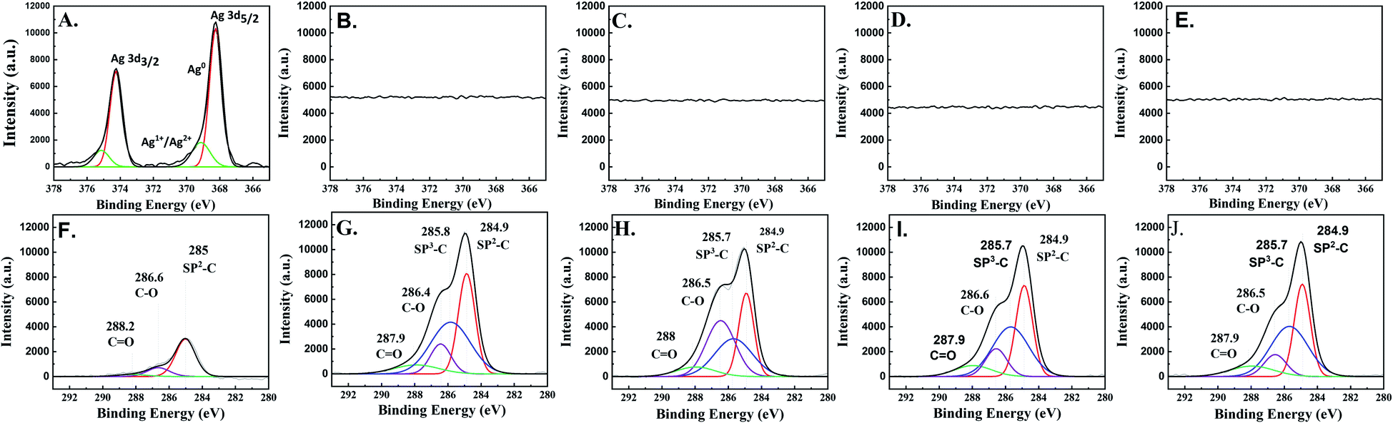 | ||
| Fig. 5 The XPS results of Ag 3d of the (A) Ag-electrocatalyst after CO2RR at ambient conditions for (B) 10, (C) 20, (D) 70, and (E) 140 min and C 1s of the Ag-electrocatalyst before (F) and after CO2RR at ambient conditions for (G) 10, (H) 20, (I) 70, and (J) 140 min. | ||
| Ag-10 | Ag-20 | Ag-70 | Ag-140 | |||||
|---|---|---|---|---|---|---|---|---|
| Center | Percentage [%] | Center | Percentage [%] | Center | Percentage [%] | Center | Percentage [%] | |
| sp2-C | 284.9 | 35.5 | 284.9 | 27.0 | 284.9 | 35.2 | 284.9 | 34.4 |
| sp3-C | 285.8 | 43.1 | 285.7 | 30.3 | 285.7 | 41.6 | 285.7 | 43.6 |
| C–O | 286.4 | 13.0 | 286.5 | 34.9 | 286.6 | 13.7 | 286.5 | 11.3 |
| CO |
287.9 | 8.4 | 288.0 | 7.9 | 287.9 | 9.5 | 287.9 | 10.7 |
The presence of a solid nanocrystalline carbon film on the Ag-electrocatalyst was further characterized by focused ion beam scanning electron microscopy with EDX (FIB-SEM-EDX) on the Ag-70 sample and the results are shown in Fig. 6. The sample was selectively ion milled using a focused ion beam with Ga ions. From the elemental mapping of the cross-section, deposition of carbon and Ag on the Cu substrate is evidently observed and the approximate thickness of the carbon film was determined to be around 2–3 μm. The SEM results of the cross-sectioned of the electrodes before and after CO2RR are shown in Fig. S1.† An increased in film thickness from 1.67 μm to 4.69 μm after CO2RR for 140 min was clearly observed.
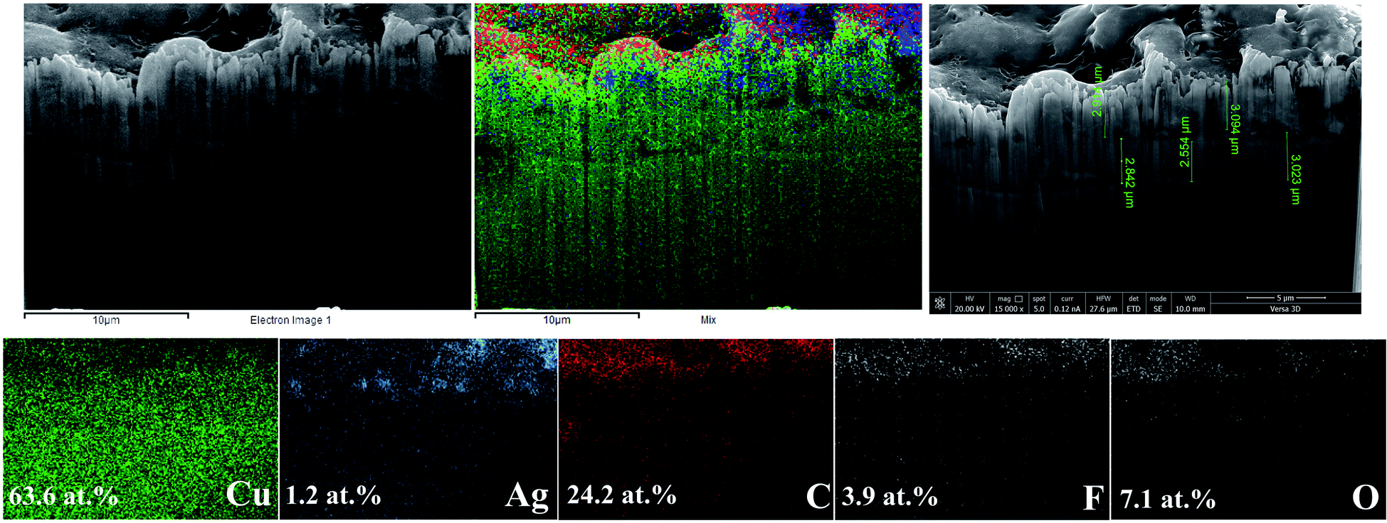 | ||
| Fig. 6 FIB-SEM images and elemental mapping of Ag-electrocatalyst after CO2RR at −1.6 V vs. Ag/Ag+ for 70 min. | ||
XANES spectra at the Ag L3-edge of the Ag-electrocatalysts before and after CO2RR were acquired in fluorescence mode (Fig. 7). The XANES spectrum of the Ag-electrocatalyst before CO2RR did not show the ultra-thin oxide layers because in the fluorescence mode, as the electron beam can penetrate the surface at the depth about 100–200 μm, i.e. much deeper than the XPS. Moreover, due to the electron beam penetrating over the approximate thickness of carbon layer, around 1 μm, XANES spectrum of Ag-electrocatalyst after CO2RR exhibited insignificant change on CO2RR.
 | ||
| Fig. 7 Normalized XANES spectra at Ag L3-edge of Ag-electrocatalyst before and after CO2RR for 10, 20, 30, 70, and 140, Ag foil, AgO, and Ag2O. | ||
The performance of the Ag-electrocatalysts for CO2RR for various reaction times in terms of CO2 conversion and product selectivity were analyzed based on the GC and NMR results. The CO2 conversion is depicted in Fig. S2.† The CO2 conversion decreased from 2.4% to around 1% when going from 10 min to 140 min on stream, which may be due to the solid carbon products covering the active Ag surface.30 The selectivity of products from CO2 is shown in Fig. 8. The selectivity of solid carbon from CO2 was nearly 100% (>94%) over the 140 min reaction time. CO was the only gaseous by-product detected by GC-TCD after 140 min with negligible amount at around 0.007 μmol. Determination of the faradaic efficiency of nanocrystalline carbon products is rather complicated because the exact moles of solid carbon formed could not be determined directly and the number of electrons involved in the CO2RR coupled growth of crystalline carbon are still unknown. Based on the GC results of gas products and the measured mass of the electrodes (before and after reaction), the faradaic efficiency of CO and Csolid from CO2RR-70 min were determined to be 0.028% and 273%, respectively. There could be other processes involving in the formation of nanocrystalline carbon products that can generate energy to drive reduction of CO into C such as the energy from C–C coupling reaction. The CO intermediates are firstly formed via the reduction of [BMIm]–carbene–CO2 intermediates using 2e− and then further reduced into Csolid.11 The 13C- and 1H-NMR analyses of the used electrolyte after CO2RR for various reaction times are shown in the ESI Fig. S3.† Comparing the spectra obtained after different times of the measurement, trace amount of 1,2-propanediol (1,2-PDO) was identified as the only liquid product. Although 1,2-PDO is not a typical major liquid product from CO2RR on either Cu or Ag electrocatalysts, the formation of diols including 1,2-PDO is possible on Ag-doped densely-arrayed Cu nanopyramids (Cu-DANs).31 The formation of diol products on Cu-DANs is promoted from three aspects: (1) improved CO* adsorption; (2) geometrically preferable sites for C–C coupling; and (3) boosted surface electron transfer. The confine space between adjacent nanopyramids has been shown to facilitate C–C coupling and retain the oxygen through O–Cu bond formation between the oxygen in the intermediates and copper on adjacent nanopyramids.32 In our study, the dendritic Ag grew into larger particles as the reaction time was prolonged and the reactivity of negatively Ag nanoclusters for CO2RR toward solid carbon would decrease. Under some certain conditions, it may render the confinement effect of Ag actives sites and Cu surface that promote the trimerization pathway of CO* moieties into 1,2-PDO. Nevertheless, the 1,2-PDO liquid product was produced in trace amount and was not included in the calculation of product selectivity. The weights of electrodes before and after reaction are also given in ESI S5.† The optical microscopy images (10×) of the Ag-electrocatalysts after CO2RR is shown in Fig. 9.
 | ||
| Fig. 8 Solid carbon product selectivity from CO2 (bar graph) and gaseous CO products (square symbol) after CO2RR for 10, 20, 30, 70, and 140 min. | ||
 | ||
| Fig. 9 The optical microscopy images (10×) of Ag-electrocatalyst after CO2RR for 10, 20, 30, 70, and 140 min. | ||
3.3 The evolution of nanostructure Ag–C formation from the ternary stage CO2RR (stage 3: amorphous carbon formation)
A long-term stability of the Ag electrocatalysts for CO2RR to nanostructure Ag–C products was investigated at −1.6 V vs. Ag/AgCl applied potential for 390 min time on stream. The geometric current density was calculated based on the electrode area. As seen from Fig. 10 (inset), the Ag-electrocatalyst was able to sustain a consistent current density of ∼7 mA cm−2 over 70 min of CO2RR. The current density started to swing between 5 and 12 mA cm−2 after 70 min time on stream, probably due to changes in the electrode surface. Nevertheless, the Ag-electrocatalysts were resistant to deactivation under the reaction conditions used. | ||
| Fig. 10 Total current densities of the Ag-electrocatalyst after CO2RR for 390 min. | ||
The characteristic Raman spectrum of Ag-390 is depicted in Fig. 11, exhibiting two main peaks with the dominant D-band and G-band, with ID/IG equal to 1.84. This observation reveals that over an extended period, most of the carbon products covering the Ag-electrocatalyst surface become amorphous. It is likely that there was insufficient energy to form crystalline nanostructured carbon due to partial coverage of the carbon products. Nevertheless, the Ag-electrocatalysts can maintain good stability for CO2RR during the extended reaction time. The solid carbon products were still observed after 390 min CO2RR, and CO was produced as a minor gaseous product of about 0.0009 μmol.
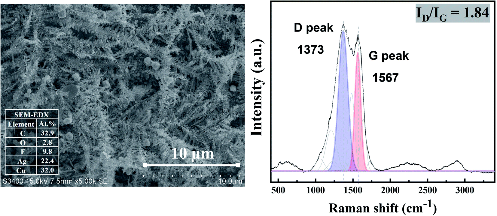 | ||
| Fig. 11 SEM images (Left column), and Raman results (Right column) of Ag-electrocatalyst after CO2RR at ambient conditions for 390 min. | ||
The evolution of Ag electrocatalysts and nanostructured carbon products, which simultaneously occur under the CO2RR environment at −1.6 V vs. Ag/AgCl applied potential (Scheme 1). Although the crystallization of the nanodiamond film on Ag nanocrystals takes place at room temperature and atmospheric pressure, the growth mechanism of the carbon is quite similar to the nucleation models proposed for the diamond CVD33 and to the diamond growth from organic compounds in hydrous fluids deep within the Earth, as recently reported by Frezzotti,34 in which diamond is produced under high temperature and/or high pressure. According to the well-known conventional CVD on Cu or Ni, the carbon source (gas, liquid, or solid) is decomposed at the high-temperature reaction zone and the carbon atoms are released and form carbon allotropes (mostly graphene).35 The nucleation and growth of graphene are dominated by surface diffusion of the decomposed carbon atoms.6 The present work emphasizes the importance of electric fields in significantly enhancing the crystallization process. Electric fields have been proven to be a valuable manipulation tool for controlling the crystallization process and the crystalline product. It can reduce the nucleation time, control the location of nucleation, crystal orientation, and polymorphism.36 A very recent work by Palyanov et al.37 has indicated that electric fields are key additional factor influencing diamond crystallization in the Earth lithospheric mantle. Moreover, referring to a previous study by Esrafilzadeh et al.,10 on the production of amorphous solid carbon at room temperature via CO2RR using liquid metals featuring atomically thin ceria interfaces, the liquid metal is highly conductive and is suitable for electrochemical redox processes. It has also been suggested that liquid metals can promote the formation of C–C bonds,10 and the flow characteristics of the liquid metal enhances the mass transfer on the electrolyte–electrode interface.38 Sun et al. recently showed that at room temperature “sub-10 nm” Ag particles can be deformed like a liquid droplet but remain highly crystalline in the interior.38 It can be rationalized that the negatively charged Ag metal nanoclusters may possess liquid-like surface properties, which could enhance both electrochemical reduction and C–C bonds formation.
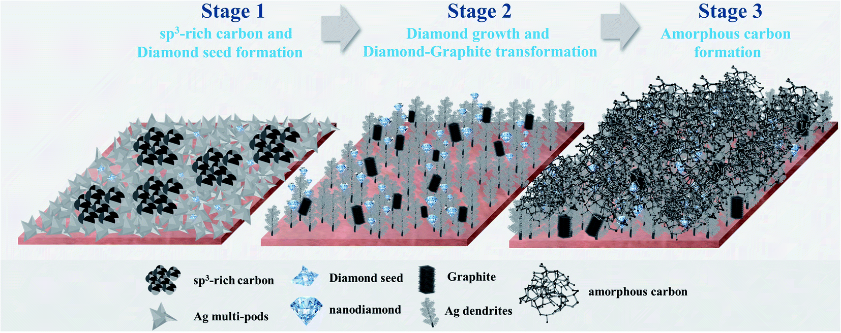 | ||
| Scheme 1 Evolution of nanostructured Ag-carbon films under room temperature CO2RR system. | ||
Within a 10 min reaction time, CO2 has already been reduced into single atom C* with the highest CO2 conversion and the highest solid carbon formation rate. However, probably due to the insufficient energy to continue the crystallization process to yield crystalline carbon products, only sp3 rich amorphous carbon was observed eventually. In the gas phase diamond synthesis, diamond nucleation occurs through metastable, hydrogen-terminated C groups acting as templates, before forming the sp3-structured C phase.39 In this work, when high energy electrons are transferred from the highly conductive Cu foil to the metal layers of the Ag nanocrystals and to the Ag oxides layers at the outermost layer of the electrode surface, the nascent Ag nanoclusters formed on the reduction and nanoclustering of the oxide layers could carry some energetic electrons and become highly active negatively charged Ag metal nanoclusters. It should be also mentioned that the nanocrystalline carbon products were generated on the tip of the structure where, the electric field is the highest.27 In the HF-CVD diamond process, diamonds also preferentially nucleate along scratches on the substrate or on the edge, owing to the high electric field gradient created by the electrons emitted from the hot filament.33 On further growth under electric field, the crystallization of carbon is significantly improved, as observed from the abrupt reduction of ID/IG of the carbon products when the reaction time increases from 10 min to 20 min. The Raman band corresponding to the diamond peak at 1332–1339 cm−1 is noticeable on the carbon products obtained after 30–140 min CO2RR. The Idiamond/IG increased from 0.64 to 0.78 when the reaction time was increased from 30 to 70 min, suggesting that diamond crystals continue to grow in this period under electric field. The highly energetic electron on the negatively charged metal nanoclusters, the high surface energy of sp3 bonded carbon, and the activation energy from C–C bonding acting as the driving forces.
As suggested in CVD diamond at low pressure, the diamond growth on a diamond seed is kinetically more favorable than graphite nucleation.33 However, once graphite is co-deposited, the growth rate of graphite is so much faster than that of diamond, the entire surface of diamond seeds would be covered with graphite and diamond cannot be grown any more. Thus, etching of graphitic surface layers is necessary to further the growth of diamond. For the nanocrystalline carbon growth from CO2RR at room temperature over Ag electrocatalysts in this study, both diamond and graphite phase are present after 70 min reaction time. According to the literature,21,40,41 in newly formed nano-sized diamonds, the high reactivity of surface carbon atoms could also enable the conversion of defective sp3-bonded carbon into graphitic or sp2–sp3 amorphous carbon surface domains. Besides, the detectable G + G′ peaks in the Raman spectrum of the Ag-70 at around 2950 cm−1 and the sp-bonded linear carbon peak at around 2144 cm−1 confirm the presence of sp-linear carbon intermediates on diamond-to-graphite transformation.22 At 140 min CO2RR, the growth of carbon allotropes is likely to be in the form of graphite and defective structures as the sp-bonded linear carbon peak disappeared and the peak at 2670 cm−1 was observed instead for the Ag-140 sample. The Idiamond/IG also drastically decreased from 0.78 (Ag-70) to 0.26 (Ag-140). The electric field and the total surface energy would gradually reduce as the coverage of solid carbon products on the Ag electrocatalysts increases, resulting in only amorphous carbon being formed eventually.
4. Conclusions
Structural transformation of Ag electrocatalysts and the nanostructured carbon allotropes formed on CO2RR at ambient conditions occurred simultaneously during the 10–390 min reaction time. The highest CO2 conversion and the highest solid carbon formation rate were observed at 10 min reaction time. At this stage (stage 1), reduction and nanoclustering of the ultra-thin Ag oxide layers into Ag nanocrystals with small dendritic structures and the reduction of CO2 into single atom C* took place, forming sp3 rich amorphous carbon, especially on the tip of the Ag particles, where the highest electric field is located. High energy was apparently created at the atomistic level of the catalytic sites of the metal electrodes under the imidazolium ionic-liquid aided CO2RR. Prolonging the reaction time to 20, 30, and 70 min, the crystallinity of the carbon products improved as the Ag dendrites grew larger. The TEM-EDX-SAED and the GI-XRD confirm the presence of nanodiamond crystallites and graphite at this stage. At last, the electric field and the total surface energy would gradually drop due to the coverage of solid carbon products on the Ag electrocatalysts, resulting in only amorphous carbon being formed. These findings can lead to design of nanostructured carbon and/or Ag/C products for future applications.Conflicts of interest
There are no conflicts to declare.Acknowledgements
The postdoctoral scholarship for S. W. from the Second Century Fund (C2F) Chulalongkorn University is gratefully acknowledged. The authors would like to thank the financial supports from the Malaysia-Thailand Joint Authority (MTJA) Research Cess Fund project, the Research Team Promotion grant (for J.P.) from the National Research Council of Thailand (NRCT), the JSPS Core-to-Core Program (Grant No. JPJSCCB20210004), the PMU-B e-Asia Joint Research Program, the CrystalLyte Co., Ltd., and the Soft Square International Co., Ltd.References
- J.-P. Tessonnier, D. Rosenthal, T. Hansen, C. Hess, M. E. Schuster, R. Blume, F. Girgsdies, N. Pfänder, O. Timpe, D. Su and R. Schlögl, Carbon, 2009, 47, 1779–1798 CrossRef CAS.
- P. S. Karthik, A. L. Himaja and S. P. Singh, Carbon Lett., 2014, 15(4), 219–237 CrossRef.
- R. Arriagada, G. Bello, R. García, F. Rodríguez-Reinoso and A. Sepúlveda-Escribano, Microporous Mesoporous Mater., 2005, 81, 161–167 CrossRef CAS.
- A. Rinaldi, B. Frank, D. S. Su, S. B. A. Hamid and R. Schlögl, Chem. Mater., 2011, 23, 926–928 CrossRef CAS.
- B. Deng, Z. Liu and H. Peng, Adv. Mater., 2019, 31, 1800996 CrossRef PubMed.
- C. Wang, K. Vinodgopal, G. Dai, Large-Area Synthesis and Growth Mechanism of Graphene by Chemical Vapor Deposition, in Chemical Vapor Deposition for Nanotechnology, 2018, IntechOpen, DOI:10.5772/intechopen.79959.
- N. Arora and N. N. Sharma, Diamond Relat. Mater., 2014, 50, 135–150 CrossRef CAS.
- M. Barberio and P. Antici, Sci. Rep., 2017, 7, 12009 CrossRef CAS PubMed.
- D. Dai, Y. Li and J. Fan, Carbon, 2021, 179, 133–141 CrossRef CAS.
- D. Esrafilzadeh, A. Zavabeti, R. Jalili, P. Atkin, J. Choi, B. J. Carey, R. Brkljača, A. P. O'Mullane, M. D. Dickey, D. L. Officer, D. R. MacFarlane, T. Daeneke and K. Kalantar-Zadeh, Nat. Commun., 2019, 10, 865 CrossRef.
- R. Nganglumpoon, S. Watmanee, T. Teerawatananond, P. Pinthong, K. Poolboon, N. Hongrutai, D. N. Tungasmita, S. Tungasmita, Y. Boonyongmaneerat, N. Jantaping, S. Wannapaiboon, P. Praserthdam, Y. Morikawa, J. G. Goodwin and J. Panpranot, Carbon, 2022, 187, 241–255 CrossRef CAS.
- Z.-Q. Cheng, Z.-W. Li, J.-H. Xu, R. Yao, Z.-L. Li, S. Liang, G.-L. Cheng, Y.-H. Zhou, X. Luo and J. Zhong, Nanoscale Res. Lett., 2019, 14, 89 CrossRef.
- Q. Zhou, S. Wang, N. Jia, L. Liu, J. Yang and Z. Jiang, Mater. Lett., 2006, 60, 3789–3792 CrossRef CAS.
- M. José-Yacamán, C. Gutierrez-Wing, M. Miki, D. Q. Yang, K. N. Piyakis and E. Sacher, J. Phys. Chem. B, 2005, 109, 9703–9711 CrossRef.
- Y. Yang, Y. Ping, Y. Gong, Z. Wang, Q. Fu and C. Pan, Prog. Nat. Sci.: Mater. Int., 2019, 29, 384–389 CrossRef CAS.
- A. A. Dubale, W.-N. Su, A. G. Tamirat, C.-J. Pan, B. A. Aragaw, H.-M. Chen, C.-H. Chen and B.-J. Hwang, J. Mater. Chem. A, 2014, 2, 18383–18397 RSC.
- J. Schwan, S. Ulrich, V. Batori, H. Ehrhardt and S. R. P. Silva, J. Appl. Phys., 1996, 80, 440–447 CrossRef CAS.
- A. Dychalska, P. Popielarski, W. Franków, K. Fabisiak, K. Paprocki and M. Szybowicz, Mater. Sci., 2015, 33, 799–805 CAS.
- P. K. Chu and L. Li, Mater. Chem. Phys., 2006, 96, 253–277 CrossRef CAS.
- S. Prawer, K. W. Nugent, D. N. Jamieson, J. O. Orwa, L. A. Bursill and J. L. Peng, Chem. Phys. Lett., 2000, 332, 93–97 CrossRef CAS.
- O. A. Shenderova and D. M. Gruen, Ultrananocrystalline Diamond: Synthesis, Properties and Applications, William Andrew, 2012 Search PubMed.
- E. O'Bannon, G. Xia, F. Shi, R. Wirth, A. King and L. Dobrzhinetskaya, Diamond Relat. Mater., 2020, 108, 107876 CrossRef.
- M. Yoshikawa, Y. Mori, H. Obata, M. Maegawa, G. I. Katagiri, H. Ishida and A. Ishitani, Appl. Phys. Lett., 1995, 67, 694–696 CrossRef CAS.
- A. Kaniyoor and S. Ramaprabhu, AIP Adv., 2012, 2, 032183 CrossRef.
- K. Ganesan, S. Ghosh, N. Gopala Krishna, S. Ilango, M. Kamruddin and A. K. Tyagi, Phys. Chem. Chem. Phys., 2016, 18, 22160–22167 RSC.
- D. Takagi, Y. Kobayashi and Y. Homma, J. Am. Chem. Soc., 2009, 131, 6922–6923 CrossRef CAS.
- M. Liu, Y. Pang, B. Zhang, P. De Luna, O. Voznyy, J. Xu, X. Zheng, C. T. Dinh, F. Fan, C. Cao, F. P. G. de Arquer, T. S. Safaei, A. Mepham, A. Klinkova, E. Kumacheva, T. Filleter, D. Sinton, S. O. Kelley and E. H. Sargent, Nature, 2016, 537, 382–386 CrossRef CAS PubMed.
- W. Oh, C. K. Rhee, J. W. Han and B. Shong, J. Phys. Chem. C, 2018, 122, 23084–23090 CrossRef CAS.
- A. M. Ferraria, A. P. Carapeto and A. M. Botelho do Rego, Vacuum, 2012, 86, 1988–1991 CrossRef CAS.
- N. Taccardi, M. Grabau, J. Debuschewitz, M. Distaso, M. Brandl, R. Hock, F. Maier, C. Papp, J. Erhard, C. Neiss, W. Peukert, A. Görling, H. P. Steinrück and P. Wasserscheid, Nat. Chem., 2017, 9, 862–867 CrossRef CAS PubMed.
- L. Chen, C. Tang, Y. Zheng, E. Skúlason and Y. Jiao, J. Mater. Chem. A, 2022, 10, 5998–6006 RSC.
- L. Chen, C. Tang, K. Davey, Y. Zheng, Y. Jiao and S.-Z. Qiao, Chem. Sci., 2021, 12, 8079–8087 RSC.
- N. M. Hwang, Non-Classical Crystallization of Thin Films and Nanostructures in CVD and PVD Processes, Springer, Dordrecht, 2016 Search PubMed.
- M. L. Frezzotti, Nat. Commun., 2019, 10, 4952 CrossRef PubMed.
- O. M. Dunens, K. J. MacKenzie and A. T. Harris, Environ. Sci. Technol., 2009, 43, 7889–7894 CrossRef CAS PubMed.
- L. F. Alexander and N. Radacsi, CrystEngComm, 2019, 21, 5014–5031 RSC.
- Y. N. Palyanov, Y. M. Borzdov, A. G. Sokol, Y. V. Bataleva, I. N. Kupriyanov, V. N. Reutsky, M. Wiedenbeck and N. V. Sobolev, Sci. Adv., 2021, 7, eabb4644 CrossRef CAS PubMed.
- J. Sun, L. He, Y.-C. Lo, T. Xu, H. Bi, L. Sun, Z. Zhang, S. X. Mao and J. Li, Nat. Mater., 2014, 13, 1007–1012 CrossRef CAS.
- M. A. Gebbie, H. Ishiwata, P. J. McQuade, V. Petrak, A. Taylor, C. Freiwald, J. E. Dahl, R. M. K. Carlson, A. A. Fokin, P. R. Schreiner, Z.-X. Shen, M. Nesladek and N. A. Melosh, Proc. Natl. Acad. Sci. U. S. A., 2018, 115, 8284–8289 CrossRef CAS PubMed.
- T. Petit, J.-C. Arnault, H. A. Girard, M. Sennour and P. Bergonzo, Phys. Rev. B: Condens. Matter Mater. Phys., 2011, 84, 233407 CrossRef.
- J. Cebik, J. K. McDonough, F. Peerally, R. Medrano, I. Neitzel, Y. Gogotsi and S. Osswald, Nanotechnology, 2013, 24, 205703 CrossRef PubMed.
Footnote |
| † Electronic supplementary information (ESI) available. See DOI: 10.1039/d1na00876e |
| This journal is © The Royal Society of Chemistry 2022 |