
Bulk halide perovskites as triplet sensitizers: progress and prospects in photon upconversion
Zachary A.
VanOrman
a,
Hayley K.
Drozdick
a,
Sarah
Wieghold
 abc and
Lea
Nienhaus
*a
abc and
Lea
Nienhaus
*a
aDepartment of Chemistry and Biochemistry, Florida State University, Tallahassee, FL 32306, USA. E-mail: lnienhaus@fsu.edu
bCenter for Nanoscale Materials, Argonne National Laboratory, Lemont, IL 60439, USA
cAdvanced Photon Source, Argonne National Laboratory, Lemont, IL 60439, USA
First published on 18th February 2021
Abstract
Triplet–triplet annihilation-based photon upconversion (TTA-UC) is a promising mechanism for harvesting lower energy photons by converting them to a higher energy. Photons generated from this process can be used for numerous applications, including photovoltaics, infrared sensing and imaging, biomedicine and photochemical reactions. Recently, bulk metal halide perovskite semiconductors have been introduced as triplet sensitizers for the TTA-UC process. While relatively efficient upconversion has been achieved at low fluences, the full potential of these materials as triplet sensitizers has not been unlocked. Here, we examine four pathways for device optimization and improvements, while discussing relevant works and potential further improvements. Finally, we discuss the outlook and bright future of such perovskite materials as triplet sensitizers and their important role in solid-state upconversion applications.
1. Introduction
Interest in bulk metal halide perovskite (MHP) materials has vastly increased in the past decade, as MHP materials have been examined as the active material in photovoltaic (PV) devices,1,2 lasing media,3,4 light-emitting diodes (LEDs),5 photocatalytic systems,6 among many other applications. Perhaps most notably, the external quantum efficiency of MHP PV materials has increased from 3.8% to 25.5% in just over a decade.7,8 MHP materials are made up of an ABX3 composition, where A is a monovalent cation, typically either small organic or alkali metal cations, such as methylammonium (MA), formamidinium (FA), or cesium. B is a divalent metal, typically either Pb or Sn, and X is a halide anion, such as Cl, Br, or I. The wide array of potential applications utilizing MHP materials originates from their unique and superior optoelectronic properties, including high optical absorption coefficients, optical tunability via simple changes in composition, solution processability, low exciton binding energies, large charge carrier diffusion lengths, and shallow defect sites, stemming from the electronic structure of the material. Recently, a novel application for MHP materials has emerged: triplet sensitizers for triplet–triplet annihilation based photon upconversion (TTA-UC).9–11The process of TTA occurs in certain polyaromatic hydrocarbons, where the result of an interaction between two spin-triplet states can result in the population of a singlet excited state.12–14 Direct optical excitation into a triplet excited state is forbidden due to spin selection rules, and therefore excitation of spin-triplet states commonly requires triplet sensitizer materials. Triplet sensitizers can come in a variety of forms: organometallics, where the triplet state is populated via intersystem crossing,14 semiconductor quantum dots (QDs), where the organic annihilator can be directly populated due to spin dephasing in the QD,15–17 direct singlet-to-triplet absorbing metal complexes, where the metal is commonly osmium, which is enabled by spin–orbit coupling,18,19 and bulk semiconductors, where asynchronous hole and electron transfer can occur from a sensitizer to an annihilator, reforming the exciton in the annihilator triplet state.20,21 MHP-sensitized TTA-UC falls in the latter category, where the annihilator is chosen to enable both energetically favorable hole and electron transfer, hence allowing for the population of the triplet state via charge transfer.
The triplet annihilator rubrene fits this requirement and has previously been shown to achieve efficient infrared-to-visible TTA-UC when coupled with a multitude of different triplet sensitizers.17,18,22 Due to its energetic alignment, where the triplet state is half the energy of the singlet state, rubrene is also capable of the reverse process of singlet fission. This has required the addition of dibenzotetraphenylperiflanthene (DBP) as a dopant to harvest the singlet states from rubrene via Förster resonance energy transfer (FRET) prior to their decay via singlet fission. The perovskite-sensitized UC scheme's overall energetic process, along with its components, is detailed in Fig. 1a. Upon absorption, an electron is promoted from the valence band to the conduction band (dotted black line) of the perovskite, leaving a hole behind. The electron can be transferred to the rubrene's triplet state, while the hole can be transferred to the highest occupied molecular orbital (HOMO) (solid black line). Once two rubrene triplet states are populated, TTA can occur (dashed orange line), resulting in the population of a singlet excited state in rubrene. The singlet is then harvested to DBP via FRET (solid orange line). Upon relaxation of the excited singlet state in DBP (dotted red line), the upconverted photon is emitted. This device design yields four primary areas of optimization of the UC device, shown in Fig. 1b: (i) the perovskite layer, (ii) the organic semiconductor (OSC) layer, comprised of rubrene and DBP, (iii) the interface between the perovskite and OSC layers, and (iv) the device fabrication methods. To optimize each component, mechanistic studies designed to understand each part of the UC device at the nanoscale are required.
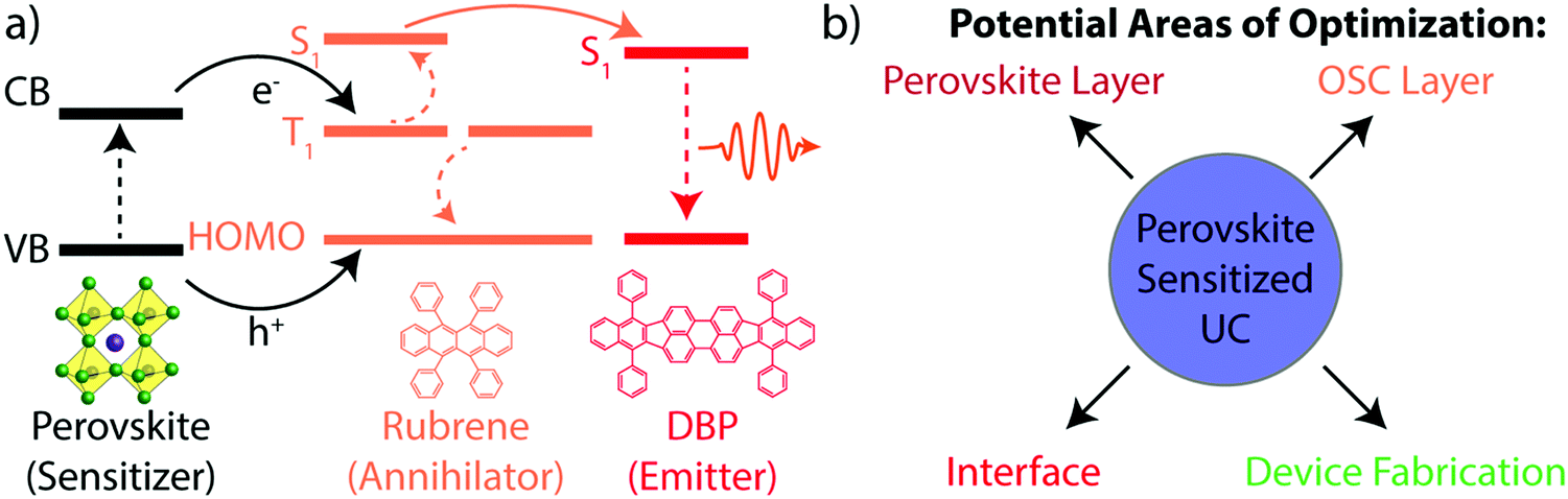 | ||
| Fig. 1 Perovskite sensitized TTA-UC. (a) Energetic scheme involving the perovskite (black), the rubrene triplet and singlet state (orange), and the DBP singlet state (red). (b) Potential areas of optimization of perovskite-sensitized UC devices. | ||
2. Bulk perovskite-sensitized TTA-UC
In this review, we aim to detail the studies on bulk perovskite-sensitized UC which have been undertaken by our group and others. Additionally, we will examine further work necessary to provide insight for each component, as well as an outlook for perovskite-sensitized UC in general.2.1 Perovskite layer
Bulk perovskite-sensitized solid-state TTA-UC was first introduced in concurrent works in 2019,20,21 although the perovskite compositions were slightly different. Nienhaus et al. utilized a MA0.15FA0.85PbI3 bulk perovskite film as the sensitizer material, along with an OSC layer comprised of rubrene doped with 1% DBP as the annihilator layer.20 The absorption and emission of the UC device components are shown in Fig. 2a, where the bulk emission of the perovskite is centered around ∼800 nm, and the OSC emission can be observed around 610 nm under 785 nm excitation, as a result of the UC process. The schematic in Fig. 2b further details this process. Additionally, the estimated absolute band energies of the perovskite valence and conduction bands are shown, along with the HOMO, lowest unoccupied molecular orbital (LUMO) and the triplet (T1) levels of rubrene. Direct electron transfer to the LUMO of rubrene is energetically unfavorable, although electron transfer to the triplet state and hole transfer to the HOMO are both energetically favorable. This is in contrast to the majority of quantum confined sensitizer/annihilator systems, where direct transfer of a bound exciton to the triplet state of the annihilator is thought to commonly occur.16,17,23,24 However, due to exciton binding energies below kT at room temperature,25 free charge carriers are rapidly generated in the sensitizer layer. Subsequent free charge carrier injection from sensitizer to annihilator has also since been observed in quantum-confined systems as well.26,27 Nienhaus et al. also note that the upconversion efficiency, ηuc, is challenging to measure due to low absorbance at 785 nm, along with parasitic interference effects. The estimated ηuc is essentially then limited by the perovskite sensitizer absorbance, which is a problem that has also plagued PbS QD systems in the solid-state previously.16,28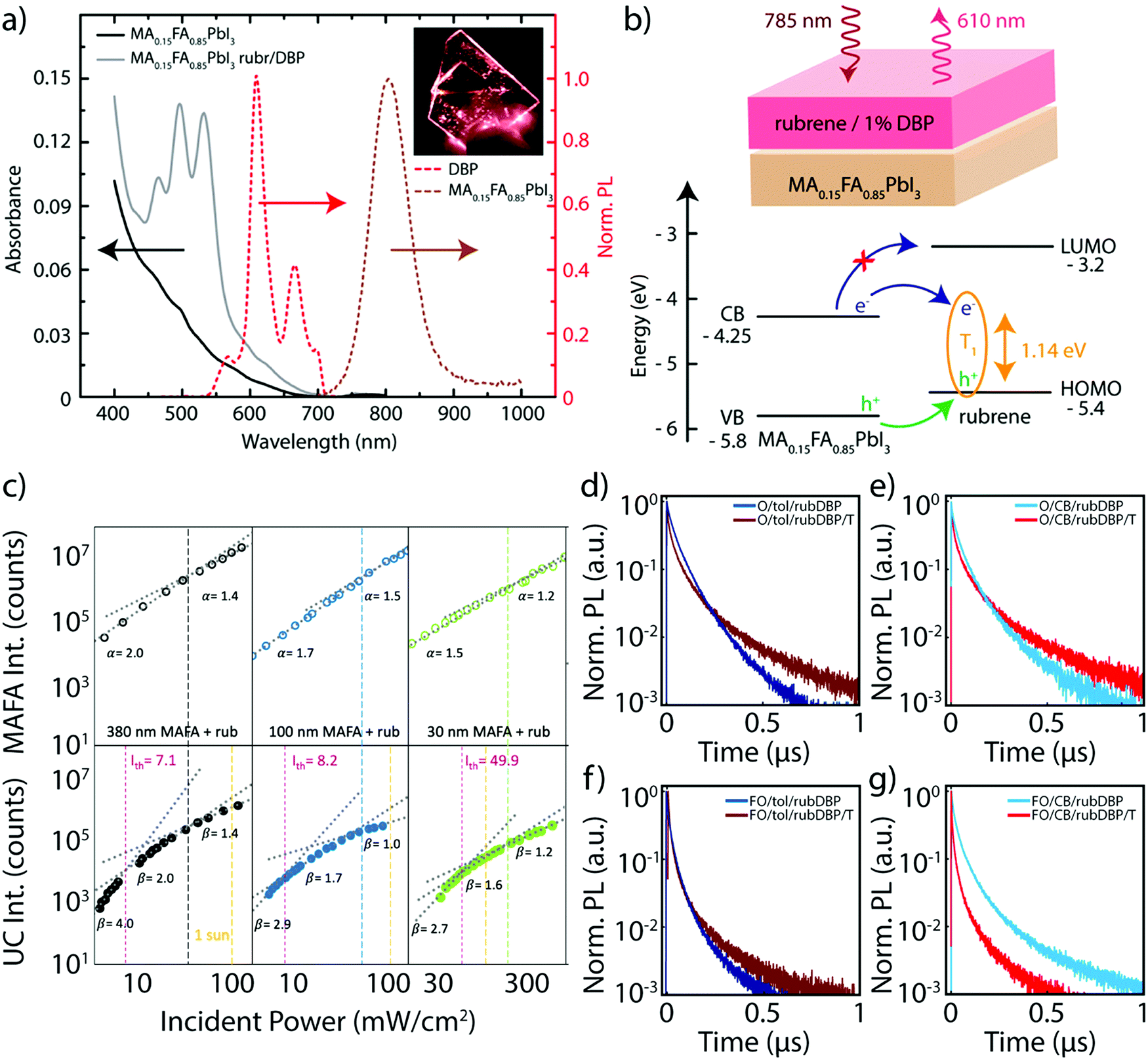 | ||
| Fig. 2 (a) The absorbance (solid) and normalized PL emission (dashed) of the perovskite only (black) and perovskite/OSC device (gray). The UC emission stemming from the OSC layer (red) and PL emission from the perovskite (brown) are both highlighted. The inset shows the device under 785 nm illumination. (b) A schematic of the device structure (top), where, upon 785 nm illumination, the OSC layer emits emission around 610 nm upon triplet sensitization via the perovskite layer. The rubrene triplet is occupied via sequential hole and electron transfer (bottom) from the perovskite valence and conduction band, respectively. Adapted with permission from ref. 20. Copyright 2019 American Chemical Society. (c) Emission intensity of the perovskite emission (top 3 panels) and the UC emission (bottom three panels) at various fluences. Adapted from ref. 21, Copyright 2019 Elsevier. (d–g) PL emission decay of the perovskite emission of MA-rich films fabricated with overstoichiometric PbI2 and either toluene (d) or chlorobenzene (e), and FA-rich films fabricated with overstoichiometric PbI2 and either toluene (f) or chlorobenzene (g). Adapted with permission from ref. 40. Copyright 2020 John Wiley and Sons. | ||
The limitation in perovskite film absorbance was investigated in-depth utilizing a different approach by Wieghold et al., where the thickness-dependence of the perovskite layer (MA0.85FA0.15PbI3) on the UC performance was studied.21 The result of the modulation of the perovskite thickness was investigated both through the emission from the perovskite layer and from the UC emission, occurring from the OSC layer at 780 nm excitation. Fig. 2c shows the power-dependent nature of the intensity of the perovskite emission (top) and the UC emission (bottom), as both were monitored for films of varying thickness. A quadratic to linear slope change in the UC photoluminescence (PL) intensity with increasing incident power density is characteristic of TTA-UC systems, stemming from the kinetics of the UC process.29–32 However, a slope change was also observed in the perovskite emission, which is most apparent in the thicker films. A super-linear region occurs at lower powers, which gives way to a linear regime. This is the result of a combination of non-geminate bimolecular recombination, trap filling, trap assisted recombination and band filling.33–36 Therefore, the underlying perovskite dynamics are further reflected in the UC emission, as evidenced in Fig. 2c. However, a clear trend is observed: the power threshold, Ith, which represents the point at which TTA-UC is efficient,29 decreases as the thickness of the perovskite film increases. This trend indicates a more efficient charge extraction process at higher perovskite thicknesses, which would result in the lower Ith values observed, along with an increase in the ηuc of the system. However, an increase in the perovskite thickness, in turn, also increases the likelihood of singlet back transfer and/or reabsorption of the upconverted light emitted from rubrene, meaning that there is a tradeoff in efficient charge extraction and ηuc of the device.
The perovskite's specific composition is also important, as the composition of the perovskite impacts the absolute band energies of the perovskite sensitizer material,37 which influences the energetic driving force of charge extraction to rubrene. Additionally, substituting FA for MA can lead to an increase of the thermal stability of the perovskite,38,39 as well as a decrease in the bandgap of the material, which could push the absorption further into the infrared, potentially allowing for an increase in the apparent anti-Stokes shift of the TTA-UC system. With this motivation, Bieber et al. monitored the charge extraction and UC performance of the two previously reported compositions: (i) the MA-rich composition of MA0.85FA0.15PbI3, and (ii) the FA-rich composition of FA0.85MA0.15PbI3.40 The PL decay lifetimes of the perovskite emission for MA-rich (denoted O/X/rubDBP) and the FA-rich (denoted FO/X/rubDBP) perovskites are shown in Fig. 2d–f. The early time quenching of the FA-rich perovskite as compared to the MA-rich perovskite emission is indicative of superior charge transfer from the perovskite layer to the OSC layer.
These trends were observed for films fabricated with either toluene and chlorobenzene (denoted as either tol or CB, respectively). Additionally, the devices fabricated with FA-rich compositions emitted UC light at higher intensities than the MA-rich compositions, again showing the importance of the perovskite composition on UC performance. Therefore, in future UC devices utilizing bulk perovskite sensitization, the perovskite composition should be chosen to maximize both the performance of the perovskite layer itself, but also tuned to maximize efficient charge extraction to the OSC layer, which in turn helps to maximize the UC performance of the device as a whole.
2.2 OSC Layer
While the initial excitation and free-charge carrier generation occur in the perovskite layer, TTA and the resulting upconverted emission occur in the OSC thin-film layer of the perovskite sensitized TTA-UC devices. In order for TTA to occur, the OSC layer must contain a triplet acceptor/annihilator molecule capable of annihilating the accepted triplets via TTA. Requirements for an efficient triplet annihilator are as follows: (i) the annihilator must have the proper energetics to allow for efficient triplet population from the triplet sensitizer, (ii) the annihilator should be readily able to annihilate two triplet states into a spin-singlet state, and (iii) the annihilator should have a high emission quantum yield from its singlet state, all to maximize the efficiency of the UC process. As previously mentioned, when paired with perovskite triplet sensitizers, the rubrene triplet annihilator must have proper alignment to both the valence and conduction bands in order to allow for hole and electron transfer. Rubrene has previously been used in multiple UC schemes, paired with both nanocrystal and metal–organic triplet sensitizers.16,17,22,41 Wieghold et al. demonstrated the importance of triplet diffusion to the TTA-UC process by monitoring the UC process at various fluences and mechanical modulation.42 Specifically, the UCPL decay lifetime was monitored as well as the UC emission intensity. Fig. 3a shows a representation of the UCPL decay for the perovskite sensitized TTA-UC device, where three regimes are observed – an initial fast rise, a slow rise, and a slow decay. The UCPL dynamics of a perovskite/OSC device under pulsed excitation at 4 μW (black), 2 μW (purple), and 4 μW modulated with an optical chopper (gray) are shown in Fig. 3a and b. Clearly shown in Fig. 3b are differences in the UCPL dynamics under the different conditions. Namely, the film under 4 μW illumination features a faster initial rise, while also having a higher magnitude of the initial rise. The film under chopped excitation, however, has a much more gradual rise before decaying. The differences in the UCPL dynamics are best described by the schematics in Fig. 3c and d. At high, unmodulated fluences, triplet excitons are rapidly formed near the perovskite/OSC interface, allowing for rapid TTA, as detailed in Fig. 3c. As this process occurs near the interface, the probability for back transfer to the perovskite layer increases. Fig. 3d shows the second case, where the triplet population is allowed to relax, most similarly to the chopped excitation source. Here, the triplet excitons diffuse far from the interface to find a triplet “partner” to undergo TTA with. As the diffusion takes the triplets farther from the interface, the efficiency of the UC process should increase, as the probability of parasitic singlet back transfer decreases. The two rise times in the UCPL lifetime reflect these two scenarios, while also showing the inherent sensitivity of perovskite sensitized TTA-UC devices to measurement conditions such as laser fluence and time after illumination.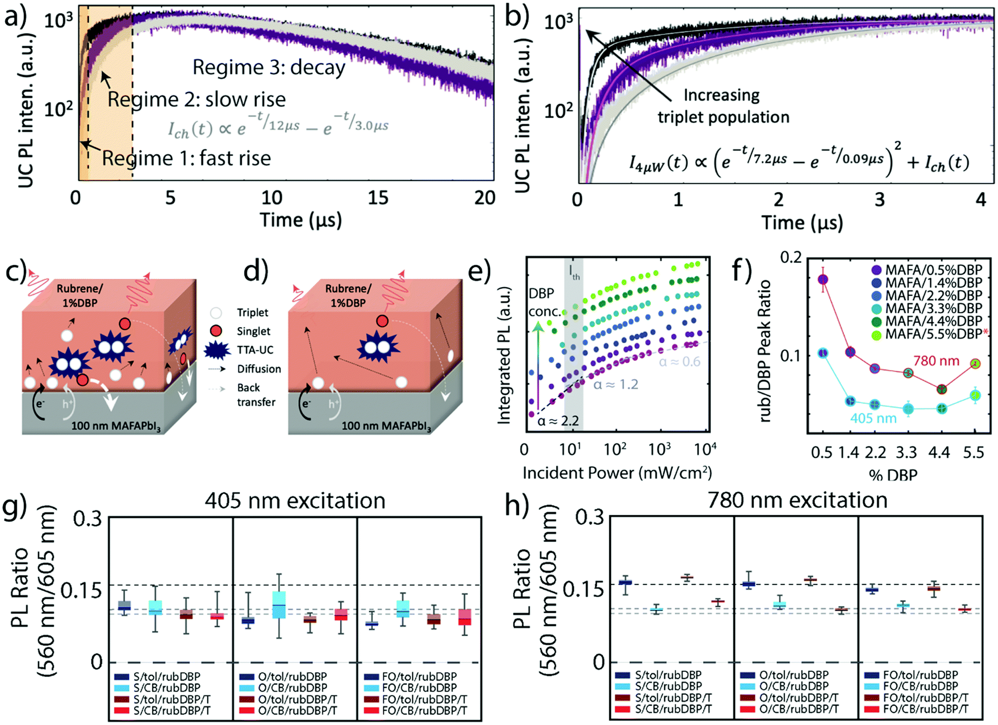 | ||
| Fig. 3 (a) A representative UCPL lifetime, where the two orange regions are different regimes of initial rises in intensity, and regime 3 is a slow decay. (b) and (c) UCPL lifetimes of a perovskite/OSC film under 4 μW pulsed excitation (black), 2 μW pulsed excitation (purple), and 4 μW pulsed excitation modulated by a chopper at a 50% duty cycle (gray). (c) Dynamics in the first 4 μs. (d) and (e) Schematics of TTA where the triplet population is high, resulting in TTA-UC close to the interface (d) and where the triplet population is low, resulting in TTA-UC far from the interface as a result of triplet diffusion (e). Adapted with permission from ref. 42. Copyright 2019 American Chemical Society. (f) The UCPL intensity as a function of the incident power of films made with perovskite and rubrene only (magenta, bottom) and various amounts of DBP doped (increasing from purple to light green). The Ith, where the slope changes from ∼2.2 to ∼1.2, is shown in gray. (g) The ratio of the first vibronic feature of rubrene and the first vibronic feature of DBP, at 405 nm excitation (blue circles) and 780 nm excitation (red circles) at various concentrations of DBP. Adapted with permission from ref. 43. Copyright 2020 American Chemical Society. (h) and (i) The ratio of the first vibronic feature of rubrene and the first vibronic feature of DBP under 405 nm excitation (h) and 780 nm excitation (i) for films fabricated under various conditions. Adapted with permission from ref. 40. Copyright 2020 John Wiley and Sons. | ||
The OSC layer can also be optimized by the modulation of the DBP dopant, which can impact the emission process. As previously stated, the OSC thin film layer of the perovskite sensitized device is composed of rubrene doped with DBP, commonly at a dopant concentration of 1%.21,42 As shown by Wu et al.,41 the introduction of DBP can improve TTA-UC when sensitized by PbS nanocrystals. However, we note that here the OSC layer was deposited via thermal deposition.
In a recent study by Nienhaus and coworkers, the influence of DBP doping in the OSC layer was investigated at various concentrations of DBP, where the OSC layer was deposited via solution-based spin coating.43 While the addition of higher concentrations of DBP changed the spectral shape of the emission and PL decay dynamics, Fig. 3e shows that the Ith remains largely unchanged, indicative of little to no change in the UC process as a whole as the percentage of DBP is increased (bottom to top). However, a difference in the films arises when compared under direct excitation at 405 nm and under 780 nm excitation, which results in UC emission. Fig. 3f shows the ratio of the first vibronic feature of rubrene (565 nm) and the first vibronic feature of DBP (605 nm) under both direct excitation (blue circles) and under 780 nm excitation (red circles) for the different DBP concentrations. As the emission from DBP takes place as a result of FRET, this ratio gives insight to the efficiency of this process. In both cases, the FRET efficiency from rubrene to DBP increases with the concentration of DBP, up to 4.4 wt%, reflected by the decrease in rubrene vibronic feature relative to DBP. We note that the films fabricated with 5.5 wt% DBP exhibited noticeable DBP aggregation, indicating that the resulting OSC is not representative of an even 5.5 wt% DBP doping level. However, the ratios are different at the two excitation wavelengths, meaning that different rubrene sub-populations are emitting depending on the excitation wavelength. Taken together, along with UCPL intensities that were fairly constant across the different concentrations of DBP, it was determined that DBP did not make a noticeable difference in the UC process, in contrast to previous reports of a 19-fold increase of the UC intensity upon DBP addition.41 This discrepancy was ascribed to differences in fabrication, as spin coating may result in more amorphous rubrene films (as compared to the polycrystalline film obtained by thermal evaporation), resulting in decreased amounts of singlet fission, potentially negating the benefit of DBP.44
Differences in the OSC layer were further investigated by Bieber et al.,40 who investigated the role of solvent by fabricating a variety of films using either toluene or chlorobenzene to dissolve the OSC components before deposition. The ratio of the vibronic features of rubrene and DBP were again compared under direct excitation at 405 nm and under 780 nm excitation, similar to earlier discussions.43Fig. 3g shows the ratio of rubrene/DBP emission under direct excitation. All films fabricated with toluene are denoted as X/tol/rubDBP where the films fabricated with chlorobenzene are denoted as X/CB/rubDBP. Within error, the ratio is similar in all films, ∼0.11. Fig. 3h shows the emission ratio of the same films, this time under 780 nm excitation. While the CB films show behavior similar to that observed under 405 nm excitation with a PL ratio of approximately 0.11, the toluene films demonstrate a higher PL ratio of approximately 0.16. The difference between the behavior under 405 and 780 nm excitation serves as further evidence of different molecules emitting under different excitation wavelengths when toluene is used as the solvent. Additionally, the differences between the two solvents can be explained by variations in the solubility and resulting packing of the OSC molecules upon deposition, which could impact the FRET process between rubrene and DBP.
2.3 Perovskite–OSC interface
Careful tuning of both the perovskite and OSC layers are crucial toward maximizing the efficiency of perovskite-sensitized TTA-UC devices, but the elucidation of the dynamics at the interface between the perovskite and OSC layers is also vastly important. The interface dynamics are especially magnified due to the nature of the charge transfer process, where two independent charge carriers must be transferred, in contrast to excitonic transfer in other TTA-UC schemes.9 Initial studies aimed at understanding either the perovskite layer, the OSC layer, or both built a level of fundamental knowledge, but the interface was first studied in depth by Wieghold and Nienhaus, who utilized a combination of organic molecules/perovskite pairings, along with various spectroscopic characterization techniques to probe the perovskite–OSC interface.45 Their main findings were two-fold. First, the presence of the OSC proved to passivate surface traps induced in the solution-processed fabrication method, which was manifested in longer lifetimes as compared to just MAFA/toluene films. This has been previously observed in perovskite solar cells, where rubrene has been utilized to passivate the perovskite surface.46,47 The source of the passivation was attributed to surface interactions between the perovskite cations and the delocalized π-elections in rubrene. An additional previous study by Ji et al. has also shown an upward bending of the perovskite conduction band and a downward bending of the LUMO and HOMO in rubrene.48 The electronic structure at the interface can therefore result in a charge build-up at the interface, as described by the schematic in Fig. 4a, where hole transfer can occur in the dark, leading to the build-up of an electric field before illumination. This can be observed in a rapid ‘photobleach’ of the UCPL, reflected in the green trace (top) of Fig. 4b, where rapid TTA can occur upon illumination due to the build-up of charges at the interface. Perovskites are known to photobleach or photobrighten under constant illumination, so for comparison, the MAFA PL was investigated (bottom, gray trace), as it is known that the underlying perovskite properties influence the UC properties. While the perovskite indeed photobleaches, leading to the slow decay of the upconverted emission, there is no rapid decrease in the PL at early times, highlighting that the effect of the precharging is limited to the OSC layer.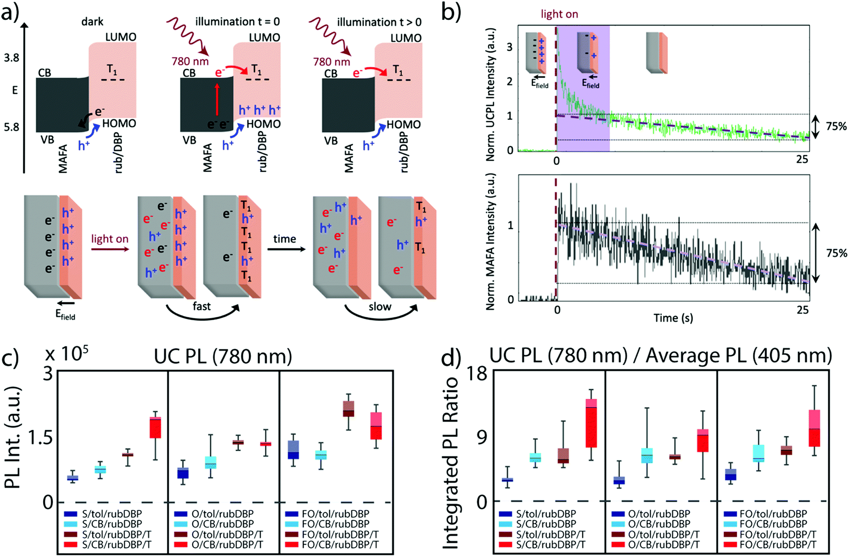 | ||
| Fig. 4 (a) Top: Band alignment of the perovskite (MAFA) and rubrene allow for hole transfer before illumination, resulting in a build-up of holes. Upon illumination, electron transfer occurs into the rubrene triplet state, and eventually, a steady-state occurs. Bottom: Schematic of the precharging effect described in (a), where UC occurs much faster after illumination and then eventually slows down after rapid TTA at the interface. (b) The UCPL (green) and perovskite emission (gray) over time, where the spike in the UCPL highlighted by the purple box occurs due to the build-up of charges at the interface, and then decreases. Adapted with permission from ref. 45. Copyright 2020 American Chemical Society. (c) and (d) Box plots detailing the UCPL intensity integrated from 500–700 nm (c) and the UCPL normalized by the PL under direct excitation at 405 nm for the various devices, where S, O, or FO denote stoichiometric PbI2 MA-rich, overstoichiometric PbI2 MA-rich, overstoichiometric PbI2 FA-rich devices respectively. Additionally, either toluene or chlorobenzene is used to fabricate the OSC layer (denoted as tol or CB, respectively), and the films annealed post-fabrication are denoted with a T. Adapted with permission from ref. 40. Copyright 2020 John Wiley and Sons. | ||
The effect of perovskite surface passivation was further probed by Bieber et al.,40 where “stoichiometric” and “overstoichiometric” amounts of PbI2 were added to fabricate the films, i.e., excess PbI2 was added to fabricate the overstoichiometric devices. Excess PbI2 has been previously observed to passivate defects at the perovskite surface and grain boundaries, potentially leading to higher power conversion efficiencies in solar cells.49–51Fig. 4c shows the integrated UCPL of the stoichiometric (films denoted with S) and overstoichiometric (films denoted with O) devices. Additionally, in Fig. 4d, the UCPL is normalized by the emission under direct excitation at 405 nm. Interestingly, no discernable difference is observed between the stoichiometric and overstoichiometric devices under similar fabrication methods. This likely stems from the passivation effects discussed earlier, as the perovskite surface is amply passivated by rubrene, which makes the excess addition of PbI2 redundant.
Further modifications of the solution-based fabrication method have direct impacts on the perovskite/rubrene interface. Namely, the antisolvent used in the deposition of the perovskite layer has definite impacts on the perovskite emission, charge extraction, and upconverted emission.52 Additionally, the specific method of deposition of the antisolvent and rubrene layer can affect the perovskite/rubrene interface.53 Although these changes impact the interface, they deal with modifications to the methods of device fabrication and will be discussed at length in Section 2.4.
2.4 Device fabrication
The brief yet rich history of research dedicated to MHP materials for the purpose of PV applications is an important source toward improvements in the fabrication of perovskite sensitized TTA devices. Antisolvent assisted perovskite fabrication is a common method for bulk perovskite growth, where an orthogonal solvent such as chlorobenzene or toluene is dropped simultaneously or soon after the deposition of a perovskite precursor. The antisolvent allows for rapid nucleation and fairly homogenous perovskite films.54–56 The choice of antisolvent is important for the fabrication of homogenous, well-passivated films in order to maximize the charge extraction to rubrene, maximizing the efficiency of the UC process. MacQueen and coworkers studied two different antisolvents, anisole and chlorobenzene, and their effects on the UC process as a whole.52 Although they observed negligible differences in the morphology of the perovskite surface and in the steady-state PL, the UCPL intensity of the anisole-treated film was roughly an order of magnitude higher. This discrepancy can be explained in part by the time-resolved perovskite PL emission. Fig. 5a and b show the perovskite PL transients for the anisole-treated and chlorobenzene-treated films, respectively. At low fluences, such as 45 nJ cm−2 (blue trace), nonradiative recombination-limited charge carrier dynamics can be probed. A direct comparison of the decay traces between the films treated with anisole and chlorobenzene yields a much longer charge carrier lifetime in the anisole treated films. This difference is attributed to shallow defect sites, which could affect the charge extraction process to rubrene. This result is in line with findings discussed earlier, where recombination due to surface trap states acts as a parasitic pathway toward efficient UC.21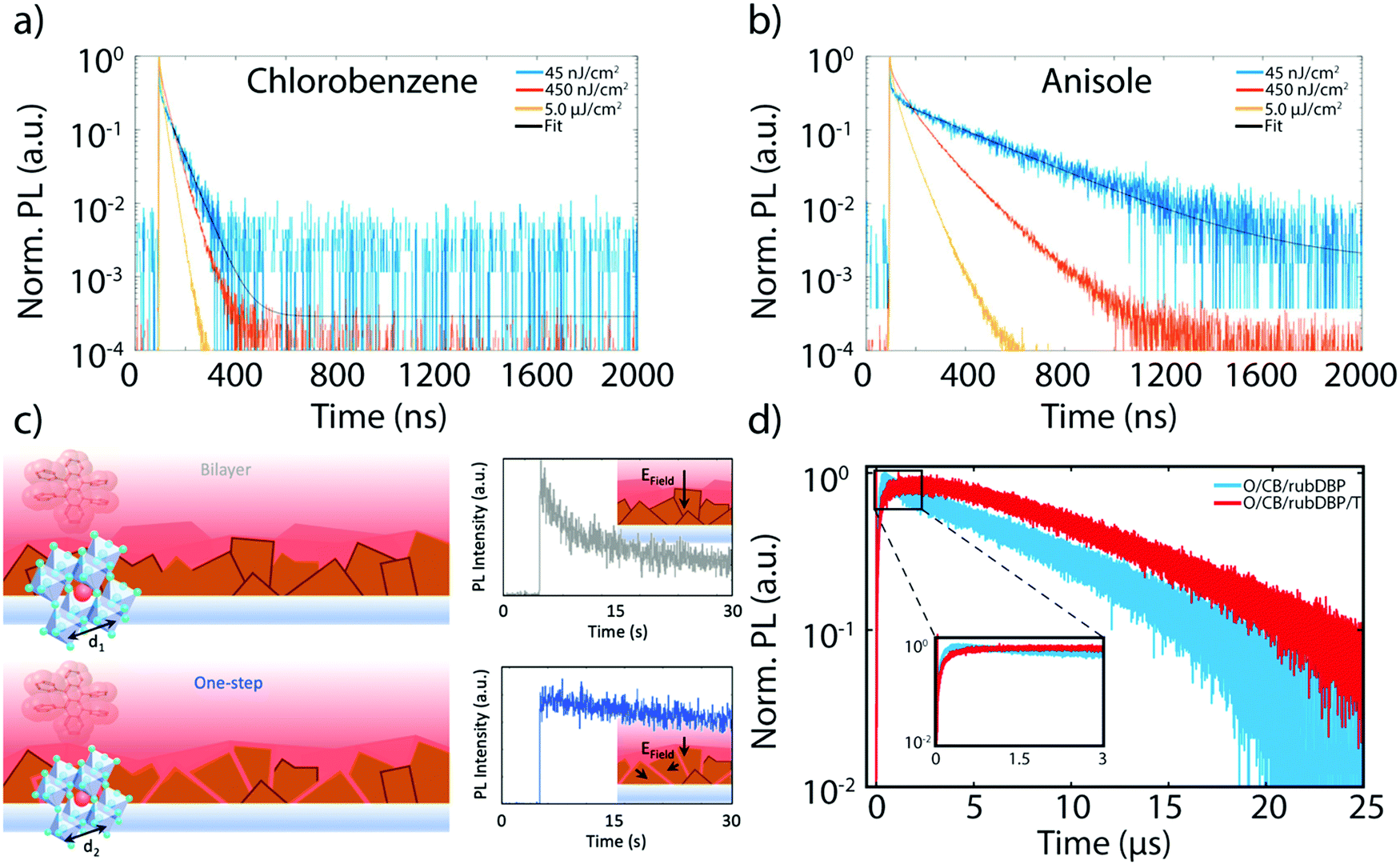 | ||
| Fig. 5 (a) and (b) Perovskite PL emission decay lifetimes of films fabricated treated with anisole (a) and chlorobenzene (b) at three different powers. The fit is denoted with a black line. Adapted with permission from ref. 52. Copyright 2020 John Wiley and Sons. (c) Schematic of the bilayer (top, left) and one-step (bottom, left) fabricated devices, along with the PL intensities of the bilayer (gray trace) and one-step (blue trace) fabricated device. The insets show the directionality of the electric field at the interface. Adapted from ref. 53 with permission. Copyright 2020 John Wiley and Sons. (d) Representative UCPL decay lifetimes of MA-rich films made with overstoichiometric PbI2 with (red) and without (blue) a post-fabrication thermal annealing step. Adapted from ref. 40 with permission. Copyright 2020 John Wiley and Sons. | ||
Further tuning of the fabrication method was probed by Nienhaus and coworkers,53 where TTA-UC devices were made by adding the OSC layer in situ during the antisolvent treatment process. This “one-step” method was then directly compared to devices made using the previous “two-step” method, where the rubrene is deposited after treatment with antisolvent. The findings, supported by additional optical and morphological characterization techniques, are summarized in Fig. 5c. In the two-step fabrication process, which results in a bilayer device (top left), the OSC layer coats the edges of the perovskite grains. However, in the devices fabricated using the one-step method (bottom left), the OSC can coat a larger area of the perovskite layer, allowing for a higher amount in charge extraction, as the interfacial area is much higher. This is further shown in the UCPL intensity over time, where the bilayer device shows a sharp initial decrease upon excitation (gray trace), and the one-step device does not have an initial spike in intensity (blue trace), as the electric field is minimized by differing orientations at the interface (inset). Furthermore, the one-step method simplifies the fabrication method, which could prove useful in eventual scaled-up device fabrication.
One of the most striking improvements in the UC performance was shown by Bieber et al.,40 where a post-fabrication thermal annealing process increased the UC intensity threefold. The improvements can be observed in the UCPL intensity in Fig. 4c and d, where for all devices, the UCPL intensity increases upon annealing (films that were annealed are denoted with a T at the end). Additionally, the UCPL decay dynamics of overstoichiometric films fabricated as normal (blue) and with the post-fabrication thermal annealing treatment (red) are shown in Fig. 5d. The device annealed post-fabrication exhibits a higher amount of diffusion mediated TTA-UC, as discussed previously, allowing for a higher ηuc. The improved UC performance of the annealed devices is attributed to a reforming process of the perovskite surface during the annealing, which improves the crystallinity of the perovskite layer, allowing for more efficient charge extraction due to the decrease in trap-assisted combination.
3. Summary and outlook
The vast improvements in TTA-UC sensitized via bulk MHP materials have come at a rapid pace, taking motivation in part from the wealth of literature dedicated to improving MHP materials for PV applications. As discussed here, recent studies and optimizations have focused on four main areas: improvements to the perovskite and OSC layers, elucidation of the perovskite/OSC interface, and improvements to the device fabrication process, which can have effects in one or many of the other three areas. To summarize, we have found that devices fabricated with the composition FA0.85MA0.15PbI3 with OSC layers deposited using chlorobenzene which are treated with a post-fabrication thermal annealing step featured the most intense UC emission. In addition, “one-step” deposition of the OSC layers simultaneous with the deposition of the antisolvent results in devices rivaling the performance of those fabricated by subsequent bilayer deposition, at a lower fabrication expenditure.Further advancements to these areas have the potential of yielding efficient upconverting devices for infrared light into visible light capable of being absorbed by a silicon solar cell, at a level high enough for eventual industrial relevance. Specifically, more attention should be devoted to the impact of OSC packing on the UC process. While it is clear that the packing of the OSC layer has an impact on the UC performance, it is unclear to what effect and how this knowledge can be used to maximize the ηuc of the device, or how the alignment of the organic layer can be tailored on the nanoscale. For example, functionalization of the components of the OSC layer could prove useful for this effect,57 or taking advantage of self-assembly to yield more reproducible OSC layers. Currently, only rubrene has been used as a triplet annihilator in conjunction with bulk perovskite sensitizers. However, any other triplet annihilator could be used provided the energetic requirements are met. This could include rubrene derivatives,57 or other polyaromatic hydrocarbons capable of TTA-UC. One advantage of rubrene over other triplet annihilators such as 9,10-diphenylanthracene (DPA), is the lack of aggregation induced issues such as excimer formation,58 which greatly reduces the efficiency of the UC process in the solid state. Therefore, if other triplet annihilators were to be used in place of rubrene, parasitic pathways, including the formation of excimers, should be investigated and limited.
Furthermore, MHP materials themselves offer unique challenges that will need to be overcome for industrial relevance, many of which are currently under study in the PV field. Specifically, the use of Pb is a concern, motivating the push for Pb-free perovskites,59–62 often through the substitution of Sn for Pb, which additionally causes a desired red-shift of the absorption onset. However, Sn-based perovskites are prone to oxidation, which is also problematic in terms of stability and performance.63,64 Additionally, the long-term stability of all MHP materials is an issue, as degradation of both the OSC and the perovskite layer could greatly decrease UC performance over time. In particular, it is well known that perovskite materials are prone to external stimuli65–68 including applied or internal electric fields, temperature, moisture or constant irradiation leading to ion migration and possible phase segregation.
While the perovskite-based UC devices discussed here have been shown to be stable over weeks to months, in contrast to previous PbS-based devices which have rapidly degraded within several days, more work needs to be done to understand the underlying causes of the degradation in the encapsulated samples. It would, therefore, be beneficial to observe specific results of the UC performance over time and under real-world conditions, e.g. under constant illumination or at slightly elevated temperatures due to the known increase in the solar cell temperature over the course of a day. In particular, it is known that perovskites photodarken or photobrighten under constant illumination, and we have been able to show that the underlying perovskite recombination properties influence the UC process due to a competition between trap-filling and triplet sensitization. Hence, it will be of great interest to observe the performance of the perovskite-based UC device under continuous illumination to simulate the conditions in a solar cell and observe the performance over time.
Baldo and co-workers have shown success in further boosting the UC performance of PbS-based devices by field-enhancement due to back-reflectors and the use of Fabry–Pérot microcavities.69,70 Further engineering of the device structure and fine-tuning of the synthetic conditions of the perovskite-based UC devices will be required to harness their full potential.
With respect to their fabrication, an additional drawback of the solution-processing approach used for these perovskite-based UC devices is an inherent difficulty in exact reproducibility. It is known that minor environmental changes can result in large changes in the quality of the obtained perovskite quality and resulting devices, and a fundamental knowledge of the cause is still lacking. While MacQueen and co-workers52 have contributed to the question of how fabrication influences the device performance, this is only the first of many steps required to fully grasp the underlying mechanisms.
While perovskite-sensitized TTA-UC devices have already been shown to be readily able to upconvert near infrared-to-visible light, they still are in their infancy. However, the potential of applying MHP materials as triplet sensitizers is great, in part due to both the superior properties of the material, along with the immense attention they are receiving for other applications.
Conflicts of interest
The authors declare no competing financial interests.Acknowledgements
The authors gratefully acknowledge Florida State University startup funds, as well as a planning grant from the Council on Research and Creativity (CRC) at FSU. This work was performed in part at the Advanced Photon Source and the Center for Nanoscale Materials, U. S. Department of Energy Office of Science User Facilities, and supported by the U. S. Department of Energy, Office of Science, under Contract No. DE-AC02-06CH11357.References
-
N.-G. Park, M. Grätzel and T. Miyasaka, Organic-Inorganic Halide Perovskite Photovoltaics: From Fundamentals to Device Architectures, Springer, 2016 Search PubMed
.
- H. J. Snaith, Nat. Mater., 2018, 17, 372–376 CrossRef CAS
- B. R. Sutherland and E. H. Sargent, Nat. Photonics, 2016, 10, 295–302 CrossRef CAS
- Q. Zhang, R. Su, W. Du, X. Liu, L. Zhao, S. T. Ha and Q. Xiong, Small Methods, 2017, 1, 1700163 CrossRef
- Z. Xiao, R. A. Kerner, L. Zhao, N. L. Tran, K. M. Lee, T.-W. Koh, G. D. Scholes and B. P. Rand, Nat. Photonics, 2017, 11, 108–115 CrossRef CAS
- B.-M. Bresolin, Y. Park and D. W. Bahnemann, Catalysts, 2020, 10, 709 CrossRef CAS
- A. Kojima, K. Teshima, Y. Shirai and T. Miyasaka, J. Am. Chem. Soc., 2009, 131, 6050–6051 CrossRef CAS
- NREL, Best Research-Cell Efficiencies, https://www.nrel.gov/pv/assets/pdfs/best-reserch-cell-efficiencies.20190411.pdf, accessed April 15, 2019.
- Z. A. VanOrman, A. S. Bieber, S. Wieghold and L. Nienhaus, MRS Commun., 2019, 9, 924–935 CrossRef CAS
- S. Wieghold and L. Nienhaus, PLoS One, 2020, 15, e0230299 CrossRef CAS
- S. Wieghold, Z. A. VanOrman and L. Nienhaus, Adv. Optical Mater., 2020, 2001470, DOI:10.1002/adom.202001470
- C. A. Parker, C. G. Hatchard and E. J. Bowen, Proc. R. Soc. London, Ser. A, 1962, 269, 574–584 Search PubMed
- J. Saltiel, G. R. March, W. K. Smothers, S. A. Stout and J. L. Charlton, J. Am. Chem. Soc., 1981, 103, 7159–7164 CrossRef CAS
- T. N. Singh-Rachford and F. N. Castellano, Coord. Chem. Rev., 2010, 254, 2560–2573 CrossRef CAS
- J. Kim, C. Y. Wong and G. D. Scholes, Acc. Chem. Res., 2009, 42, 1037–1046 CrossRef CAS
- L. Nienhaus, M. Wu, V. Bulović, M. A. Baldo and M. G. Bawendi, Dalton Trans., 2018, 47, 8509–8516 RSC
- Z. Huang, X. Li, M. Mahboub, K. M. Hanson, V. M. Nichols, H. Le, M. L. Tang and C. J. Bardeen, Nano Lett., 2015, 15, 5552–5557 CrossRef CAS
- S. Amemori, Y. Sasaki, N. Yanai and N. Kimizuka, J. Am. Chem. Soc., 2016, 138, 8702–8705 CrossRef CAS
- N. Yanai and N. Kimizuka, Acc. Chem. Res., 2017, 50, 2487–2495 CrossRef CAS
- L. Nienhaus, J.-P. Correa-Baena, S. Wieghold, M. Einzinger, T.-A. Lin, K. E. Shulenberger, N. D. Klein, M. Wu, V. Bulović, T. Buonassisi, M. A. Baldo and M. G. Bawendi, ACS Energy Lett., 2019, 4, 888–895 CrossRef CAS
- S. Wieghold, A. S. Bieber, Z. A. VanOrman, L. Daley, M. Leger, J.-P. Correa-Baena and L. Nienhaus, Matter, 2019, 1, 705–719 CrossRef
- T. N. Singh-Rachford and F. N. Castellano, J. Phys. Chem. A, 2008, 112, 3550–3556 CrossRef CAS
- K. Mase, K. Okumura, N. Yanai and N. Kimizuka, Chem. Commun., 2017, 53, 8261–8264 RSC
- X. Luo, R. Lai, Y. Li, Y. Han, G. Liang, X. Liu, T. Ding, J. Wang and K. Wu, J. Am. Chem. Soc., 2019, 141, 4186–4190 CrossRef CAS
- C. S. Ponseca, T. J. Savenije, M. Abdellah, K. Zheng, A. Yartsev, T. Pascher, T. Harlang, P. Chabera, T. Pullerits, A. Stepanov, J.-P. Wolf and V. Sundström, J. Am. Chem. Soc., 2014, 136, 5189–5192 CrossRef CAS
- X. Luo, Y. Han, Z. Chen, Y. Li, G. Liang, X. Liu, T. Ding, C. Nie, M. Wang, F. N. Castellano and K. Wu, Nat. Commun., 2020, 11, 1–10 Search PubMed
- X. Luo, G. Liang, Y. Han, Y. Li, T. Ding, S. He, X. Liu and K. Wu, J. Am. Chem. Soc., 2020, 142, 11270–11278 CrossRef CAS
- N. Geva, L. Nienhaus, M. Wu, V. Bulovic, M. A. Baldo, T. V. Voorhis and M. G. Bawendi, J. Phys. Chem. Lett., 2019, 10, 3147–3152 CrossRef CAS
- A. Monguzzi, J. Mezyk, F. Scotognella, R. Tubino and F. Meinardi, Phys. Rev. B: Condens. Matter Mater. Phys., 2008, 78, 195112 CrossRef
- A. Monguzzi, R. Tubino, S. Hoseinkhani, M. Campione and F. Meinardi, Phys. Chem. Chem. Phys., 2012, 14, 4322–4332 RSC
- Y. Y. Cheng, T. Khoury, R. G. C. R. Clady, M. J. Y. Tayebjee, N. J. Ekins-Daukes, M. J. Crossley and T. W. Schmidt, Phys. Chem. Chem. Phys., 2009, 12, 66–71 RSC
- T. W. Schmidt and F. N. Castellano, J. Phys. Chem. Lett., 2014, 5, 4062–4072 CrossRef CAS
- J. M. Richter, M. Abdi-Jalebi, A. Sadhanala, M. Tabachnyk, J. P. H. Rivett, L. M. Pazos-Outón, K. C. Gödel, M. Price, F. Deschler and R. H. Friend, Nat. Commun., 2016, 7, 13941 CrossRef CAS
-
M. Cadelano, M. Saba, N. Sestu, V. Sarritzu, D. Marongiu, F. Chen, R. Piras, F. Quochi, A. Mura and G. Bongiovanni, Perovskite Materials - Synthesis, Characterisation, Properties, and Applications, 2016 Search PubMed
- S. D. Stranks, V. M. Burlakov, T. Leijtens, J. M. Ball, A. Goriely and H. J. Snaith, Phys. Rev. Appl., 2014, 2, 034007 CrossRef
- T. C. Sum and N. Mathews, Energy Environ. Sci., 2014, 7, 2518–2534 RSC
- C.-C. Chueh, C.-Z. Li and A. K.-Y. Jen, Energy Environ. Sci., 2015, 8, 1160–1189 RSC
- Y.-M. Xie, B. Yu, C. Ma, X. Xu, Y. Cheng, S. Yuan, Z.-K. Wang, H. T. Chandran, C.-S. Lee, L.-S. Liao and S.-W. Tsang, J. Mater. Chem. A, 2018, 6, 9081–9088 RSC
- G. E. Eperon, S. D. Stranks, C. Menelaou, M. B. Johnston, L. M. Herz and H. J. Snaith, Energy Environ. Sci., 2014, 7, 982–988 RSC
- A. S. Bieber, Z. A. VanOrman, S. Wieghold and L. Nienhaus, J. Chem. Phys., 2020, 153, 084703 CrossRef CAS
- M. Wu, D. N. Congreve, M. W. B. Wilson, J. Jean, N. Geva, M. Welborn, T. Van Voorhis, V. Bulović, M. G. Bawendi and M. A. Baldo, Nat. Photonics, 2016, 10, 31–34 CrossRef CAS
- S. Wieghold, A. S. Bieber, Z. A. VanOrman and L. Nienhaus, J. Phys. Chem. Lett., 2019, 10, 3806–3811 CrossRef CAS
- S. Wieghold, A. S. Bieber, Z. A. VanOrman, A. Rodriguez and L. Nienhaus, J. Phys. Chem. C, 2020, 124, 18132–18140 CrossRef CAS
- D. M. Finton, E. A. Wolf, V. S. Zoutenbier, K. A. Ward and I. Biaggio, AIP Adv., 2019, 9, 095027 CrossRef
- S. Wieghold and L. Nienhaus, J. Phys. Chem. Lett., 2020, 11, 601–607 CrossRef CAS
- P. Qin, J. Zhang, G. Yang, X. Yu and G. Li, J. Mater. Chem. A, 2019, 7, 1824–1834 RSC
- D. Wei, F. Ma, R. Wang, S. Dou, P. Cui, H. Huang, J. Ji, E. Jia, X. Jia, S. Sajid, A. M. Elseman, L. Chu, Y. Li, B. Jiang, J. Qiao, Y. Yuan and M. Li, Adv. Mater., 2018, 30, 1707583 CrossRef
- G. Ji, G. Zheng, B. Zhao, F. Song, X. Zhang, K. Shen, Y. Yang, Y. Xiong, X. Gao, L. Cao and D.-C. Qi, Phys. Chem. Chem. Phys., 2017, 19, 6546–6553 RSC
- L. Wang, C. McCleese, A. Kovalsky, Y. Zhao and C. Burda, J. Am. Chem. Soc., 2014, 136, 12205–12208 CrossRef CAS
- J. Burschka, N. Pellet, S.-J. Moon, R. Humphry-Baker, P. Gao, M. K. Nazeeruddin and M. Grätzel, Nature, 2013, 499, 316–319 CrossRef CAS
- Y. C. Kim, N. J. Jeon, J. H. Noh, W. S. Yang, J. Seo, J. S. Yun, A. Ho-Baillie, S. Huang, M. A. Green, J. Seidel, T. K. Ahn and S. I. Seok, Adv. Energy Mater., 2016, 6, 1502104 CrossRef
- K. Prashanthan, B. Naydenov, K. Lips, E. Unger and R. W. MacQueen, J. Chem. Phys., 2020, 153, 164711 CrossRef CAS
- S. Wieghold, A. S. Bieber, J. Lackner, K. Nienhaus, G. U. Nienhaus and L. Nienhaus, ChemPhotoChem, 2020, 4, 704–712 CAS
- N. J. Jeon, J. H. Noh, Y. C. Kim, W. S. Yang, S. Ryu and S. I. Seok, Nat. Mater., 2014, 13, 897–903 CrossRef CAS
- M. Xiao, F. Huang, W. Huang, Y. Dkhissi, Y. Zhu, J. Etheridge, A. Gray-Weale, U. Bach, Y.-B. Cheng and L. Spiccia, Angew. Chem., Int. Ed., 2014, 53, 9898–9903 CrossRef CAS
- S. Paek, P. Schouwink, E. N. Athanasopoulou, K. T. Cho, G. Grancini, Y. Lee, Y. Zhang, F. Stellacci, M. K. Nazeeruddin and P. Gao, Chem. Mater., 2017, 29, 3490–3498 CrossRef CAS
- E. Radiunas, M. Dapkevičius, S. Raišys, S. Juršėnas, A. Jozeliūnaitė, T. Javorskis, U. Šinkevičiūtė, E. Orentas and K. Kazlauskas, Phys. Chem. Chem. Phys., 2020, 22, 7392–7403 RSC
- A. Nandi, B. Manna and R. Ghosh, Phys. Chem. Chem. Phys., 2019, 21, 11193–11202 RSC
- F. Hao, C. C. Stoumpos, D. H. Cao, R. P. H. Chang and M. G. Kanatzidis, Nat. Photonics, 2014, 8, 489–494 CrossRef CAS
- P. V. Kamat, J. Bisquert and J. Buriak, ACS Energy Lett., 2017, 2, 904–905 CrossRef CAS
- F. Giustino and H. J. Snaith, ACS Energy Lett., 2016, 1, 1233–1240 CrossRef CAS
- W. Ke and M. G. Kanatzidis, Nat. Commun., 2019, 10, 965 CrossRef
- N. K. Noel, S. D. Stranks, A. Abate, C. Wehrenfennig, S. Guarnera, A.-A. Haghighirad, A. Sadhanala, G. E. Eperon, S. K. Pathak, M. B. Johnston, A. Petrozza, L. M. Herz and H. J. Snaith, Energy Environ. Sci., 2014, 7, 3061–3068 RSC
- R. Prasanna, T. Leijtens, S. P. Dunfield, J. A. Raiford, E. J. Wolf, S. A. Swifter, J. Werner, G. E. Eperon, C. de Paula, A. F. Palmstrom, C. C. Boyd, M. F. A. M. van Hest, S. F. Bent, G. Teeter, J. J. Berry and M. D. McGehee, Nat. Energy, 2019, 4, 939–947 CrossRef CAS
- T. Xu, L. Chen, Z. Guo and T. Ma, Phys. Chem. Chem. Phys., 2016, 18, 27026–27050 RSC
- P. Holzhey and M. Saliba, J. Mater. Chem. A, 2018, 6, 21794–21808 RSC
- S. Wieghold, N. Shirato, V. Rose and L. Nienhaus, J. Appl. Phys., 2020, 128, 125303 CrossRef CAS
- S. Wieghold, A. S. Bieber, M. Mardani, T. Siegrist and L. Nienhaus, J. Mater. Chem. C, 2020, 8, 9714–9723 RSC
- M. Wu, J. Jean, V. Bulović and M. A. Baldo, Appl. Phys. Lett., 2017, 110, 211101 CrossRef
- M. Wu, T.-A. Lin, J. O. Tiepelt, V. Bulović and M. A. Baldo, Nano Lett., 2021, 21, 1011–1016 CrossRef CAS
| This journal is © The Royal Society of Chemistry 2021 |