
Two-dimensional multiferroics
Yunye
Gao
 a,
Mingyuan
Gao
ab and
Yuerui
Lu
*a
a,
Mingyuan
Gao
ab and
Yuerui
Lu
*a
aSchool of Engineering, College of Engineering and Computer Science, the Australian National University, Canberra, Australian Capital Territory 2601, Australia. E-mail: yuerui.lu@anu.edu.au
bCollege of Engineering and Technology, Southwest University, Chongqing 400716, China
First published on 11th November 2021
Abstract
Due to unprecedented application prospects such as high-density and low-power multistate storage, spintronics and nanoelectronics, two-dimensional (2D) multiferroics, coupled with at least two ferroic orders, have gotten a lot of interest in recent years. Multiple functions can be achieved in 2D multiferroics via coupling phenomena such as magnetoelectricity, piezoelectricity, and magnetoelasticity, which offers technical support for the creation of multifunctional devices. The research progress of 2D ferromagnetic–ferroelectric multiferroic materials, ferroelectric–ferroelastic multiferroic materials, and ferromagnetic–ferroelastic materials in recent years is reviewed in this paper. The categorization of 2D multiferroics is explored in terms of the multiple sources of ferroelectricity. The top-down approaches and the bottom-up methods used to fabricate 2D multiferroics materials are introduced. Finally, the authors outline potential research prospects and application scenarios for 2D multiferroic materials.
 Yunye Gao | Yunye Gao is a PhD candidate in the School of Engineering, College of Engineering and Computer Science at the Australian National University. She earned her BE degree from Zhejiang Normal University, China, in 2020. Her research interests include two-dimensional multiferroics and piezoelectric actuators. |
 Mingyuan Gao | Mingyuan Gao is an Associate Professor in the College of Engineering and Technology at Southwest University, China, and a Postdoctoral Researcher in the College of Engineering and Computer Science at the Australian National University. He earned his BE and ME degrees from Huazhong University of Science and Technology, China, in 2008 and 2010, respectively, and his PhD degree from Southwest Jiaotong University in 2018. He was a Senior Mechanical Engineer in Siemens AG from 2011 to 2018. His research interests include flexible electronics, energy harvesting, self-powered monitoring, and nonlinear dynamics. He won the 2010 GE Foundation TECH Award-First Place Award. |
 Yuerui Lu | Yuerui Lu is an Associate Professor in the College of Engineering and Computer Science at the Australian National University. He received his PhD degree from Cornell University, School of Electrical and Computer Engineering, in 2012. He holds a BS degree from the Department of Applied Physics at the University of Science and Technology of China. His research interests include MEMS/NEMS sensors and actuators, nano-manufacturing technologies, renewable energy harvesting, biomedical novel devices, nanomaterials, and nanoelectronics. He was the recipient of several awards, including the competitive ACT Young Tall Poppy of 2016, and the Media and Outreach Award from Australian National University in 2015. |
1. Introduction
Multiferroic materials, which are multifunctional materials with numerous main ferroic orders in a single phase, are fundamentally and technologically essential for a variety of applications, such as nonvolatile memory,1 sensors,2 energy harvesting,3 and actuators,4 among others.5–9 Ferroelectricity (FE), which breaks space-inversion symmetry, ferromagnetism (FM), which breaks time-reversal symmetry and ferroelasticity (FA), which breaks neither space-inversion symmetry nor time-reversal symmetry, are the well-known primary ferroic orders, which can be switched by their conjugate electric (E), magnetic (H), and stress (σ) fields, respectively. Ferrotoroidicity (FT), which breaks both the space-inversion and the time-reversal symmetry, should be switchable by crossed magnetic and electric fields, in addition to these three typical ferroic orders (Fig. 1(a)). Multiferroics exhibit unique properties due to mutual cross-coupling between ferroic orders via magnetoelectric, piezoelectric, or magnetoelastic interactions. In a ferromagnetic–ferroelectric multiferroic, an electric field can tune the magnetization and a magnetic field can tune the electric polarization; in a ferroelectric–ferroelastic multiferroic, stress fields can tune the electric polarization, and an electric field can tune the magnetization (Fig. 1(b)) This allows the design and assembly of numerous multipurpose devices to fulfil the conceivable and promising demands of individuals and industries. The ferromagnetic–ferroelectric multiferroic material, for example, allows for efficient writing and reading for high-density data storage while consuming minimal energy.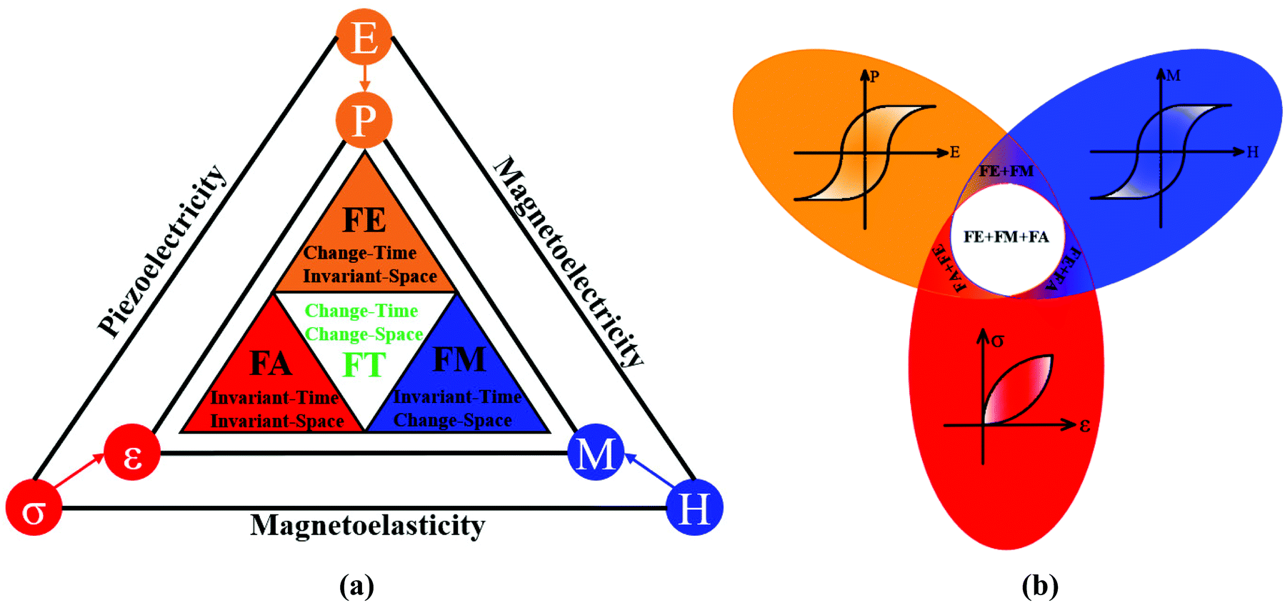 | ||
| Fig. 1 Different ferroic orders corresponding to the different time and space reversal symmetry and mutual cross-coupling between orders via magnetoelectric, piezoelectric, or magnetoelastic interactions. (a) FE breaking space-inversion symmetry; FM breaking time-reversal symmetry; FA breaking neither space-inversion symmetry nor time-reversal symmetry and FT breaking both space-inversion symmetry and time-reversal symmetry. (b) Mutual cross-coupling between ferroic orders. Redrawn based on ref. 25. | ||
However, most materials, particularly multiferroic materials, face significant technological challenges in terms of downsizing and integration, prompting scientists to seek out low-dimensional multiferroic materials of atomic thickness. Low-dimensional materials, as opposed to three-dimensional (3D) multiferroic materials, generally have smooth surfaces and high dielectric constants, making nanoscale devices possible. Since graphene was physically exfoliated from graphite in 2004,10 a wide range of 2D materials has been discovered and studied, including monochalcogenides,11,12 transition-metal phosphorus chalcogenides,13 phosphorene,5,14,15 molybdenum disulfide,16,17 transition-metal dichalcogenides,18–23 transition/rare-earth metal halides24 and so on.
In this paper, we discuss current research advances in 2D multiferroic materials over the last decade. We will look at the theoretical calculations and experimental discoveries of 2D multiferroics, as well as the categorization and preparation of 2D multiferroic materials, and future research possibilities for these materials.
2. Experimental and theoretical progress on 2D multiferroic materials
The past decade has witnessed remarkable progress in understanding of multiferroicity in 2D materials largely due to theoretical investigations based on DFT (first-principles density functional theory) and experimental observations.2.1 Research progress of 2D ferromagnetic–ferroelectric multiferroics
Due to the coexistence of the characteristics of the two-parent compounds and additional functions from the interaction between magnetic polarization and electrical polarization, multiferroic materials that are both ferroelectric and ferromagnetic may be more prevalent and diverse than traditional multiferroics, allowing for energy storage and efficient writing by an electric field. They are, however, uncommon for the following reasons: (1) ferroelectrics are insulators by definition, whereas itinerant ferromagnets require conduction electrons; (2) magnetism is typically caused by ordered spins of electrons in d/f orbitals partially filled by transition metals, whereas FE is frequently caused by residual polarization caused by stable off-centered ions with empty d/f orbitals. Ascher et al. reported the magnetoelectric coupling in bulk Ni3B7O13I for the first time in 1966.26 Following that, 2D multiferroic materials with magnetoelectric coupling effects, such as CrI3 with I vacancy,27 (TMPCs)-CuMP2X6 (M = Cr, V; X = S, Se),28 2D ferromagnets MXene, VS2 and MoN2,11 monolayer carbides and carbon nitrides (MXenes) Hf2VC2F2 monolayer,29 VOCl2 monolayer30 and other thin-film growth approaches have also been investigated. It is worth noting that VOI2 monolayer31,32 is either a ferroelectric magnet with spiral-spin configuration or a ferromagnetic metal, instead of a ferromagnetic–ferroelectric multiferroic, due to the presence of the heavy element iodine with a strong spin–orbit coupling, which produces an effective Dzyaloshinskii–Moriya interaction in a polar structure. Tu et al. published the first 2D organic multiferroics with coexisting ferromagnetic and ferroelectric characteristics in 2017, based on theoretical observation of the C6N8H organic network (Fig. 2(a)), allowing for the construction of a 2D multifunctional integrated circuit. Using DFT, monolayer transition metal phosphorus chalcogenides were confirmed to be 2D multiferroic semiconductors with strongly coupled ferroelectric and ferromagnetic orders in 2018, in which FM is caused by indirect exchange interaction between Cr/V atoms and FE is caused by copper atoms spontaneously moving away from the central atomic plane (Fig. 2(c)). These kinds of materials pave the way for 2D multiferroic switches and memories. Gao et al. in 2020 reported magnetoelectric coupling produced by Fe in a 2D BaTiO3(001) ultrathin film (see Fig. 2(b)), in which the Fe impurity enhances the overall magnetic moment but inhibits spontaneous polarization. This research suggests that by carefully replacing Ti atoms with Fe atoms, 2D BaTiO3 may be made into a multiferroic material. Zhong et al. explored a 2D thin-layer CuCrX2 (X = S or Se) multiferroic with the desired coexistence of FM and FE and high magnetoelectric coupling (Fig. 2(d)). Furthermore, the interlayer coupling parameter gradient between neighboring layers resulted in a variety of magnetoelectric layers of various thicknesses. It not only cleared the path for room-temperature ferromagnetic–ferroelectric multiferroicity with significant magnetoelectric coupling, but it also has the potential to spur additional study into multiferroicity in 2D systems.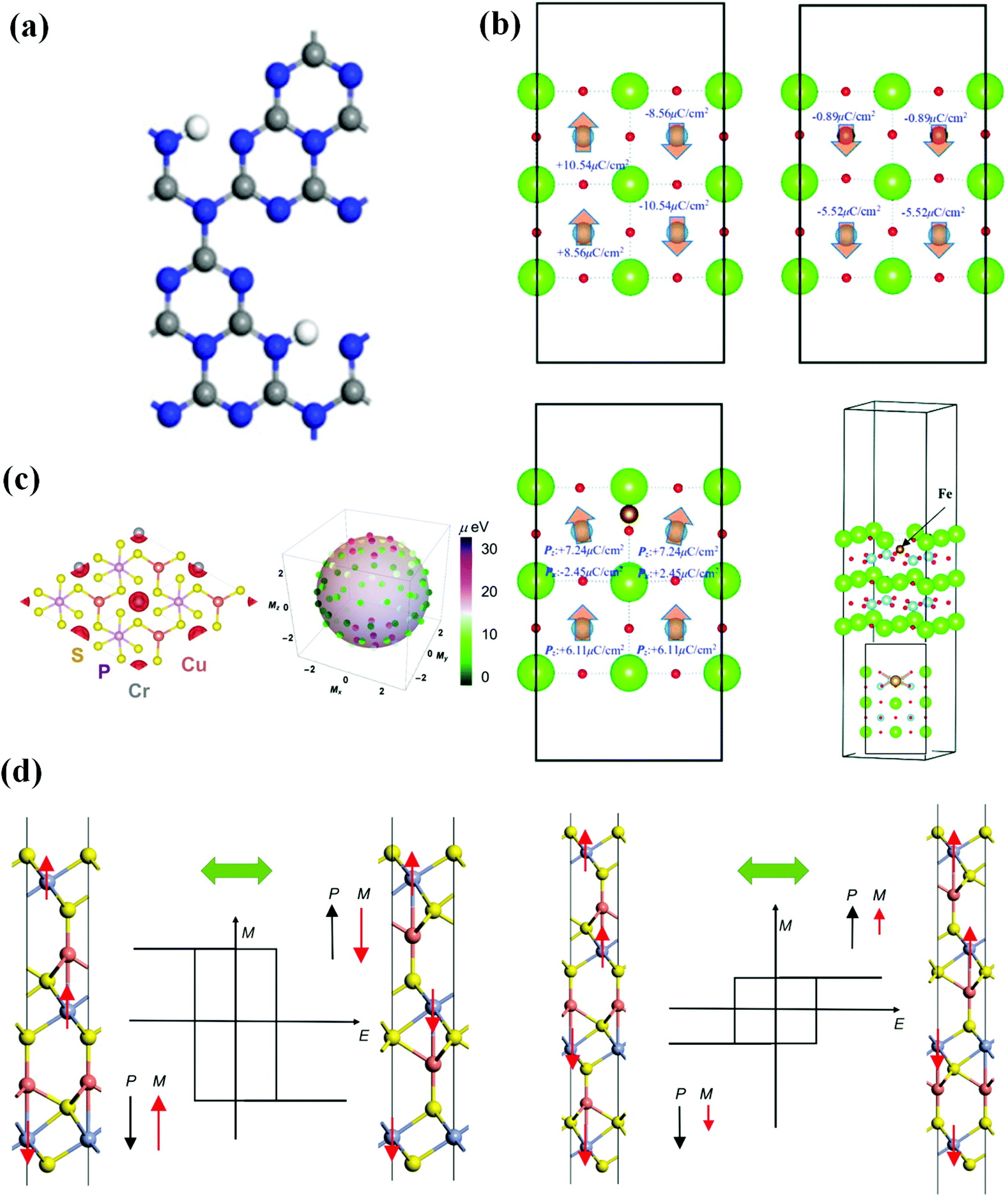 | ||
| Fig. 2 Several 2D ferromagnetic–ferroelectric multiferroic materials in recent years. (a) Optimized structure of C6N8H. Reproduced with permission.33 2017, American Chemical Society. (b) Ferroelectric characteristics of 2D BaTiO3 ultrathin film without and with Fe. Reproduced with permission.34 Copyright 2020, The Royal Society of Chemistry. (c) Ferroelectric and magnetic characteristics of monolayer CuCrP2S6. Reproduced with permission.35 Copyright 2018, AIP Publishing. (d) Geometric structures and multiferroic conversion of Cu2(CrS2)3 (left) and Cu3(CrS2)4 (right) thin films. Reproduced with permission.36 Copyright 2020, China Science Publishing & Media. | ||
2.2 Research progress of ferroelectric–ferroelastic multiferroics
Ferroelectric–ferroelastic multiferroics are a kind of 2D multiferroic material with strong spontaneous ferroelectric polarization and spontaneous ferroelastic lattice strain, which is thermodynamically stable at room temperature and higher and can be effectively controlled by elastic strain engineering. In 2017, Wang and Qian predicted that 2D monolayer group IV monochalcogenides MX (M = Ge, Sn and X = S, Se), are a class of 2D ferroelectric–ferroelastic multiferroics (Fig. 3(a)), which has the potential to become multifunctional equipment, including 2D ferroelastic memory, 2D ferroelectric memory, 2D ferroelectric excitonic photovoltaics, and 2D ferroelectric–ferroelastic nonvolatile photonic memory. In the same year, a group of researchers predicted the giant second harmonic (SHG)37,38 in the newly revealed 2D ferroelectric–ferroelastic multiferroic materials (group IV monochalcogenides) (Fig. 3(b)), which paved a range of new ways for multiferroic materials, nonlinear optoelectronics and 2D ferroelectrics, among other things. For example, by utilizing noncontact noninvasive optical SHG methods, it can achieve ultrafast optical characterization of local electronic and atomistic structures and active mechanical/optical/electrical switching of ferroic orders in 2D multiferroics. Wu and Zeng revealed, in 2017, that Bi2O2Se, Bi2O2S and Bi2O2Te (Fig. 3(c)), are multiferroics possessing FE and FA, which makes it possible to integrate the room temperature functional nonvolatile memories (NVM) into future nanocircuits. Besides, the good matching of the lattice constants of the bismuth oxychalcogenide makes the heterostructure devices have no lattice mismatch problems, to be tailored to the application. In 2017, a multiferroic material with linked FA and FE was anticipated for the Boron pentaphosphide (BP5) monolayer (Fig. 3(d)). The expected reversible strain is the highest among all ferroelastic materials (41.41%). In BP5, the spontaneous in-plane polarization is due to the difference in electronegativity between the phosphorus and boron atoms and the non-centrosymmetric structure. It has been proposed as a possible nanomaterial for the construction of optoelectronic or electromechanical devices, such as nonvolatile memory with easy read/write capabilities. Gao et al. revealed in 2019 that silver/copper mono-halides had linked FE and FA, as well as modest switching barriers (Fig. 3(e)). Using basic principles, Zhang et al. discovered in 2021 that bilayer ZrI2 (Fig. 3(f)) not only retains the in-plane and out-of-plane polarization caused by the redistribution of charges between layers but also has FA due to its crystal symmetry. It described a new design concept that achieves ferroelastic FE by using van der Waals interaction as a disturbance in a double-layer lattice. This approach provides a new way for 2D ferroelastic FE to be realized and developed.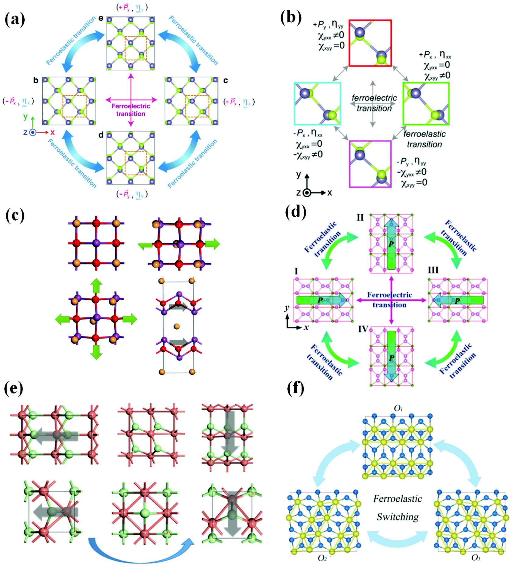 | ||
| Fig. 3 Several 2D ferroelectric–ferroelastic multiferroic materials in recent years. (a) Ferroelastic and ferroelectric transition of monolayer group IV monochalcogenides. Reproduced with permission.39 Copyright 2017, IOP Publishing. (b) Ferroelastic and ferroelectric transition of monolayer GeSe. Reproduced with permission.40 Copyright 2017, American Chemical Society. (c) Geometry of Bi2O2Se under uniaxial and biaxial strain. Reproduced with permission.41 Copyright 2017, American Chemical Society. (d) Ferroelastic and ferroelectric transition of BP5. Reproduced with permission.14 Copyright 2017, IOP Publishing. (e) Ferroelastic switching of 2D polymorphs of CuCl. Reproduced with permission.42 Copyright 2019, The Royal Society of Chemistry. (f) Ferroelastic switching of monolayer ZrI2. Reproduced with permission.43 Copyright 2021, American Physical Society. | ||
2.3 Research progress of ferromagnetic–ferroelastic multiferroics
Both ferromagnetic and ferroelastic orders could be found in ferromagnetic–ferroelectric multiferroics. Seixas et al. revealed in 2016 that depending on the hole density, the α-SnO monolayer (Fig. 4(a)) can be ferromagnetic, ferroelastic, or even multiferroic. In other words, a new class of multiferroic 2D systems is discovered in a range of hole densities where the material exhibits both FM and FA. These materials open up new avenues for developing flexible memory and integrating them with other flexible electronics. In 2020, Xu et al. suggested a new 2D multiferroic material (single-layer AgF2) as an antiferromagnetic ferroelastic semiconductor with high spin polarization (Fig. 4(b)). The presence of antiferromagneticity and FA in the AgF2 monolayer is important for the study of 2D multiferroics and makes it a viable platform for future multifunctional device applications. In 2020, Xu et al. reported that magnetic easy axes in 2D ferromagnets: CrSX (X = Br, I, Cl) monolayers could be switched by ferroelastic strain (Fig. 4(c)), showing that these monolayers are 2D multiferroic materials. By integrating ferroelastic phase transition, these discoveries give a potential framework for controlling spintronic characteristics. Pang et al. proposed in 2021 that 2D tetragonal structures XOBr (X = Ru, Tc) (Fig. 4(d)) are multiferroic semiconductors with significant electrical anisotropy, FA, and coexisting ferromagnetic characteristics. The ferroelastic switch may be used to modify the direction of anisotropic electron behaviour by applying external stress. The findings support the creation of electrical and memory devices that can be controlled.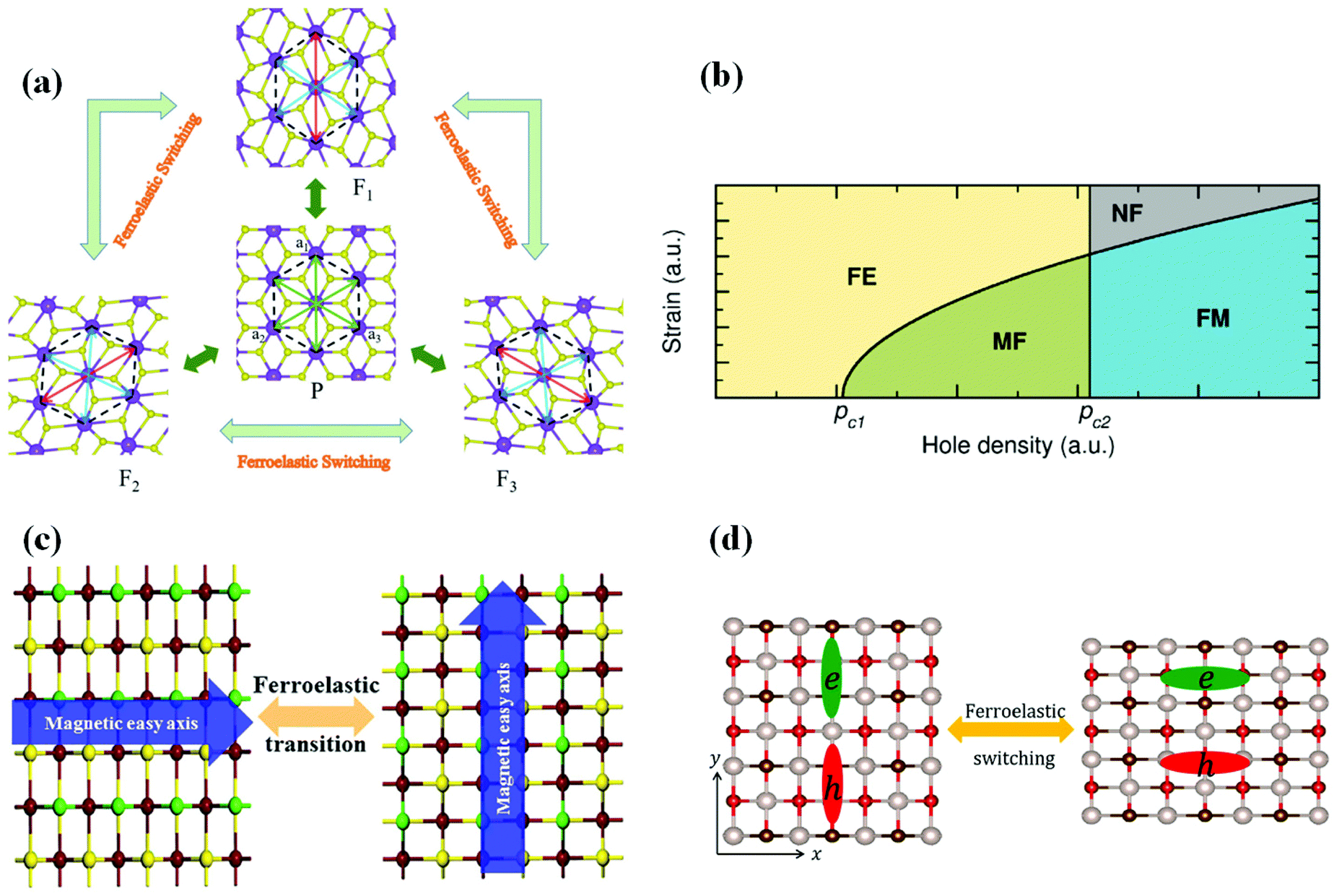 | ||
| Fig. 4 Several 2D ferromagnetic–ferroelastic multiferroic materials in recent years. (a) Ferroelastic switching of the monolayer AgF2. Reproduced with permission.44 Copyright 2020, The Royal Society of Chemistry. (b) Schematic diagram of the generalized Landau model in a multiferroic (FM and FA) α-SnO monolayer. Reproduced with permission.45 Copyright 2016, American Physical Society. (c) The ferroelastic transition of the CrSI monolayer. Reproduced with permission.46 Copyright 2020, AIP Publishing. (d) Ferroelastic switching of TcOBr. Reproduced with permission.47 Copyright 2020, Elsevier. | ||
In general, disclosed 2D multiferroics, whether ferromagnetic–ferroelectric, ferroelectric–ferroelastic, or ferromagnetic–ferroelastic, are extremely rare; the majority of them were postulated based on theoretical simulations, with little practical advances as far. More significantly, the vast majority of theoretically postulated multiferroic characteristics are type I; few materials have strong ferroic coupling. 2D multiferroic materials have yet to be used in practical applications. This intriguing but mostly unexplored field of study offers enormous possibilities for the academic community.
3. Classification of 2D multiferroics
3.1 Classification of multiferroics
There are two classification criteria for multiferroic materials: one is based on the coupling effect between the ferroic orders, namely, ferroelectric–ferromagnetic, ferromagnetic–ferroelastic, and ferroelectric–ferroelastic multiferroics corresponding to magnetoelectric, piezoelectric and magnetoelastic effect, respectively. The other is proposed by Khomskii in 2009 to divide multiferroics into two categories, i.e. type-I and type-II multiferroic materials48,49 (Fig. 5(a)). With regard to type-I multiferroics, the origins of FE and FM are different and the coupling between FE and magnetism is usually weak. According to current reports, type-I multiferroics are more common with large polarization and high transition temperatures. In contrast, type II multiferroic materials, in which FE only appears in a magnetically ordered state that breaks the inversion symmetry, are more attractive in applications due to the strong coupling between FE and magnetism.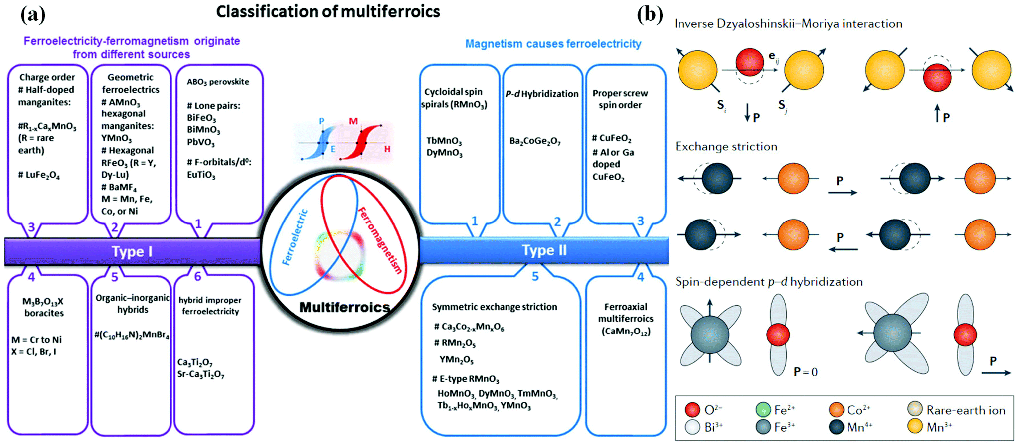 | ||
| Fig. 5 Microscopic mechanisms of FE in type-II 2D multiferroics. (a) The classification of the multiferroic materials into two types with subclass groups. Reproduced with permission.60 Copyright 2021, Springer Nature. (b) Three major microscopic mechanisms of FE in type-II multiferroic materials. Reproduced with permission.61 Copyright 2014, IOP Publishing. | ||
Typical multiferroics, BiFeO3,50 BiMnO351 and PbVO3,52 belong to the lone-pair category, where cations owing highly polarizable 6s2 lone-pair electrons (Bi3+ and Pb2+) play a major role in the origin of FE and have high polarizability.
Charge-ordered multiferroics are often observed in transition metal compounds with ions that formally have a mixed valence. Typically, site-centered charge order and bond-centered charge order are two general types, where mirror planes of the charge order structure can be marked at ions or bond centers. In order to realize FE in charge-ordered multiferroics, it is necessary to combine these two charge orders, namely, the existence of inequivalent sites and bonds in the system at the same time. Some systems like an organic ferroelectric (TMTTF)2X53 or multiferroic LuFe2O4![[thin space (1/6-em)]](https://www.rsc.org/images/entities/char_2009.gif) 54 are inequivalent due to their different crystallographic structures, and a spontaneous charge ordering drives the inequivalence of the sites. Vice versa, in some materials containing ions with different valences, TbMn2O555 and multiferroic Ca3CoMnO6,56 after a structural dimerization transition can be induced to be ferroelectric.
54 are inequivalent due to their different crystallographic structures, and a spontaneous charge ordering drives the inequivalence of the sites. Vice versa, in some materials containing ions with different valences, TbMn2O555 and multiferroic Ca3CoMnO6,56 after a structural dimerization transition can be induced to be ferroelectric.
The last mechanism leading to type-I multiferroicity may be frustrated geometry in multiferroics, as the geometrical effect of increasing the packing density can lead to permanent dipoles and FE. Hexagonal YMnO357 and non-magnetic K2SeO458 belongs to this class. For example, in YMnO3, magnetic Mn3+ does not affect FE, but the tilting of the practically rigid MnO5 block is the main cause of FE. As a consequence, the oxygen ions are closer to the small Y ions due to the occurrence of this tilt, which is only to provide a closer packing.
(1) The spin–current mechanism can also be called the anti-DM interaction mechanism. First, the DM interaction is introduced: the super-exchange interaction is modified by the theory of relativity after the spin–orbit coupling. The vector of DM can be regarded as proportional to the displacement of related atoms. When the perovskite structure is distorted, the DM interaction leads to the appearance of a non-collinear spin structure. For this structure, the anti-DM interaction causes the related atoms to move towards moving by Δd in a certain direction, this deviation breaks the symmetry and leads to electric polarization, and the polarization direction has a certain relationship with the spiral axis and the propagation direction of the vector. Such materials include TbMnO3, etc.
(2) In the exchange-striction mechanism, the exchange between each adjacent magnetic ion in the magnetic material is affected by the bond length and bond angle. Assuming the existence of frustration in the spin of the magnetic ion, when the spins are parallel, the bond length becomes shorter and the bond angle becomes smaller, which is beneficial to the reduction of energy, and the opposite is true when the spins are antiparallel. Due to the exchange effect, local electric polarization occurs when the ion position changes and macroscopic electric polarization may appear in special materials. In this mechanism, the direction of ion spin has nothing to do with the direction of electrical polarization. The magnetic field cannot change the direction of electrical polarization, but it can destroy the related sequence and inhibit the generation of electrical polarization. Such materials are: Ca3CoMnO, R2CoMnO6 and so on.
(3) Within spin-dependent p–d hybridization mechanism, the local electric polarization is related to each magnetic ion. The spin–orbit coupling can affect the hybridization between the d orbital and the p orbital, and electric polarization occurs along the direction of the bond. If a space group with relatively low symmetry is used to avoid the cancellation of local electric polarization, the non-centrosymmetric space group will produce polarization. Such materials include Ba2CoGeO7, etc.
The outstanding advantage of type II multiferroic materials is that the magnetoelectric coupling effect is very strong, because its magnetism and FE are from the same source, and the ferroelectric polarization and magnetic transition occur at the same time. But the shortcomings of this material are also obvious: the FE is relatively weak, the transition temperature is very low, and it does not have the possibility of room-temperature operation. The use of doping or other modified methods to increase the transition temperature and FE is a common research idea for this type of material.
3.2 Classification of 2D multiferroics
2D multiferroic materials can be divided into the intrinsic type and extrinsic type according to the different origins of FE. The spontaneous ferroelectric polarization in intrinsic 2D multiferroic materials is derived from the structural symmetry of the materials themselves. Extrinsic 2D multiferroics mainly generate ferroelectric properties by selectively exerting external effects.Zeng,12 Wang39 and Qian40 all found that the monolayer group IV monochalcogenides MX has a large spontaneous polarization in the plane and spontaneous ferroelastic lattice strains due to their similar structure to black phosphorus through first-principles calculations. Transition-metal-doped group-IV monochalcogenides,62 monolayer Li-doped GdI3,63 γ-GeSe64 and α-In2Se365 not only have FE and FA but also have FM due to the doping of transition metal elements. Doping magnetic atom Fe or Mn into 2D ferroelectric crystals (In2Se366 or SnTe67) can also achieve 2D multiferroic materials with magnetoelectric coupling. Transition metal phosphorus chalcogenides (TMPCs)-ABP2X6 (A = Cu, Ag, Sc; B = Cr, V; X = S, Se)13,28,68 has been proved theoretically and experimentally to be a 2D multiferroic material with magnetoelectric coupling effect and its ferroelectric polarization stems from the transition metal elements. Transition metal thiophosphate (TMTP) has also attracted the attention of researchers. The chemical formula of TTMP is MIxMIIyP2(S/Se)6, which is also a type of van der Waals Ears layered materials, some of which can be converted to 2D ferroelectric ferromagnetic materials by constructing van der Waals heterostructures, such as CuInP2S6/InSe.69 Perovskites including rare earth manganites (RMnO3) perovskites thin films (R is a rare earth element),70 BaTiO3 ultrathin film,34 double-perovskite bilayer with the Fe–Os combination71 and calcium-based double perovskite double layer,72,73 have been reported to be 2D multiferroic materials with spontaneous ferroelectric polarization, where the FE is induced by a specific octahedral rotation in a perovskite bilayer. The transition metal oxyhalide VOCl2 monolayer30 was first proposed in 2018 and has been theoretically proved to have spontaneous FE and multiferroicity. Subsequently, other materials in this family (such as VOF2;74 VOF;75 VOI2;31 XOBr (X = Tc, Ru);47 FeTe2O5Br76) were also confirmed to be intrinsically multiferroic. Besides, metal halides, such as CrNCl2 monolayer,77 silver and copper monohalides (AgI, CuCl),42 bilayer VS278 and ZrI2,43 monolayer GaTeCl,79 monolayer AgF244 and vanadium tetrafluoride (VF4),80 also belong to this category of multiferroic materials. Double transition metal carbides Hf2MC2T2,29 magnetic transition metal dichalcogenides (H type VS2, Janus-VSSe, and VSe2),81 thin-layer CuCrX2 (X = S or Se),36 are also been reported to be 2D multiferroic materials with spontaneous ferroelectric polarization.
In 2017, Wu et al.11 reported the first-principles evidence of 2D vertical FE induced by interlayer translation in some ferromagnetic 2D materials such as MXene, VS2 and MoN2, which can be even multiferroics with switchable magnetizations upon ferroelectric switching, rendering efficient reading and writing for high-density data storage. In addition, the research group conducted a series of studies on low-dimensional ferroelectric–ferromagnetic coupling and was the first to theoretically predict that C6N8H33 is a 2D organic multiferroic material with ferroelectric–ferromagnetic coupling, giving the 2D organic multiferroic material potential application value in electronic devices. In addition to the 2D ferromagnetic materials with double-layer structure, it is found that the single-layer ferromagnets CrSX (X = Cl, Br, I)35 also accords with the property of intrinsic multiferroics. In 2017, 2D hyperferroelectric metals CrN and CrB282 was proved to be magnetoelectric multiferroics, where the magnetism can be controlled by the spontaneous out-of-plane electric polarization. Another 2D intrinsic one is bismuth Oxychalcogenides,41 such as Bi2O2S, Bi2O2Se and Bi2O2Te, possessing intrinsic out-of-plane FE.
In addition to the materials mentioned above, many novel 2D intrinsic multiferroic materials have been proposed. For example, BP5 monolayer14 has also been theoretically predicted to be a 2D multiferroic material, where a spontaneous polarization in the plane was produced due to the non-centrosymmetric structure and electronegativity difference between boron and phosphorus atoms. In 2020, ReWCl6 monolayer83 exhibiting two different low-symmetric phases with opposite in-plane electric polarization and different magnetic order also belongs intrinsic type. Moreover, 2D organometallic frameworks such as K3M2[PcMO8]84 with intrinsic ferro-/ferrimagnetism and vertical FE has been regarded as a versatile platform for designing multifunctional materials with simultaneous ferro-/ferrimagnetism and vertical FE. There are other multiferroic materials whose electric polarization stem from its structure, like NiH2SeO4,85 CrN monolayer,86 VOCl2,87 Nb2ATe4(A = Si, Ge),88 α-SnO45 and FeOOH.89 Although the multiferroicity of 2D materials is mostly theoretically predicted, the multiferroicity of some materials has also been experimentally verified. In 2017, Zhou et al.90 gave experimental evidence of the out-of-plane piezoelectric and spontaneously ferroelectric properties of α-In2Se3 nanosheets.
Electron or hole doping is generally performed to change the electronic structures of materials to modulate specific properties. Doping one electron91 in the CrBr3 primitive cell has induced the in-plane ferroelectric polarization. Take (CrBr3)2Li as an example, the in-plane ferroelectricity is ensured by the combination of charge order and orbital order. When an extra electron is doped in every two Cr–Br6 octahedra, the asymmetric Jahn–Teller distortions of two neighbouring Cr–Br6 units are generated, inducing the combination of charge order and orbit order in the material. Hence, the doped-electron-induced charge order and orbit order result in the in-plane ferroelectric polarization. This mechanism is not restricted to the above systems but can also be applied to other transition-metal halides and related 2D systems. These findings reveal the existence of multiferroicity in 2D systems and provide a new ideal platform to study 2D multiferroics.
In Defect Engineering, defects can be easily introduced to break the structural symmetry of 2D materials. For example, with the formation of I vacancies in 2D monolayer chromium triiodide (CrI3), the symmetry of the charge density distributions on top and bottom surfaces is broken, suggesting that there be an out-of-plane polarization in IV–CrI3.27 Moreover, the ferromagnetic ordering of CrI3 is not broken by I vacancies, but its ferromagnetism is enhanced. The same case has been found in 2D BaTiO3 ultrathin film with surface Ba vacancy.92 In this case, the spontaneous polarization parallel is observed, and a magnetic moment in the film stem from the O atoms. The strategy, utilizing surface vacancies to engineer 2D switchable polarization is applicable to many other metal trihalides, such as CrF3, CrCl3, and YCl3.
Surface functionalization by atoms or functional groups has been reported to produce spontaneous FE or FM, achieving multiferroicity in 2D materials. In 2017, Wu's research group93 found through first-principles calculations that the halogen-intercalated phosphorene bilayer not only produces vertical plane polarization but also has “movable” magnetism. Similarly, in the Li-decorated α-Fe2O3 monolayer,94 FE and FM stem from the same origin, namely Fe d-orbital splitting induced by the Jahn–Teller distortion and associated crystal field changes. For CH2OCH3-functionalized germanene,95 the electric polarization is caused by field-induced ligand molecule rotation and the FM stem from a spin-polarized charge distribution on unpassivated Ge sites. Besides, immersing carbon nitrides in the solution of metal halides96 also makes their cavities can be spontaneously FE, FM or multiferroicity by different metal halides.
4. Preparation of 2D multiferroic materials
4.1 Fabrication methods of 2D materials
The current preparation methods of 2D materials can be roughly classified into two categories: one is the top-down method, which refers to the exfoliation of bulk crystals into few-layer or monolayer 2D materials by certain technical means, mainly including mechanical exfoliation method, liquid phase ultrasonic exfoliation method, and ion intercalation assisted exfoliation method. By implying this type of method, materials with a layered structure that are combined by electrostatic interaction, a hydrogen bond or weak van der Waals force, are easily separated by external forces to obtain thin 2D nanosheets. The bottom-up method is another path to obtain 2D materials, in which small particles (such as atoms, molecules, nanoparticles, etc.) grow into 2D nanomaterials through the interaction between particles, typically vapour deposition.Mechanical exfoliation method. The mechanical exfoliation method is the first technical method used to prepare 2D layered materials. A preparation process using the mechanical exfoliation method is illustrated in Fig. 6(a). In this process, the normal force exerted by the scotch tape on the surface of the multilayer material is used to overcome the van der Waals attraction between adjacent flakes. Single-layer material can be achieved by repeating this normal force numerous times. This method is the fastest and easy-to-operate approach to obtain 2D materials. Compared with other methods, the sample quality prepared by this method is high, and it is usually used for basic scientific research in the laboratory, that is, the research of physical properties and electrical devices. However, this method has poor repeatability, is time-consuming, and has low yield, making it difficult for extensive industrial applications.
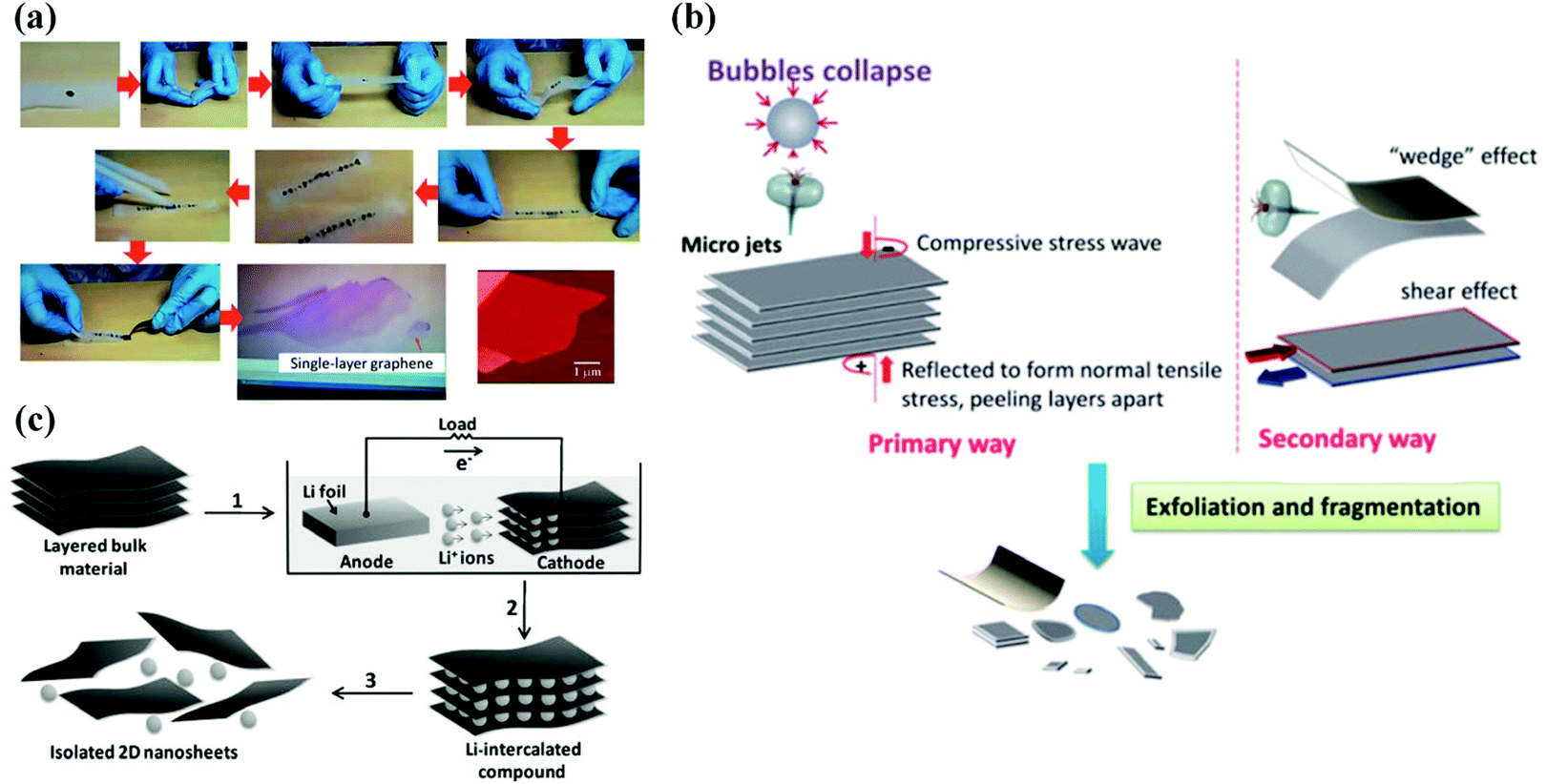 | ||
| Fig. 6 Schematic diagram of top-down methods. (a) Flow chart of mechanical exfoliation method based on scotch tape. Reproduced with permission.97 Copyright 2015, The Royal Society of Chemistry. (b) Illustration of the liquid phase ultrasonic exfoliation method. Reproduced with permission.97 Copyright 2015, The Royal Society of Chemistry. (c) Schematic diagram of the intercalation assisted exfoliation method. Reproduced with permission.98 Copyright 2011, Wiley-VCH. | ||
Liquid phase ultrasonic exfoliation method. Due to the drawbacks of the mechanical exfoliation method that suffers from low yield, one possible solution is to exfoliate the layered compound in the liquid to produce a large number of dispersed nanosheets, which will allow obtaining a large number of 2D materials that can be processed by existing industrial technologies. In the first report of this method, graphene dispersion was obtained by dispersing graphite powder in specific organic solvents, sonication and centrifugation, which opened a whole new outlook for the low-cost and large-scale yield of graphene. One benefit of this method is that it is easy to produce graphene. The biggest disadvantage is that the graphene concentration is extremely low, which is far from practical applications. At present, the exfoliation mechanism of common strategies in the liquid phase originates from liquid cavitation, as shown in Fig. 6(b). In the sonication method, ultrasonic waves generate cavitation bubbles, which collapse into high-energy jets, destroy layered crystallites and produce exfoliated nanosheets. This technology is considered to be very successful in liquid-phase exfoliation of graphene, although it still has several shortcomings of sonication, such as basal and edges planes.
Intercalation assisted exfoliation method. Intercalation assisted exfoliation strategy, where ions or molecules can be inserted between the layers of the multilayer material to reduce the energy barrier of exfoliation, increase the layer spacing and weaken the interlayer adhesion, can achieve a large-scale and high-quality controllable synthesis of materials, which helps to exfoliate the layer with the help of gentle mechanical forces. A schematic description of the intercalation assisted exfoliation method is shown in Fig. 6(c). According to the different intercalants, this strategy can be divided into three categories: molecular intercalation, lithium intercalation and electrochemical intercalation assisted exfoliation.
CVD is a kind of technology that uses plasma excitation, heating and other methods to chemically react reactants under certain temperature and gaseous conditions and deposit the resulting solid substances on the surface of the substrate at an appropriate position to prepare a solid thin film. Using this method can obtain 2D materials100 with very scalable size, controllable thickness, and high quality, making it positive for the application in the electronic industry.
PVD is a thin film preparation technique in which materials are deposited on substrates by means of evaporation, emission and ion beam evaporation in a high vacuum environment. The vacuum coating equipment is a vacuum evaporation coating machine, vacuum magnetron sending coating machine and vacuum ion coating machine. This technique is one of the most efficient methods for preparing thin-film materials in industry and commerce. The reason is that the PVD method can directly prepare 2D materials on the substrate without additional chemical reactions.
4.2 Fabrication methods of 2D multiferroics
At present, the research on 2D multiferroic materials is still on the theoretical prediction, and few of them have been successfully prepared in the experiment. There are mainly several methods for the synthesis for the existing 2D multiferroic materials: CVD, PVD, exfoliation and other strategies.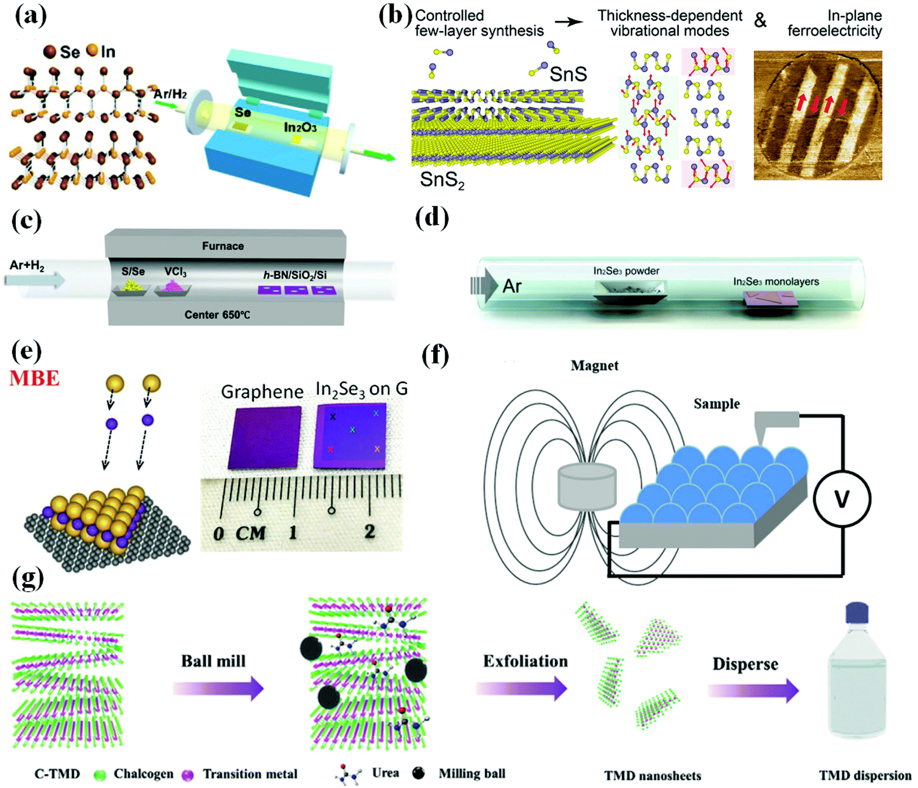 | ||
| Fig. 7 Preparation methods of two-dimensional multiferroic material. (a) Schematic diagram of the growth process of 2D In2Se3 synthesized by the CVD method. Reproduced with permission.101 Copyright 2016, American Chemical Society. (b) Synthesis of few-layer SnS on SnS2 van der Waals substrates. Reproduced with permission.102 Copyright 2021, Elsevier. (c) Illustrations of synthesis of VX2 by CVD strategy. Reproduced with permission.107 Copyright 2018, Wiley-VCH. (d) Process of preparing α-In2Se3 by PVD method. Reproduced with permission.108 Copyright 2015, American Chemical Society. (e) Synthesis of VSe2 monolayers by MBE technology. Reproduced with permission.117 Copyright 2018, Wiley-VCH;110 Copyright 2018, Springer Nature. (f) Schematic drawing of MS setup. Reproduced with permission.118 Copyright 2020, Springer Nature. (g) Schematic illustration of the preparation of MX2 nanosheets by using a solid phase exfoliation strategy. Reproduced with permission.115 Copyright 2020, Wiley-VCH. | ||
108 was prepared by this strategy under atmospheric pressure, and the synthesis process is shown in Fig. 7(d). Recently, Botcha et al.109 fabricated various In2Se3 nanostructures on SiO2/Si substrate using a simple and single-step PVD method, without using metal seed layer on the substrates.
Molecular beam epitaxy growth (MBE) and magnetron sputtering (MS) in PVD are commonly used to prepare 2D multiferroic materials. In 2018, Poh et al.110 used low-temperature MBE technology to synthesize high-quality and large-area monolayer α-In2Se3 on graphene, thereby simplifying the manufacturing of high-performance ferroelectric Schottky diodes for memory applications. The prepared α-In2Se3 film is shown in Fig. 7(e). In addition to the preparation of transition metal dichalcogenide films by CVD technology, experiments have proved that they can also be successfully grown by using the MBE method. Peng111 has obtained a single-layer thickness of TiSe2, demonstrating an alternative method for manufacturing single and few-layer transition metal dichalcogenide materials. In 2005, Posadas et al.112 successfully synthesized epitaxial thin films of multiferroic YMnO3 on GaN/sapphire, which is helpful to study the origin of multiferroicity and the interaction between FE and magnetism in this material. Recently, iodide films (such as CrI3)113 have also been reported to be able to be prepared by MBE technology.
In the process of magnetron sputtering (Fig. 7(f)), a target (or cathode) plate is bombarded by energetic ions generated in a glow discharge plasma situated in front of the target, which is a classic physical deposition process whereby the bombardment process ejects atoms from the target as a result of a collision cascade that subsequently deposits the film. This strategy has been used to prepare perovskite bilayer, such as YMnO thin films,114 and obtained Ca-based double-perovskite bilayer72 have been confirmed to be 2D multiferroic materials with electromagnetic effect.
5. Summary and outlook
In summary, we review the research progress of 2D multiferroic materials and discuss different classifications of 2D multiferroics (Table 1 summarizes some of the reported 2D multiferroic materials). Preparation methods of these materials are also reviewed. Despite many 2D multiferroic materials having been predicted and studied, the exploration of 2D multiferroicity is still in the early stages, especially experimentally. In the process of designing and searching for 2D multiferroic materials, theoretical calculations usually provide directional suggestions for exploring and proving 2D multiferroic properties. Although it is still very challenging to observe stable multiferroicity at room temperature in existing 2D materials, we will have more and more methods to discover new 2D multiferroic materials, including potential physical properties and internal mechanism characterization and manufacturing methods. Since exploring new 2D multiferroic materials has always been an attractive topic, new basic research may address weak electromagnetic coupling effects, depolarization effects, etc. At the same time, the exploration of 2D multiferroicity will also contribute to new scientific frontiers, such as spintronics and valley electronics, which will bring exciting technological advances. Finally, with the discovery of more and more 2D multiferroic materials so far, it is expected that minimization and integration of functional electronics will soon be realized, which will usher in a new scientific era.| Materials | Type | Classification | Date | ||
|---|---|---|---|---|---|
| I/II | Intrinsic/extrinsic | ||||
| 1 | FeTe2O5Br76 | Ferroelectric–ferromagnetic | II | Intrinsic | 2013 |
| 2 | C6N8H organic33 | Ferroelectric–ferromagnetic | I | Intrinsic | 2017 |
| 3 | 2D ferromagnets like MXene, VS2, and MoN211 | Ferroelectric–ferromagnetic | I | Intrinsic | 2017 |
| 4 | Halogen-intercalated phosphorene bilayer93 | Ferroelectric–ferromagnetic | I | Extrinsic | 2017 |
| 5 | 2D CrN and CrB2 systems82 | Ferroelectric–ferromagnetic | I | Intrinsic | 2017 |
| 6 | Monolayer chromium triiodide (CrI3)27 | Ferroelectric–ferromagnetic | I | Extrinsic | 2018 |
| 7 | Double transition metal carbides Hf2MC2T229 |
Ferroelectric–ferromagnetic | II | Intrinsic | 2018 |
| 8 | Transition metal phosphorus chalcogenides28 | Ferroelectric–ferromagnetic | I | Intrinsic | 2018 |
| 9 | CH2OCH3-Functionalized germanene95 | Ferroelectric–ferromagnetic | I | Extrinsic | 2018 |
| 10 | VOCl2 monolayer30 | Ferroelectric–ferromagnetic | I | Intrinsic | 2018 |
| 11 | Transition-metal halide monolayer (CrBr3)2Li91 | Ferroelectric–ferromagnetic | I | Extrinsic | 2018 |
| 12 | NiCl2-Functionalized C2N96 | Ferroelectric–ferromagnetic | I | Extrinsic | 2019 |
| 13 | Ba or Ti deficient BaTiO3 ultrathin film92 | Ferroelectric–ferromagnetic | I | Extrinsic | 2019 |
| 14 | Monolayer CuCrP2S613 | Ferroelectric–ferromagnetic | I | Intrinsic | 2019 |
| 15 | Fe-Doped In2Se3 (Fe0.16In1.84Se3)66 | Ferroelectric–ferromagnetic | I | Intrinsic | 2019 |
| 16 | Monolayer γ-GeSe64 | Ferroelectric–ferromagnetic | I | Intrinsic | 2019 |
| 17 | Mn (Fe)-Doped SnTe monolayer67 | Ferroelectric–ferromagnetic | I | Intrinsic | 2019 |
| 18 | ReWCl6 monolayer83 | Ferroelectric–ferromagnetic | I | Intrinsic | 2020 |
| 19 | 2D ScCrP2Se6 monolayer68 | Ferroelectric–ferromagnetic | I | Intrinsic | 2020 |
| 20 | Li-Decorated α-Fe2O3 (Li@Fe2O3) monolayer94 | Ferroelectric–ferromagnetic | I | Extrinsic | 2020 |
| 21 | BaTiO3 ultrathin film34 | Ferroelectric–ferromagnetic | I | Intrinsic | 2020 |
| 22 | Double-perovskite bilayer with the Fe–Os71 | Ferroelectric–ferromagnetic | I | Intrinsic | 2020 |
| 23 | 2D organometallic framework84 | Ferroelectric–ferromagnetic | I | Intrinsic | 2020 |
| 24 | NiH2SeO4 single crystals85 | Ferroelectric–ferromagnetic | I | Intrinsic | 2020 |
| 25 | VOF2 monolayer74 | Ferroelectric–ferromagnetic | I | Intrinsic | 2020 |
| 26 | 2D van der Waals heterostructures CuInP2S6/InSe69 | Ferroelectric–ferromagnetic | I | Intrinsic | 2020 |
| 27 | 2D bilayer VS278 |
Ferroelectric–ferromagnetic | I | Intrinsic | 2020 |
| 28 | CrN monolayer86 | Ferroelectric–ferromagnetic | I | Intrinsic | 2020 |
| 29 | 2D thin-layer CuCrX2 (X = S or Se)36 | Ferroelectric–ferromagnetic | I | Intrinsic | 2020 |
| 30 | VOI231 |
Ferroelectric–ferromagnetic | I | Intrinsic | 2020 |
| 31 | NiH2SeO485 |
Ferroelectric–ferromagnetic | I | Intrinsic | 2020 |
| 32 | 2D VOCl2 monolayer87 | Ferroelectric–ferromagnetic | I | Intrinsic | 2021 |
| 33 | 2D RMnO3 (R = Tb, Lu and Y)70 | Ferroelectric–ferromagnetic | I | Intrinsic | 2021 |
| 34 | Perovskite bilayer: Ca3Mn2O7 bilayer73 | Ferroelectric–ferromagnetic | I | Intrinsic | 2021 |
| 35 | Ca-Based double-perovskite bilayer72 | Ferroelectric–ferromagnetic | I | Intrinsic | 2021 |
| 36 | Hole-doped and arsenic-doped monolayer α-In2Se365 |
Ferroelectric–ferromagnetic | I | Intrinsic | 2021 |
| 37 | CrNCl2 monolayer77 | Ferroelectric–ferromagnetic | I | Intrinsic | 2021 |
| 38 | VOF monolayer75 | Ferroelectric–ferromagnetic | I | Intrinsic | 2021 |
| 39 | SnS, SnSe, GeS, and GeSe monolayers12,39 | Ferroelectric–ferroelastic | N/A | Intrinsic | 2016 |
| 40 | Group IV monochalcogenides40 | Ferroelectric–ferroelastic | N/A | Intrinsic | 2017 |
| 41 | Bi2O2Se, Bi2O2S and Bi2O2Te41 | Ferroelectric–ferroelastic | N/A | Intrinsic | 2017 |
| 42 | Boron pentaphosphide (BP5) monolayer14 | Ferroelectric–ferroelastic | N/A | Intrinsic | 2017 |
| 43 | GaTeCl monolayer79 | Ferroelectric–ferroelastic | N/A | Intrinsic | 2018 |
| 44 | Silver and copper monohalides42 | Ferroelectric–ferroelastic | N/A | Intrinsic | 2019 |
| 45 | Nb2SiTe4 and Nb2GeTe488 |
Ferroelectric–ferroelastic | N/A | Intrinsic | 2019 |
| 46 | β-GeSe and α-SnTe monolayer119 | Ferroelectric–ferroelastic | N/A | Intrinsic | 2021 |
| 47 | Bilayer ZrI243 |
Ferroelectric–ferroelastic | N/A | Intrinsic | 2021 |
| 48 | α-SnO45 | Ferromagnetic–ferroelastic | N/A | Intrinsic | 2016 |
| 49 | H type Janus-VSSe81 | Ferromagnetic–ferroelastic | N/A | Intrinsic | 2018 |
| 50 | CrSX (X = Cl, Br, I) monolayers35 | Ferromagnetic–ferroelastic | N/A | Intrinsic | 2020 |
| 51 | Monolayer α-PbO120 | Ferromagnetic–ferroelastic | N/A | Extrinsic | 2020 |
| 52 | Tetragonal structures XOBr (X = Tc, Ru)47 | Ferromagnetic–ferroelastic | N/A | Intrinsic | 2020 |
| 53 | Vanadium tetrafluoride (VF4) monolayer80 | Ferromagnetic–ferroelastic | N/A | Intrinsic | 2020 |
| 54 | Single-layer AgF244 |
Ferromagnetic–ferroelastic | N/A | Intrinsic | 2020 |
| 55 | Li-Doped GdI3 monolayer63 | Ferromagnetic–ferroelastic | N/A | Intrinsic | 2021 |
| 56 | Transition-metal-doped group-IVmonochalcogenides62 | Ferroelectric–ferromagnetic–ferroelastic | N/A | Intrinsic | 2018 |
| 57 | FeOOH monolayer89 | Ferroelectric–ferromagnetic–ferroelastic | N/A | Intrinsic | 2020 |
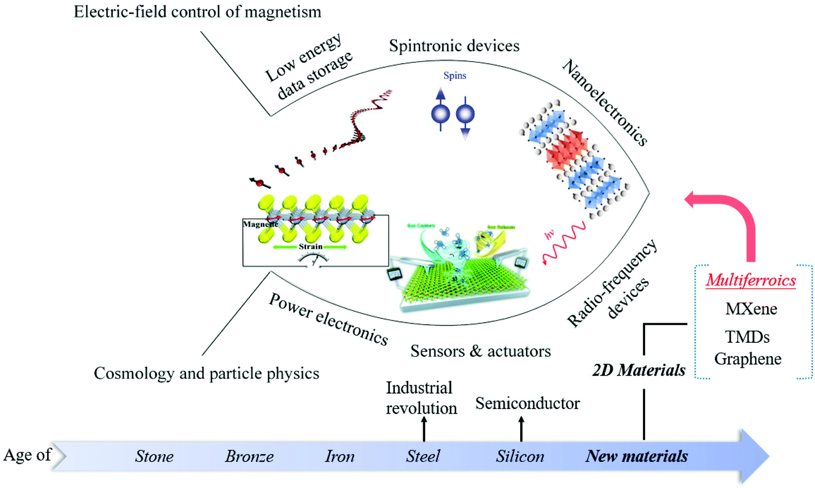
Since the beginning of the 21st century, the research and development of new materials have become fierce, especially the exploration of micro and nanomaterials is changing with each passing day. As a large family of new materials, 2D materials are favoured by academia because of their unique physical properties. From the birth of graphene in 2004 to the synthesis of MXene in 2011, the research and application of a new generation of 2D materials have sprung up. However, the research on 2D multiferroic materials has just begun.
The ability of multiferroics to regulate magnetism using electric fields via their magnetoelectric coupling has been the major technical push for their exploration. Because the generation of electric fields uses considerably less energy than the production of magnetic fields utilized in most present magnetism-based devices, such a capacity might be technologically revolutionary. Multiferroicity has been utilized to tackle fundamental cosmological and particle physics difficulties. The fact that any electric dipole moment with symmetry requirements takes the same axis as its magnetic dipole moment has been utilized to discover the electric dipole moment of the electron, which is ideally multiferroic. When the ferroelectric polarization is switched in the applied electric field, the developed multiferroic material (Eu, Ba)TiO3 is utilized to monitor the change in the net magnetic moment, allowing the upper limit of the achievable value of the electronic electric dipole moment to be retrieved. This number is significant because it indicates the amount of time-reversal symmetry breaches in the cosmos, which places severe constraints on the theory of basic particle physics.
2D multiferroic materials have a wide range of application prospects in the following fields (Fig. 8). 1. Low energy data storage:121 unlike traditional storage devices that use electricity to calculate and magnets to store data, memories based on 2D multiferroic materials use electricity to calculate and store data simultaneously. 2. Spintronics:122 spintronic devices based on 2D ferromagnetic materials are promising as spintronic devices rely on nanomaterials with a size smaller than the spin relaxation length and adjustable interface characteristics. However, the disordered system obtained by the traditional method usually has low magnetic properties and is not suitable for the application. Therefore, searching for 2D materials with inherent magnetic properties is the ultimate goal of spintronics for 2D materials. 3. Nanoelectronics:123 electronic devices based on 2D multiferroic materials can make the devices have higher rectification characteristics and easier to realize the manufacture of PN junctions, thereby providing a way for nano-devices with diverse functions. However, the preparation and growth mechanism of 2D multiferroic materials is still in the exploratory stage, which limits the development of 2D multiferroic equipment. 4. Power electronics:81 2D multiferroic materials with piezoelectric effect have become the main focus of energy harvesting application research, ranging from small-scale low-power electronic devices to large-scale industrial applications, such as self-powered sensor devices,124 environmental monitoring, and large-scale power generation. 5. Sensor & actuator:125 2D multiferroic with piezoelectric effect are also ideal materials for sensors and actuators with wearable and low power consumption. 6. Microwave and Radio Frequency (RF) devices: the multiferroic heterojunction with both ferroelectric and ferromagnetic properties can achieve voltage-controlled magnetic properties through the strain-induced magnetoelectric coupling effect. Therefore, the microwave and RF device prepared by this mechanism can meet the requirements of miniaturization, ultra-fast response and low power consumption, and can realize new functionality. The development of such devices provides broad prospects for the realization of next-generation tunable magnetic microwave components, ultra-low power electronic devices and spintronic components.
 | ||
| Fig. 8 Prospects of 2D multiferroic materials. Illustration of the low energy data storage, Reproduced with permission,121 Copyright 2020, Wiley-VCH. Illustration of nanoelectronics, Reproduced with permission,123 Copyright 2019, Springer Nature. Illustration of sensors & actuators. Reproduced with permission,125 Copyright 2020, The Royal Society of Chemistry. Illustration of power electronics, Reproduced with permission.81 Copyright 2019, The Royal Society of Chemistry. | ||
Conflicts of interest
There are no conflicts to declare.Acknowledgements
Dr Mingyuan Gao acknowledges the support from National Natural Science Foundation of China (Grant No. 52008343) and Natural Science Foundation of Chongqing, China (Grant No. cstc2021jcyj-msxmX1128). The authors acknowledge funding support from ANU PhD student scholarship, Australian Research Council (ARC; No. DP180103238), and Australian National Heart Foundation (ARIES ID: 35852). Dr Yunye Gao acknowledges the sponsorship under the China Scholarship Council (CSC) funding project.References
- K. Zhai, D.-S. Shang, Y.-S. Chai, G. Li, J.-W. Cai, B.-G. Shen and Y. Sun, Adv. Funct. Mater., 2018, 28, 1705771 CrossRef.
- M. Bichurin, R. Petrov, V. Leontiev, G. Semenov and O. Sokolov, Sensors, 2017, 17, 1271 CrossRef PubMed.
- Z. Yang, S. Zhou, J. Zu and D. Inman, Joule, 2018, 2, 642–697 CrossRef CAS.
- N. Hiremath, R. Guntupalli, V. Vodyanoy, B. A. Chin and M.-K. Park, Sens. Actuators, B, 2015, 210, 129–136 CrossRef CAS.
- J. Zhang, B. Wang, M. Tebyetekerwa, Y. Zhu, B. Liu, H. T. Nguyen, S. Tian, Y. Zhang and Y. Lu, J. Mater. Chem. C, 2019, 7, 15074–15081 RSC.
- M. Gao, P. Wang, L. Jiang, B. Wang, Y. Yao, S. Liu, D. Chu, W. Cheng and Y. Lu, Energy Environ. Sci., 2021, 14, 2114–2157 RSC.
- Y. Zhu, Z. Li, L. Zhang, B. Wang, Z. Luo, J. Long, J. Yang, L. Fu and Y. Lu, ACS Appl. Mater. Interfaces, 2018, 10, 43291–43298 CrossRef CAS.
- Z. Lu, G. P. Neupane, G. Jia, H. Zhao, D. Qi, Y. Du, Y. Lu and Z. Yin, Adv. Funct. Mater., 2020, 30, 2001127 CrossRef CAS.
- J. Pei, J. Yang, T. Yildirim, H. Zhang and Y. Lu, Adv. Mater., 2019, 31, e1706945 CrossRef PubMed.
- K. S. Novoselov, A. K. Geim, S. V. Morozov, D. Jiang, Y. Zhang, S. V. Dubonos, I. V. Grigorieva and A. A. Firsov, Science, 2004, 306, 666–669 CrossRef CAS PubMed.
- L. Li and M. Wu, ACS Nano, 2017, 11, 6382–6388 CrossRef CAS PubMed.
- M. Wu and X. C. Zeng, Nano Lett., 2016, 16, 3236–3241 CrossRef CAS.
- Y. Lai, Z. Song, Y. Wan, M. Xue, C. Wang, Y. Ye, L. Dai, Z. Zhang, W. Yang, H. Du and J. Yang, Nanoscale, 2019, 11, 5163–5170 RSC.
- H. Wang, X. Li, J. Sun, Z. Liu and J. Yang, 2D Mater., 2017, 4, 045020 CrossRef.
- K. Cho, J. Yang and Y. Lu, J. Mater. Res., 2017, 32, 2839–2847 CrossRef CAS.
- E. Blundo, C. Di Giorgio, G. Pettinari, T. Yildirim, M. Felici, Y. Lu, F. Bobba and A. Polimeni, Adv. Mater. Interfaces, 2020, 7, 2000621 CrossRef CAS.
- C. Di Giorgio, E. Blundo, G. Pettinari, M. Felici, Y. Lu, A. M. Cucolo, A. Polimeni and F. Bobba, Adv. Mater. Interfaces, 2020, 7, 2001024 CrossRef CAS.
- D. Tedeschi, E. Blundo, M. Felici, G. Pettinari, B. Liu, T. Yildrim, E. Petroni, C. Zhang, Y. Zhu, S. Sennato, Y. Lu and A. Polimeni, Adv. Mater., 2019, 31, e1903795 CrossRef PubMed.
- A. R. Khan, T. Lu, W. Ma, Y. Lu and Y. Liu, Adv. Electron. Mater., 2020, 6, 1901381 CrossRef CAS.
- S. Rahman, B. Liu, B. Wang, Y. Tang and Y. Lu, ACS Appl. Mater. Interfaces, 2021, 13, 7423–7433 CrossRef CAS PubMed.
- B. Wen, Y. Zhu, D. Yudistira, A. Boes, L. Zhang, T. Yidirim, B. Liu, H. Yan, X. Sun, Y. Zhou, Y. Xue, Y. Zhang, A. Mitchell, H. Zhang and Y. Lu, ACS Nano, 2019, 13, 5335–5343 CrossRef CAS PubMed.
- L. Zhang, H. Yan, X. Sun, M. Dong, T. Yildirim, B. Wang, B. Wen, G. P. Neupane, A. Sharma, Y. Zhu, J. Zhang, K. Liang, B. Liu, H. T. Nguyen, D. Macdonald and Y. Lu, Nanoscale, 2019, 11, 418–425 RSC.
- M. Tebyetekerwa, J. Zhang, K. Liang, T. Duong, G. P. Neupane, L. Zhang, B. Liu, T. N. Truong, R. Basnet, X. Qiao, Z. Yin, Y. Lu, D. Macdonald and H. T. Nguyen, Adv. Mater., 2019, 31, e1900522 CrossRef.
- M. An and S. Dong, APL Mater., 2020, 8, 110704 CrossRef CAS.
- L. W. Martin, S. P. Crane, Y. H. Chu, M. B. Holcomb, M. Gajek, M. Huijben, C. H. Yang, N. Balke and R. Ramesh, J. Phys.: Condens. Matter, 2008, 20, 434220 CrossRef.
- E. Ascher, H. Rieder, H. Schmid and H. Stössel, J. Appl. Phys., 1966, 37, 1404–1405 CrossRef CAS.
- Y. Zhao, L. Lin, Q. Zhou, Y. Li, S. Yuan, Q. Chen, S. Dong and J. Wang, Nano Lett., 2018, 18, 2943–2949 CrossRef CAS PubMed.
- W. Wan, C. Liu, W. Xiao and Y. Yao, Appl. Phys. Lett., 2017, 111, 132904 CrossRef.
- J. J. Zhang, L. Lin, Y. Zhang, M. Wu, B. I. Yakobson and S. Dong, J. Am. Chem. Soc., 2018, 140, 9768–9773 CrossRef CAS PubMed.
- H. Ai, X. Song, S. Qi, W. Li and M. Zhao, Nanoscale, 2019, 11, 1103–1110 RSC.
- N. Ding, J. Chen, S. Dong and A. Stroppa, Phys. Rev. B, 2020, 102, 165129 CrossRef CAS.
- C. Xu, P. Chen, H. Tan, Y. Yang, H. Xiang and L. Bellaiche, Phys. Rev. Lett., 2020, 125, 037203 CrossRef CAS PubMed.
- Z. Tu, M. Wu and X. C. Zeng, J. Phys. Chem. Lett., 2017, 8, 1973–1978 CrossRef CAS PubMed.
- H. Gao, T. Lin, Y. Yan, K. Fu, Y. Liu and X. Liu, Phys. Chem. Chem. Phys., 2020, 22, 18284–18293 RSC.
- J. Qi, H. Wang, X. Chen and X. Qian, Appl. Phys. Lett., 2018, 113, 043102 CrossRef.
- T. Zhong, X. Li, M. Wu and J.-M. Liu, Natl. Sci. Rev., 2020, 7, 373–380 CrossRef CAS PubMed.
- A. R. Khan, B. Liu, L. Zhang, Y. Zhu, X. He, L. Zhang, T. Lü and Y. Lu, Adv. Opt. Mater., 2020, 8, 2000441 CrossRef CAS.
- A. R. Khan, B. Liu, T. Lü, L. Zhang, A. Sharma, Y. Zhu, W. Ma and Y. Lu, ACS Nano, 2020, 14, 15806–15815 CrossRef PubMed.
- H. Wang and X. Qian, 2D Mater., 2017, 4, 015042 CrossRef.
- H. Wang and X. Qian, Nano Lett., 2017, 17, 5027–5034 CrossRef CAS PubMed.
- M. Wu and X. C. Zeng, Nano Lett., 2017, 17, 6309–6314 CrossRef CAS PubMed.
- Y. Gao, M. Wu and X. C. Zeng, Nanoscale Horiz., 2019, 4, 1106–1112 RSC.
- T. Zhang, Y. Liang, X. Xu, B. Huang, Y. Dai and Y. Ma, Phys. Rev. B, 2021, 103, 165420 CrossRef CAS.
- X. Xu, Y. Ma, T. Zhang, C. Lei, B. Huang and Y. Dai, Nanoscale Horiz., 2020, 5, 1386–1393 RSC.
- L. Seixas, A. S. Rodin, A. Carvalho and A. H. Castro Neto, Phys. Rev. Lett., 2016, 116, 206803 CrossRef CAS PubMed.
- B. Xu, S. Li, K. Jiang, J. Yin, Z. Liu, Y. Cheng and W. Zhong, Appl. Phys. Lett., 2020, 116, 052403 CrossRef CAS.
- Z.-x. Pang, W.-x. Ji, C.-w. Zhang, P.-j. Wang and P. Li, Chem. Phys. Lett., 2021, 763, 138163 CrossRef CAS.
- D. Khomskii, Physics, 2009, 2 DOI:10.1103/Physics.2.20.
- S. Dong, J.-M. Liu, S.-W. Cheong and Z. Ren, Adv. Phys., 2015, 64, 519–626 CrossRef CAS.
- Y. Bai, H. Zhao, J. Chen, Y. Sun and S. Zhao, Ceram. Int., 2016, 42, 10304–10309 CrossRef CAS.
- P. R. Mickel, H. Jeen, P. Kumar, A. Biswas and A. F. Hebard, Phys. Rev. B, 2016, 93, 134205 CrossRef.
- L. H. d. S. Lacerda and S. R. de Lazaro, J. Magn. Magn. Mater., 2020, 500, 166364 CrossRef CAS.
- F. Y. Nad, P. Monceau, C. Carcel and J. M. Fabre, Synth. Met., 2003, 133–134, 265–267 CrossRef CAS.
- N. Ikeda, H. Ohsumi, K. Ohwada, K. Ishii, T. Inami, K. Kakurai, Y. Murakami, K. Yoshii, S. Mori, Y. Horibe and H. Kito, Nature, 2005, 436, 1136–1138 CrossRef CAS PubMed.
- P. Jarillo-Herrero, S. Sapmaz, C. Dekker, L. P. Kouwenhoven and H. S. Van Der Zant, Nature, 2004, 429, 389–392 CrossRef CAS.
- Y. J. Choi, H. T. Yi, S. Lee, Q. Huang, V. Kiryukhin and S. W. Cheong, Phys. Rev. Lett., 2008, 100, 047601 CrossRef CAS PubMed.
- B. B. Van Aken, T. T. Palstra, A. Filippetti and N. A. Spaldin, Nat. Mater., 2004, 3, 164–170 CrossRef CAS PubMed.
- N. M. Avram, M. G. Brik and E. L. Andreici, Phys. Scr., 2014, T162, 014020 CrossRef CAS.
- M. Fiebig, T. Lottermoser, D. Meier and M. Trassin, Nat. Rev. Mater., 2016, 1, 16046 CrossRef CAS.
- S. M. Yakout, J. Supercond. Novel Magn., 2021, 34, 317–338 CrossRef CAS.
- Y. Tokura, S. Seki and N. Nagaosa, Rep. Prog. Phys., 2014, 77, 076501 CrossRef PubMed.
- L. Yang, M. Wu and K. Yao, Nanotechnology, 2018, 29, 215703 CrossRef PubMed.
- H. You, Y. Zhang, J. Chen, N. Ding, M. An, L. Miao and S. Dong, Phys. Rev. B, 2021, 103, L161408 CrossRef CAS.
- C. Liu, S. Guan, H. Yin, W. Wan, Y. Wang and Y. Zhang, Appl. Phys. Lett., 2019, 115, 252904 CrossRef.
- X. Duan, J. Huang, B. Xu and S. Liu, Mater. Horiz., 2021, 8, 2316–2324 RSC.
- H. Yang, L. Pan, M. Xiao, J. Fang, Y. Cui and Z. Wei, Sci. China Mater., 2020, 63, 421–428 CrossRef CAS.
- Y. Liu, W. Zhou, G. Tang, C. Yang, X. Wang and J. Hong, J. Phys. Chem. C, 2019, 123, 28919–28924 CrossRef.
- X. Feng, J. Liu, X. Ma and M. Zhao, Phys. Chem. Chem. Phys., 2020, 22, 7489–7496 RSC.
- Z. Zhu, X. Chen, W. Li and J. Qi, J. Mater. Chem. C, 2020, 8, 17342–17348 RSC.
- G. E. Tongue Magne, R. M. Keumo Tsiaze, A. J. Fotué, N. M. Hounkonnou and L. C. Fai, Phys. Lett. A, 2021, 400, 127305 CrossRef CAS.
- J. Zhang, X. Shen, Y. Wang, C. Ji, Y. Zhou, J. Wang, F. Huang and X. Lu, Phys. Rev. Lett., 2020, 125, 017601 CrossRef CAS PubMed.
- X. Shen, Q. Luo, Z. Wu, Y. Zhou, J. Wang, J. Zhang, J. Su and X. Lu, Phys. Rev. B, 2021, 103, L220406 CrossRef CAS.
- Y. Zhou, Z. Chen, Z. Wu, X. Shen, J. Wang, J. Zhang and H. Sun, Phys. Rev. B, 2021, 103, 224409 CrossRef CAS.
- H. P. You, N. Ding, J. Chen and S. Dong, Phys. Chem. Chem. Phys., 2020, 22, 24109–24115 RSC.
- S. Xu, F. Jia, G. Zhao, W. Wu and W. Ren, J. Mater. Chem. C, 2021, 9, 9130–9136 RSC.
- J. Chakraborty, N. Ganguli, T. Saha-Dasgupta and I. Dasgupta, Phys. Rev. B: Condens. Matter Mater. Phys., 2013, 88, 094409 CrossRef.
- W. Shen, Y. Pan, S. Shen, H. Li, S. Nie and J. Mei, Chin. Phys. B, 2021 DOI:10.1088/1674-1056/ac0787.
- X. Liu, A. P. Pyatakov and W. Ren, Phys. Rev. Lett., 2020, 125, 247601 CrossRef CAS PubMed.
- S. H. Zhang and B. G. Liu, Nanoscale, 2018, 10, 5990–5996 RSC.
- L. Zhang, C. Tang and A. Du, J. Mater. Chem. C, 2021, 9, 95–100 RSC.
- J. Yang, A. Wang, S. Zhang, J. Liu, Z. Zhong and L. Chen, Phys. Chem. Chem. Phys., 2018, 21, 132–136 RSC.
- W. Luo, K. Xu and H. Xiang, Phys. Rev. B, 2017, 96, 235415 CrossRef.
- M. Xu, C. Huang, Y. Li, S. Liu, X. Zhong, P. Jena, E. Kan and Y. Wang, Phys. Rev. Lett., 2020, 124, 067602 CrossRef CAS PubMed.
- X. Li, X. Li and J. Yang, J. Phys. Chem. Lett., 2020, 11, 4193–4197 CrossRef CAS PubMed.
- B. Yu, Y. Shen, S. Yang, D. Xu, J. Lin, L. Sun, B. Tian, Q. Zhu, C. Duan and Q. Zhao, J. Mater. Chem. C, 2020, 8, 14812–14818 RSC.
- J. Liang, Q. Cui and H. Yang, Phys. Rev. B, 2020, 102, 220409(R) CrossRef.
- A. Mahajan and S. Bhowmick, Phys. Rev. B, 2021, 103, 075436 CrossRef CAS.
- T. Zhang, Y. Ma, X. Xu, C. Lei, B. Huang and Y. Dai, J. Phys. Chem. Lett., 2020, 11, 497–503 CrossRef CAS PubMed.
- X. Feng, X. Ma, L. Sun, J. Liu and M. Zhao, J. Mater. Chem. C, 2020, 8, 13982–13989 RSC.
- Y. Zhou, D. Wu, Y. Zhu, Y. Cho, Q. He, X. Yang, K. Herrera, Z. Chu, Y. Han, M. C. Downer, H. Peng and K. Lai, Nano Lett., 2017, 17, 5508–5513 CrossRef CAS PubMed.
- C. Huang, Y. Du, H. Wu, H. Xiang, K. Deng and E. Kan, Phys. Rev. Lett., 2018, 120, 147601 CrossRef PubMed.
- H. Gao, Z. Yue, Y. Liu, J. Hu and X. Li, Nanomaterials, 2019, 9, 269 CrossRef CAS PubMed.
- Q. Yang, W. Xiong, L. Zhu, G. Gao and M. Wu, J. Am. Chem. Soc., 2017, 139, 11506–11512 CrossRef CAS PubMed.
- J. Shang, C. Li, X. Tang, A. Du, T. Liao, Y. Gu, Y. Ma, L. Kou and C. Chen, Nanoscale, 2020, 12, 14847–14852 RSC.
- L. Kou, Y. Ma, T. Liao, A. Du and C. Chen, Phys. Rev. Appl., 2018, 10, 024043 CrossRef CAS.
- L. Li, M. Wu and X. C. Zeng, Adv. Funct. Mater., 2019, 29, 1905752 CrossRef CAS.
- M. Yi and Z. Shen, J. Mater. Chem. A, 2015, 3, 11700–11715 RSC.
- Z. Zeng, Z. Yin, X. Huang, H. Li, Q. He, G. Lu, F. Boey and H. Zhang, Angew. Chem., Int. Ed., 2011, 50, 11093–11097 CrossRef CAS PubMed.
- L. Zhang, M. Mehedi Hasan, Y. Tang, A. Raza Khan, H. Yan, T. Yildirim, X. Sun, J. Zhang, J. Zhu, Y. Zhang and Y. Lu, Mater. Today, 2021 DOI:10.1016/j.mattod.2021.02.021.
- J. Zhang, Y. Zhu, M. Tebyetekerwa, D. Li, D. Liu, W. Lei, L. Wang, Y. Zhang and Y. Lu, ACS Appl. Nano Mater., 2020, 4, 769–777 CrossRef.
- W. Feng, W. Zheng, F. Gao, X. Chen, G. Liu, T. Hasan, W. Cao and P. Hu, Chem. Mater., 2016, 28, 4278–4283 CrossRef CAS.
- P. Sutter, H. P. Komsa, H. Lu, A. Gruverman and E. Sutter, Nano Today, 2021, 37, 101082 CrossRef CAS.
- H. Wang, Y. Chen, M. Duchamp, Q. Zeng, X. Wang, S. H. Tsang, H. Li, L. Jing, T. Yu, E. H. T. Teo and Z. Liu, Adv. Mater., 2018, 30, 1704382 CrossRef PubMed.
- W. Fu, Y. Chen, J. Lin, X. Wang, Q. Zeng, J. Zhou, L. Zheng, H. Wang, Y. He, H. He, Q. Fu, K. Suenaga, T. Yu and Z. Liu, Chem. Mater., 2016, 28, 7613–7618 CrossRef CAS.
- H. Wang, X. Huang, J. Lin, J. Cui, Y. Chen, C. Zhu, F. Liu, Q. Zeng, J. Zhou, P. Yu, X. Wang, H. He, S. H. Tsang, W. Gao, K. Suenaga, F. Ma, C. Yang, L. Lu, T. Yu, E. H. T. Teo, G. Liu and Z. Liu, Nat. Commun., 2017, 8, 394 CrossRef PubMed.
- X. Wang, J. Lin, Y. Zhu, C. Luo, K. Suenaga, C. Cai and L. Xie, Nanoscale, 2017, 9, 16607–16611 RSC.
- M. Hossain, J. Wu, W. Wen, H. Liu, X. Wang and L. Xie, Adv. Mater. Interfaces, 2018, 5, 800528 Search PubMed.
- J. Zhou, Q. Zeng, D. Lv, L. Sun, L. Niu, W. Fu, F. Liu, Z. Shen, C. Jin and Z. Liu, Nano Lett., 2015, 15, 6400–6405 CrossRef CAS PubMed.
- V. D. Botcha, Y. Hong, Z. Huang, Z. Li, Q. Liu, J. Wu, Y. Lu and X. Liu, J. Alloys Compd., 2019, 773, 698–705 CrossRef CAS.
- S. M. Poh, S. J. R. Tan, H. Wang, P. Song, I. H. Abidi, X. Zhao, J. Dan, J. Chen, Z. Luo, S. J. Pennycook, A. H. Castro Neto and K. P. Loh, Nano Lett., 2018, 18, 6340–6346 CrossRef CAS.
- J.-P. Peng, J.-Q. Guan, H.-M. Zhang, C.-L. Song, L. Wang, K. He, Q.-K. Xue and X.-C. Ma, Phys. Rev. B: Condens. Matter Mater. Phys., 2015, 91, 21113 CrossRef.
- A. Posadas, J. B. Yau, C. H. Ahn, J. Han, S. Gariglio, K. Johnston, K. M. Rabe and J. B. Neaton, Appl. Phys. Lett., 2005, 87, 171915 CrossRef.
- X. Cai, Z. Xu, S.-H. Ji, N. Li and X. Chen, Chin. Phys. B, 2021, 30, 028102 CrossRef CAS.
- D. C. Yoo, J. Y. Lee, I. S. Kim and Y. T. Kim, Thin Solid Films, 2002, 416, 62–65 CrossRef CAS.
- L. Zhang, C. Chen, J. Zhou, G. Yang, J. Wang, D. Liu, Z. Chen and W. Lei, Adv. Funct. Mater., 2020, 30, 2004139 CrossRef CAS.
- K.-T. Kim and C.-I. Kim, J. Eur. Ceram. Soc., 2004, 24, 2613–2617 CrossRef CAS.
- X. Wang, Z. Song, W. Wen, H. Liu, J. Wu, C. Dang, M. Hossain, M. A. Iqbal and L. Xie, Adv. Mater., 2019, 31, e1804682 CrossRef PubMed.
- S. Meenachisundaram, N. Wakiya, C. Muthamizhchelvan, P. Gangopadhyay, N. Sakamoto and S. Ponnusamy, J. Electron. Mater., 2021, 50, 1699–1706 CrossRef CAS.
- J. Zhou and S. Zhang, npj 2D Mater. Appl., 2021, 5, 16 CrossRef CAS.
- M.-H. Zhang, X.-L. Chen, W.-X. Ji, P.-J. Wang, Y. Min and C.-W. Zhang, Appl. Phys. Lett., 2020, 116, 172105 CrossRef.
- S. R. Burns, O. Paull, J. Juraszek, V. Nagarajan and D. Sando, Adv. Mater., 2020, 32, 2003711 CrossRef CAS PubMed.
- A. Hirohata and K. Takanashi, J. Phys. D: Appl. Phys., 2014, 47, 193001 CrossRef.
- N. A. Spaldin and R. Ramesh, Nat. Mater., 2019, 18, 203–212 CrossRef CAS PubMed.
- Y. Sun, P. Wang, J. Lu, J. Xu, P. Wang, S. Xie, Y. Li, J. Dai, B. Wang and M. Gao, Appl. Energy, 2021, 286, 116512 CrossRef.
- A. Hirohata, K. Yamada, Y. Nakatani, I.-L. Prejbeanu, B. Diény, P. Pirro and B. Hillebrands, J. Magn. Magn. Mater., 2020, 509, 166711 CrossRef CAS.
| This journal is © The Royal Society of Chemistry 2021 |