DOI:
10.1039/D0TA08190F
(Review Article)
J. Mater. Chem. A, 2020,
8, 24943-24976
Recent advances in 2D/nanostructured metal sulfide-based gas sensors: mechanisms, applications, and perspectives
Received
20th August 2020
, Accepted 23rd October 2020
First published on 30th October 2020
Abstract
2D and nanostructured metal sulfide materials are promising in the advancement of several gas sensing applications due to the abundant choice of materials with easily tunable electronic, optical, physical, and chemical properties. These applications are particularly attractive for gas sensing in environmental monitoring and breath analysis. This review gives a systematic description of various gas sensors based on 2D and nanostructured metal sulfide materials. Firstly, the crystal structures of metal sulfides are introduced. Secondly, the gas sensing mechanisms of different metal sulfides based on density functional theory analysis are summarised. Various gas-sensing concepts of metal sulfide-based devices, including chemiresistors, functionalized metal sulfides, Schottky junctions, heterojunctions, field-effect transistors, and optical and surface acoustic wave sensors, are compared and presented. It then discusses the extensive applications of metal sulfide-based sensors for different gas molecules, including volatile organic compounds (i.e., acetone, benzene, methane, formaldehyde, ethanol, and liquefied petroleum gas) and inorganic gas (i.e., CO2, O2, NH3, H2S, SO2, NOx, CH4, H2, and humidity). Finally, a strengths–weaknesses–opportunities–threats (SWOT) analysis is proposed for future development and commercialization in this field.
1. Introduction
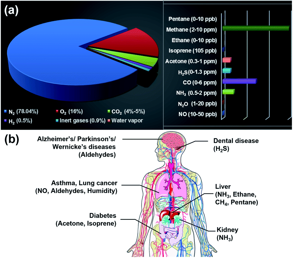
Nanostructured materials have been considered promising candidates for gas sensing applications due to their large surface area, abundant surface-active sites, and high surface reactivity.1 They are primarily used for monitoring air quality, the environmental situation, and breath. Typically, atmospheric pollutants include nitrogen dioxide (NO2), nitrogen monoxide (NO), ammonia (NH3), hydrogen sulfide (H2S), sulfur dioxide (SO2), carbon monoxide (CO), carbon dioxide (CO2), methane (CH4), and volatile organic compounds (VOCs).2 When these pollutants exceed the recommended exposure limits, they have negative effects on the environment and human health (Table 1). Therefore, the gas sensor needs to detect different gases simultaneously with high sensitivity and selectivity, a small size, low cost, and low power consumption (<10 mW).3 In the aspect of breath analysis, different biomarkers from exhaled breath need to be recognized accurately.4 Normally, human breath contains nitrogen (N2), oxygen (O2), CO2, hydrogen (H2), inert gases, and water vapour. Sometimes, it includes organic VOCs viz. acetone, ethanol, isoprene, ethane, methane, pentane, etc., and inorganic gases such as NOx, NH3, COx, and H2S, see Fig. 1a. These excretory products diffuse into the inhaled air in the alveoli of the lungs and are then ejected in the form of exhaled air. Therefore, exhaled air carries different biomarkers, which can be used as fingerprints of metabolic products. This enables early diagnosis and prevention of respiratory diseases such as lung cancer, diseases of the kidneys, prostate, and bladder, and even Parkinson's disease, see Fig. 1b.5,6 However, the maximum permissible limits of biomarkers are mostly at the parts-per-billion (ppb) level, which requires a highly sensitive gas sensor with a low limit of detection (LOD).
Table 1 The environmental and human health impacts of different air pollutants and their maximum permissible limits set by the European Union7,8
| Gas |
Environmental and human health impact |
Maximum permissible limit |
Value of interest (ppb) |
| 8 hours (ppm) |
Short-term (15 min, ppm) |
| NO2 |
Indirect green house gas, acidification, eutrophication, cardiovascular mortality, asthma, lung function |
0.5 |
1 |
21 |
| NH3 |
Toxic, PM2.5 precursor |
20 |
50 |
20![[thin space (1/6-em)]](https://www.rsc.org/images/entities/char_2009.gif) 000 000 |
| H2S |
SO2 precursor, toxic |
5 |
10 |
5000 |
| SO2 |
Indirect green house gas, acidification, particulate matter, precursor, cardiovascular mortality |
0.5 |
1 |
7.5 |
| CO |
Indirect green house gas, toxic, asthma, cardiovascular disease, cardiac disease, psychiatric admissions, etc. |
20 |
100 |
4000 |
| CO2 |
Green house gas – climate change |
5000 |
— |
400000 |
| CH4 |
Green house gas – climate change |
1000 |
— |
1800 |
 |
| | Fig. 1 (a) The gas contents of human breath and (b) the biomarkers of different diseases. | |
Solid-state sensors such as metal oxide semiconductors (MOSs),9 carbon-based nanomaterials (CNMs),10–12 and metal sulfide semiconductors13 are used extensively in gas detection research. After Taguchi patented the first oxide-based gas sensor in 1962, various high sensitivity and low-cost gas sensors based on MOSs have been developed.14 Tungsten oxide (WO3) nanotubes have been proved as a potential MOS for the detection of NO at the ppb level.15 Orthorhombic molybdenum trioxide (α-MoO3) nanoribbons can detect NH3 down to 280 ppt.16 Gas sensors based on Pt functionalized tin dioxide (SnO2)17 or indium oxide (In2O3)18 can detect the lowest acetone concentration of 10 ppb. The ZnSnO3 gas sensor can detect 100 ppb ethanol.19 Many MOS-based devices can detect H2S at less than 1 ppm, such as copper oxide (CuO), SnO2, In2O3, zinc oxide (ZnO), titanium oxide (TiO2), and iron oxide (Fe2O3).20 However, the operating temperature (OT) of MOS-based devices is usually high (100–300 °C), which induces high power consumption and consequently hinders the gas-sensing applications. CNMs, such as graphene and its derivatives and carbon nanotubes (CNTs), were employed as chemical gas sensors owing to their outstanding characteristics of a mesoporous nature, a large specific surface area, and enhanced electron transport properties.21 Pristine reduced graphene oxide (rGO) can detect NH3 and NOx, and rGO with a functionally modified surface (such as rGO/ZnO, rGO/Pt, and rGO/Ni) are known to detect VOCs (such as acetone, phenol, and nitrobenzene).22–24 Rigoni et al.25 recently demonstrated an NH3 sensor comprising pristine SWCNTs that had a LOD of 3 ppb. The review of graphene-based26 and CNT-based12 chemical sensors reported that 2D/nano-materials have great potential applications in gas detection and proposed several techniques to improve gas-sensing performance, which can be extended to other materials, for instance, metal sulfides.
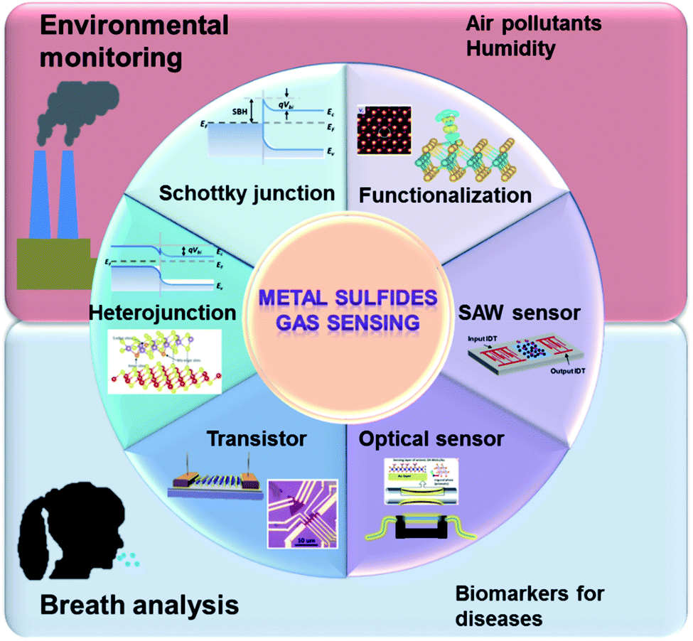
Lots of metal sulfide-based sensors can work at room temperature and have lower power consumption, making them superior to MOS-based sensors.27 The sensing performances of metal sulfides are similar to those of CNM-based devices, except for their sizeable and tunable bandgaps, making such materials suitable for transistor applications, further inducing unique sensing behaviours.28 They have the advantages of a shallow valence band, exposed active sites, and the quantum size effect. Typical metal sulfide semiconductors, such as molybdenum disulfide (MoS2) and tungsten disulfide (WS2), are layered metal disulfide materials, which consist of several S–metal–S layers attached via weak van der Waals (vdW) force. Sensor metal sulfide materials act as charge acceptors or donors. Because of the high-speed charge transfer and the high adsorption energy between it and gas molecules, metal disulfide has been widely used in gas sensing. The LOD of a MoS2 NO2 gas sensor is 20 ppb.29 For post-transition metal sulfide, tin sulfide (SnS) and germanium sulfide (GeS) are semiconductors that belong to a family of layered group IV monosulfides and have similar puckered structures to black phosphorus (BP).30–32 Owing to its anisotropic crystal structure, SnS has been employed for the detection of VOCs and toxic gases, such as acetone, alcohol, and NO2.33,34 Additionally, many advanced methods were proposed to improve their sensing properties, such as functionalizing metal sulfide (e.g., with defects or dopants), constructing heterojunctions (Schottky junctions and p–n, n–n, and p–p heterojunctions), and using transistors, see Fig. 2.
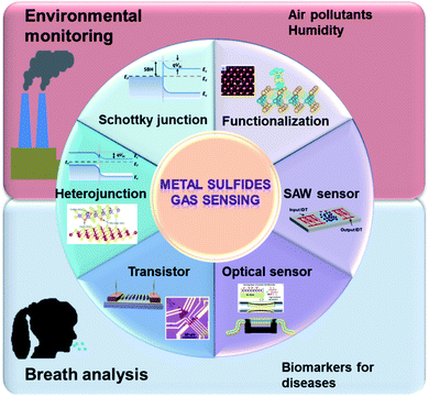 |
| | Fig. 2 Strategies of high-performance metal sulfide-based gas sensors and their applications. The heterojunction image is reprinted with permission from ref. 35 Copyright 2017, ACS Publishing. The functionalization images are reprinted with permission from ref. 36. Copyright 2013, ACS Publishing and reprinted with permission from ref. 37. Copyright 2017, Elsevier. The transistor image is reprinted with permission from ref. 38. Copyright 2013, ACS Publishing. The optical sensor image is reprinted with permission from ref. 39. Copyright 2020, ACS Publishing. | |
The present review will provide a comprehensive perspective on metal sulfide-based gas sensors, including the crystal structure, gas sensing mechanisms, applications, and perspectives. The paper is organized as follows: Section 2 describes the basic characteristics of metal sulfide nanomaterials. Section 3 discusses various gas sensing mechanisms of different metal sulfides through density functional theory (DFT). Section 4 summarises different sensing concepts of gas sensors based on metal sulfides. Section 5 lists the gas sensing applications of metal sulfide-based devices. Section 6 discusses the challenges and perspectives of metal sulfide sensors. This review is conceptually self-contained and intended to serve as an informational resource to newcomers and experienced researchers on metal sulfide-based sensors.
2. Gas sensing mechanisms of metal sulfides
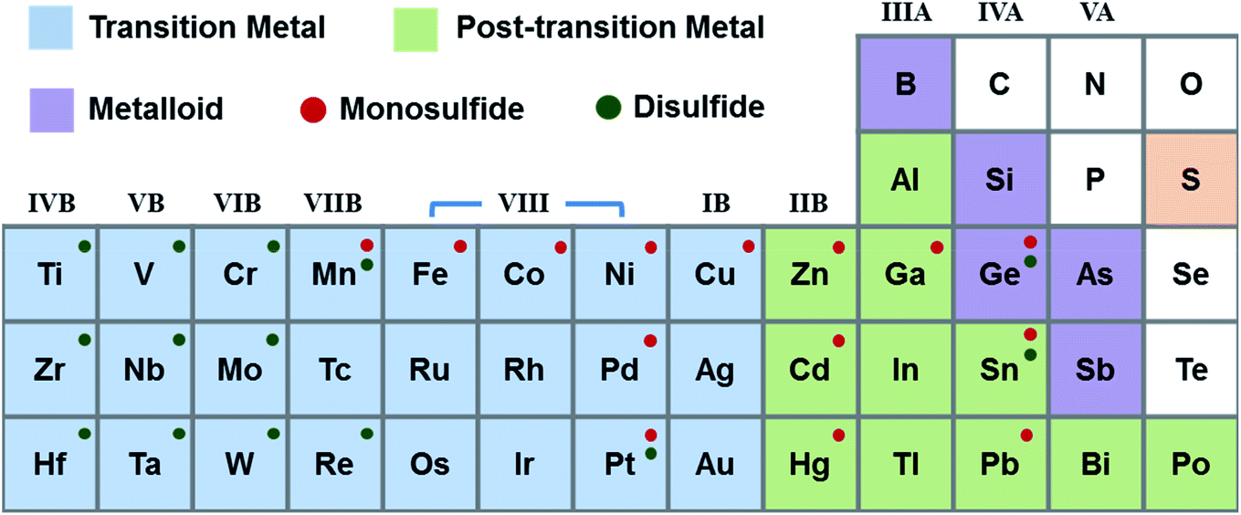
Sulfide is an inorganic sulfur anion with the chemical formula S2− or a compound containing one or more S2− ions.40 Metal sulfide is a kind of combination of sulfur anions and metal/semi-metal cations in the form of MxSy (x:y = 1:1, 1:2, 2:1, 3:4).41 As shown in Fig. 3, metal monosulfides mostly correspond to group VIII, IB, IIB, IIIA, and IVA metals. The elements from group IVB–VIIB and Sn can be used to form metal disulfides.42 Materials of the same composition with different crystal phases have different properties. 2H phase group VIB disulfides are usually semiconducting, while the corresponding 1T, 1T′, and Td phase crystals are metallic. Group IVA disulfides, such as GeS2 and SnS2, are often semiconductors. MoS2, WS2, and SnS2 are group VIB semiconductors, which have been used for transistors. Compared to other disulfides, group IVB disulfides exhibit high carrier mobility. Table 2 introduces the characteristics and applications of nanostructured metal sulfides. It is found that numerous metal sulfides possess several crystal phases, which can be controlled by altering the fabrication processes and external stimulations.41,43,44 The preparation strategies for metal sulfides primarily comprise “top-down” and “bottom-up” methods. The top-down approaches include sputtering, electrospinning, lithography, mechanical exfoliation (ME), and liquid phase exfoliation (LPE). Bottom-up strategies are chemical vapour deposition (CVD), atomic layer deposition (ALD), spray pyrolysis, pulsed laser deposition/ablation, thermal deposition, hydrothermal synthesis, solvothermal synthesis, and the self-assembly method. All these methods have been proposed to prepare large scale, high yield, and low-cost metal sulfides in the form of 0D, 1D, 2D, and 3D structures. Chandrasekaran et al.40 presented a comprehensive review on preparation technologies of metal sulfides; complementarily, in this review we primarily focus on gas sensing mechanisms and applications.
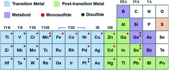 |
| | Fig. 3 Periodic table with symbols indicating metal sulfide. | |
Table 2 Characteristics and applications of nanostructured metal sulfidesa
|
|
Crystal structure |
Electric conductivity |
Bandgap [eV] |
Fabrication method |
Application |
Ref. |
|
Physical vapour deposition (PVD), chemical vapour transport (CVT).
|
| SnS |
Orthorhombic |
p-type |
Indirect 1.1 |
PVD |
Photodetectors, gas sensors |
45
|
| GaS |
Hexagonal |
Semiconductor |
Indirect 2.52 |
LPE |
Hydrogen evolution reaction |
46
|
| GeS |
Orthorhombic |
p-type |
(Monolayer) indirect 2.34 |
Vapour deposition |
High electron mobility |
32
|
| ZnS |
Hexagonal |
n-type |
Direct 3.7 |
Hydrothermal |
Gas sensors, optical sensors |
47
|
| CdS |
Hexagonal |
n-type |
Direct 2.42 |
Spray pyrolysis |
Solar cells, gas sensors |
48
|
| CuS |
Hexagonal |
p-type |
Direct 2.5 |
Deposition |
Solar cells, gas sensors |
49
|
| PbS |
Hexagonal |
n-type |
Bulk 0.373 nm 1.30 |
Chemical bath deposition |
Solar cells, photonics, gas sensors |
50 and 51
|
| NiS |
Rhombohedral |
p-type |
0.5 |
Solventless, thermal decomposition |
Photocatalysts |
52
|
| MoS2 |
2H hexagonal |
(2H) semiconductor |
(Bulk) indirect 1.29 |
CVD, ME |
FETs, photodetectors, solar cells, photonics, supercapacitors |
53 and 54
|
| 1T |
(1T) metal |
(Monolayer) direct 1.8 |
| WS2 |
2H hexagonal |
(2H) n-type |
(Bulk) indirect 1.3 |
CVD, ME |
FETs, photodetectors, gas sensors |
55
|
| 1T |
(1T) metal |
(Monolayer) direct 2.1 |
| SnS2 |
4H hexagonal |
n-type |
(Bulk) indirect 2.308 |
CVD, ME |
FETs, photovoltaics, photodetectors |
56
|
| (Monolayer) indirect 2.033 |
| ZrS2 |
1T rhombohedral |
n-type |
(Bulk) indirect 1.7 |
CVD |
Photoconductivity |
57
|
| HfS2 |
1T rhombohedral |
Semiconductor |
Indirect 2.0 |
ME |
FETs, phototransistors |
58
|
| NbS2 |
2H hexagonal |
Metal |
0.73 |
CVD |
Superconductivity |
59
|
| TaS2 |
1T rhombohedral |
Metal |
0.7 |
CVD |
Photosensitivity, superconductivity |
60
|
| 2H hexagonal |
| TiS3 |
Monoclinic |
n-type |
Direct 1.13 |
ME, CVT |
Photodetectors, gas sensors |
61 and 62
|
| ZrS3 |
Monoclinic |
n-type |
Direct 2.56 |
CVT |
Photodetectors |
63
|
| HfS3 |
Monoclinic |
Semiconductor |
— |
CVT |
FETs, photodetectors |
64
|
| TaS3 |
Orthorhombic |
Metal |
— |
— |
FETs, gas sensors |
65
|
| In2S3 |
Tetragonal |
n-type |
Direct 2.02 |
CVD |
Photodetectors, gas sensors |
66
|
It is demonstrated that the gas molecules physically or chemically adsorb at the surface of the nanostructured materials through adsorption energy. The higher the adsorption energy the stronger the adsorption interaction between gas molecules and metal sulfides. First-principles simulation, that is DFT calculations using plane waves and pseudopotentials, has become an efficient method to evaluate the sensing performance of 2D/nano-materials. Because the behaviours of atoms during chemical bonding and the flow of electrons in materials can be calculated through DFT based on quantum mechanics, it is much easier to understand the behaviour of systems at the atomic scale. This section discusses the major parameter calculated using DFT for evaluating sensing performance, the sensing mechanism of different metal sulfide materials, such as pristine, doped, defective, and heterojunction-based metal sulfides.
2.1 Performance parameters based on DFT results
First-principles calculations are performed to calculate the band structure, adsorption energy (Ea), charge transfer (ΔQ), bandgap (Eg), charge density difference (CDD), electron localization function (ELF), and density of states (DOS) of the gas molecule–metal sulfide system.
The Ea of gas molecules on a substrate can be calculated as,
| | | Ea = Ebare system + Egases − Etotal system | (1) |
where
Ebare system,
Egases, and
Etotal system are the total energies of the optimized bare metal sulfide, isolated gas molecules, and metal sulfide + gas molecule system, respectively. A negative value of
Ea indicates that the adsorption is exothermic. The higher the
Ea, the stronger the interaction between gas molecules and metal sulfides;
Ea has a great influence on the sensitivity/response of the chemiresistive gas sensor. Usually, the selectivity of materials can be determined through the
Ea among different types of gases, because the higher the
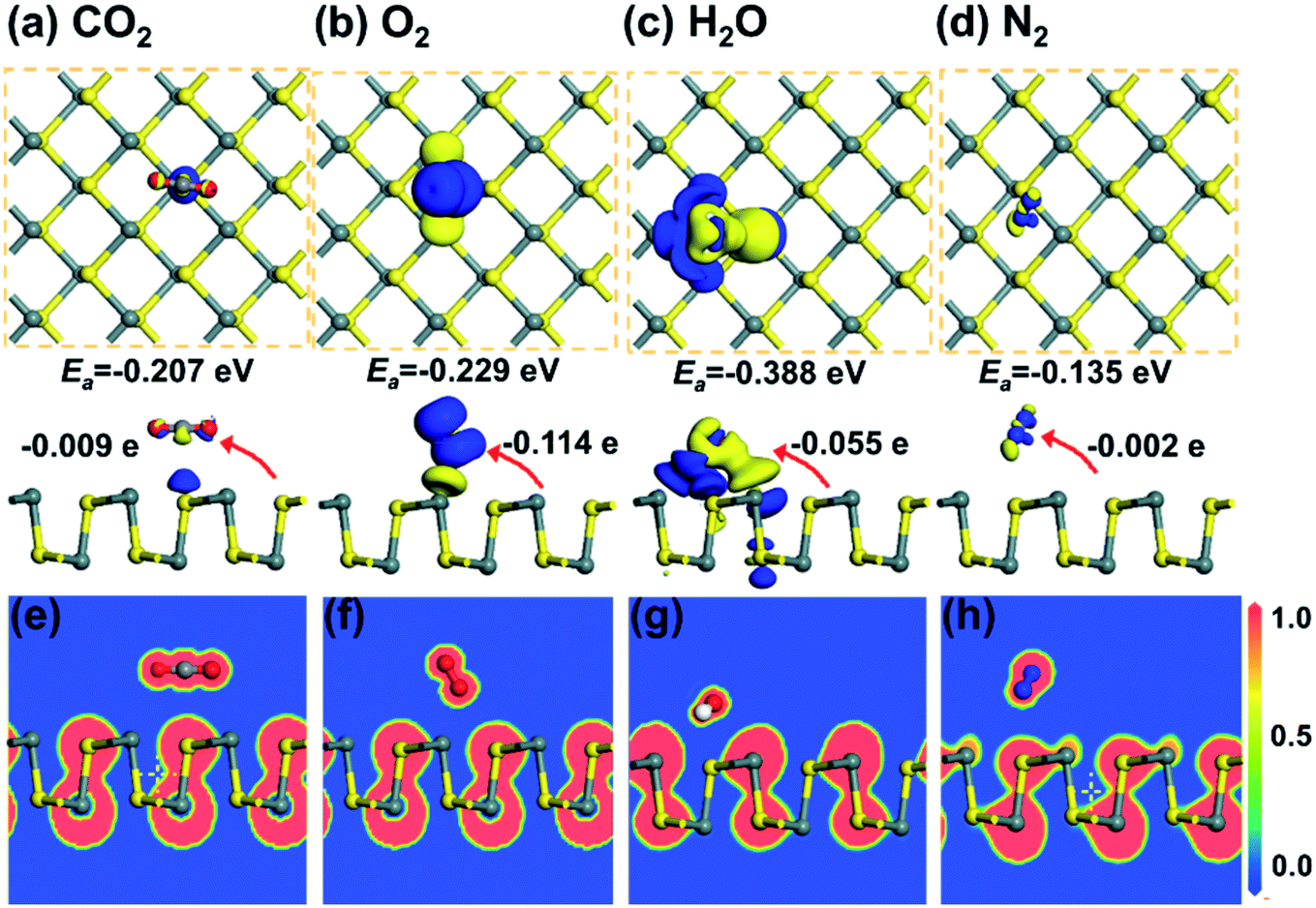
Ea, the higher the probability of adsorption towards the specific gas. As shown in
Fig. 4, the
Ea of the H
2O/SnS system is relatively high (−0.388 eV) among the four types of gases in air, which indicates that SnS has good sensitivity and specificity for the detection of H
2O in air.
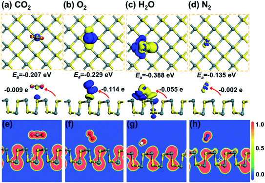 |
| | Fig. 4 The CDD for (a) CO2, (b) O2, (c) H2O, and (d) N2 adsorbed on monolayer SnS. The isosurface is taken as 0.003 e Å−3. (e)–(h) show the corresponding ELF plots. Reprinted with permission from ref. 71. Copyright 2019, © IOP Publishing. All rights reserved. | |
In addition to Ea, the electron transport property changes should also be considered. Charge transfer (ΔQ) is the total charge in the adsorbed gas molecule. It is shown as charge difference after DFT calculation, which can be calculated as follows:
| | | ΔQ = Qtotal system − Qbare system − Qgases | (2) |
where
Qtotal system,
Qbare system, and
Qgases are the total charge on metal sulfide + gases, metal sulfide, and gas molecules, respectively. The amount of charge transferred was calculated by Löwdin analysis.
67 Some typical CDD images are shown in
Fig. 4a–d. The blue region represents charge accumulation, while the yellow region shows charge depletion. These four types of gas molecule (CO
2, O
2, H
2O, and N
2) act as charge acceptors and receive electrons of 0.009
e, 0.114
e, 0.055
e, and 0.002
e from SnS, respectively.
In quantum chemistry, ELF is a measure of the possibility of finding an electron in the neighborhood space of a reference electron at a given point and with the same spin.68 The ELF provides a method for mapping the electron pair probability in multielectronic systems and a description of electron delocalization in molecules and solids.69 It can be used to analyze the extent of spatial localization of the reference electron and classify the chemical bond for almost all classes of compounds.70 The ELF plots are normalized and present as a jellium-like homogeneous electron. The normalized values of 1.00, 0.50, and 0.00 refer to fully localized electrons, fully delocalized electrons, and very low charge density, respectively. Some typical ELF images are shown in Fig. 4e–h. It is found that there is no remarkable electron sharing between gas molecules and SnS, which indicates that the chemical bond is unformed.
The DOS of a system presents the features of the electronic structure, such as the bandgap in insulators and the width of the valence band. It helps to qualitatively analyze the effects of external stimulations on the electronic structure, such as molecules, pressure, mechanical strain, and electric field. Fig. 5a shows the total DOS of the adsorption system of SnS without and with NH3. The DOS of the SnS system changes slightly after adsorbing NH3 molecules, which is associated with the electronic level localized between −4 eV and −2 eV in the valence band. However, concerning the NO2/SnS system, there are obvious changes of the DOS on both sides near the Fermi level, which reveals the strong interaction between NO2 and SnS (Fig. 5b).
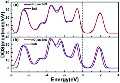 |
| | Fig. 5 The total DOS for (a) NH3 and (b) NO2 adsorbed on monolayer SnS. The Fermi level is set as zero. Reprinted with permission from ref. 72. Copyright 2017, IEEE. | |
2.2 Gas sensing mechanisms
2.2.1 Pristine metal sulfides.
N-type and p-type metal sulfides.
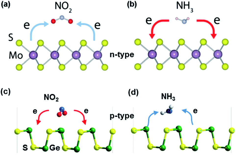
When exposed to gases, the charge transfer reaction occurs between the sensing materials and the adsorbed gases, accompanied by different transfer directions and quantities of charges, which leads to different changes in the material resistance. If the sensing materials are re-exposed to air, desorption of gas molecules occurs, causing the sensing material resistance to return to its initial state.73 As shown in Fig. 6, when n-type MoS2 is exposed to oxidizing gases such as O2, H2O, NO, NO2, and CO, the electron charges transfer from MoS2 to the sensitive gases, leading to a decreased carrier density in MoS2. As a result, the resistance of n-type MoS2 increases. In contrast, reducing (NH3) gas molecules adsorbed on MoS2 act as charge donors and transfer electrons to the MoS2 monolayer, increasing the electron carrier density of the n-type MoS2 monolayer and reducing its resistance.74 Among post-transition metal sulfides, GeS is a p-type semiconductor, where the electron-accepting gases act as charge donors to GeS and NH3 molecules trap electrons from GeS. Besides, lots of DFT calculations proved that gas molecules adsorb more strongly at the edge sites than at the basal plane of metal sulfides.75,76
 |
| | Fig. 6 Gas sensing mechanism of (a and b) MoS2 (n-type metal sulfide). Reprinted with permission from ref. 27. Copyright 2018, ACS Publishing. (c and d) GeS (p-type metal sulfide) in the presence of NO2 and NH3 molecules. Reprinted with permission from ref. 77. Copyright 2018, The Royal Society of Chemistry. | |
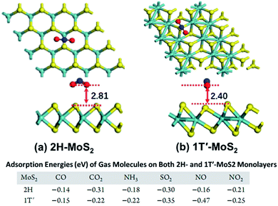 |
| | Fig. 7 Top and side view of the most stable configurations of NO2 molecules adsorbed on (a) 2H–MoS2 and (b) 1T′-MoS2. The distance (Å) between the molecule (the lowest atom) and the MoS2 sheets (the plane of the uppermost S atoms) is labelled. The bottom table shows the Ea of different gases on the 2H–MoS2 and 1T′-MoS2 monolayer. Reprinted with permission from ref. 79. Copyright 2019, ACS Publishing. | |
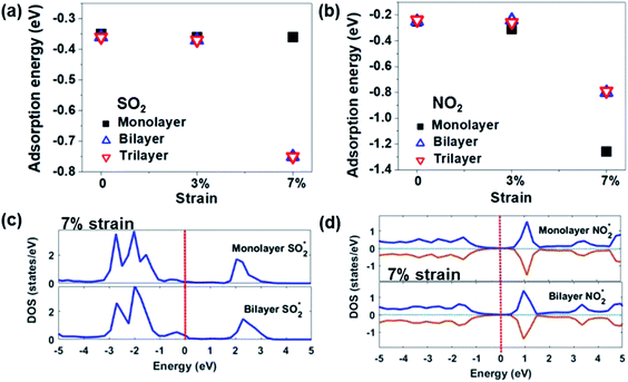 |
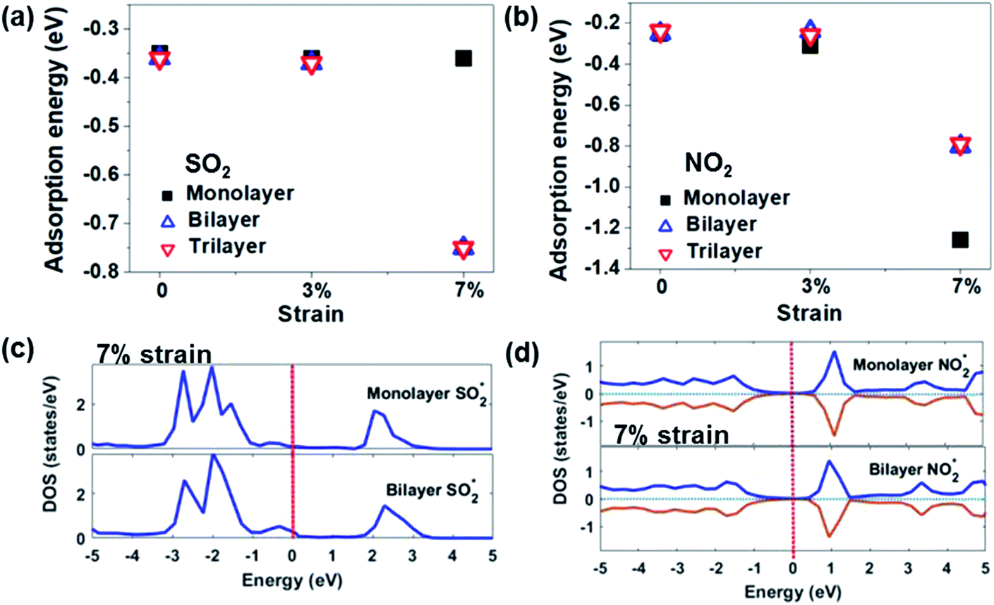
| | Fig. 8 Adsorption energies of (a) SO2 and (b) NO2 on 1T′-MoS2 sheets with a different number of layers and different strains. Total DOS of MoS2 monolayer and bilayer systems at 7% strain adsorbed by (c) SO2 and (d) NO2. Reprinted with permission from ref. 79. Copyright 2019, ACS Publishing. | |
 |
| | Fig. 9 The schematic of the interfacial interaction between the surface and interlayer of WS2 and NH3 molecules. Reprinted with permission from ref. 81. Copyright 2017, Elsevier. | |
2.2.2 Doped metal sulfides.
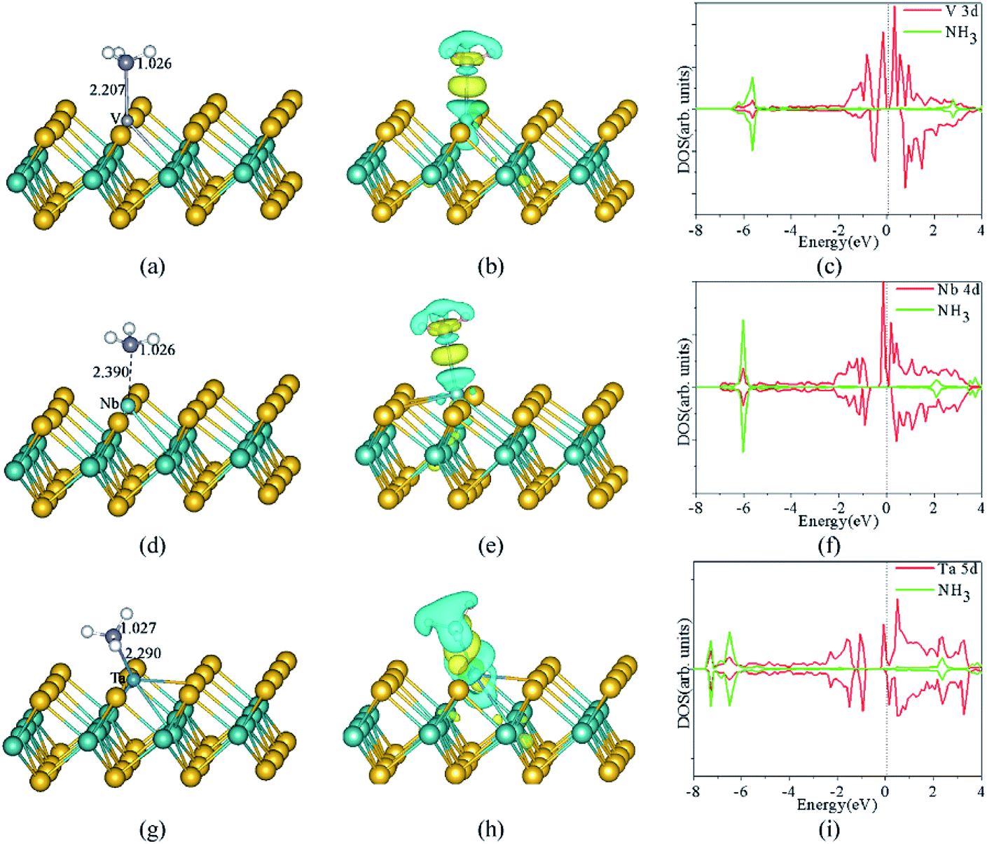
Chemical doping is an efficient way to change the band structure, modify the electronic and transport properties, and enhance the gas sensing applications. Metal doping is the most common method used for metal sulfides. Fig. 10 shows that typically doped metal atoms (i.e., V, Nb, and Ta) replace the Mo atoms of metal sulfides. Table 3 lists the different types of metal dopants for monolayer MoS2, such as Al, Si, P, Ni, Cu, Au, Pt, Pd, V, Nb, Ta, B, N, Fe, Co, and AuxCuy, and their Ea after adsorbing different gas molecules (NOx, CO, NH3, SO2, H2S, SF6, O2, H2, carbonyl fluoride (COF2), cobalt tetrafluoride (CF4), and H2O). Based on the DFT results of all the metal-doped MoS2 listed in Table 3, Ta-doped MoS2 has the highest Ea of 4.30 eV towards NO2, 1.78 eV towards CO, and 1.65 eV towards H2O; Si-doped MoS2 shows a high Ea of 2.156 eV to NH3; Al-doped MoS2 shows an Ea of 2.33 to SO2. Besides, Li et al.84 demonstrated that Ni-doped MoS2 has great potential for sensing applications in organic gas molecules, such as COF2 and CF4.
 |
| | Fig. 10 The optimized structures, CDD, and corresponding spin-polarized DOS projected on 3d states of V atoms, adsorbed gas molecules of NH3 adsorbed on the monolayer MoS2 with V (a, b and c), Nb (d, e and f), and Ta (g, h and i) doped in the S-vacancy, respectively. The Mo, S, N, H, V, Nb, and Ta atoms are denoted by dark green, yellow, purple, white, light grey, light green, and blue spheres, respectively. The yellow and cyan regions represent the positive (electron accumulation) and negative (electron depletion) values, respectively. The isosurface value is taken as 0.003 e Å−3. The vertical dashed line indicates the position of the Fermi level, taken as zero energy. Reprinted with permission from ref. 37. Copyright 2017, Elsevier. | |
Table 3 Literature study on the Ea of doped metal sulfide nanomaterials with different gas molecules
| Material |
Type of doping |
NO2 |
NO |
CO |
NH3 |
SO2 |
H2S |
SF6 |
O2 |
H2 |
COF2 |
CF4 |
H2O |
Ref. |
| MoS2 |
Pristine |
−0.069 |
— |
— |
−0.063 |
— |
— |
— |
— |
— |
— |
— |
— |
85
|
| Al-doped |
−3.02 |
— |
— |
−2.116 |
— |
— |
— |
— |
— |
— |
— |
— |
| Si-doped |
−2.588 |
— |
— |
−2.156 |
— |
— |
— |
— |
— |
— |
— |
— |
| P-doped |
−2.134 |
— |
— |
−0.34 |
— |
— |
— |
— |
— |
— |
— |
— |
| Ni-doped |
— |
— |
— |
— |
−1.382 |
−1.319 |
−0.181 |
— |
— |
— |
— |
— |
86
|
| Ni-doped |
— |
— |
— |
— |
— |
— |
— |
— |
— |
0.723 |
0.265 |
— |
84
|
| Pristine |
— |
0.11 |
0.07 |
— |
— |
— |
— |
— |
— |
— |
— |
— |
87
|
| Cu-doped |
— |
1.25 |
1.44 |
— |
— |
— |
— |
— |
— |
— |
— |
— |
| Au-doped |
— |
1.08 |
0.91 |
— |
— |
— |
— |
— |
— |
— |
— |
— |
88
|
| Pt-doped |
— |
1.21 |
1.38 |
— |
— |
— |
— |
— |
— |
— |
— |
— |
| Pd-doped |
— |
0.93 |
0.96 |
— |
— |
— |
— |
— |
— |
— |
— |
— |
| Ni-doped |
— |
1.62 |
1.38 |
— |
— |
— |
— |
— |
— |
— |
— |
— |
| V-doped |
3.08 |
— |
1.39 |
1.54 |
— |
— |
— |
— |
— |
— |
— |
1.12 |
37
|
| Nb-doped |
4.30 |
— |
1.46 |
1.43 |
— |
— |
— |
— |
— |
— |
— |
0.99 |
| Ta-doped |
4.05 |
— |
1.78 |
1.95 |
— |
— |
— |
— |
— |
— |
— |
1.65 |
| Pristine |
— |
— |
— |
— |
−0.36 |
— |
— |
— |
— |
— |
— |
— |
89
|
| B-doped |
— |
— |
— |
— |
−1.17 |
— |
— |
— |
— |
— |
— |
— |
| N-doped |
— |
— |
— |
— |
−0.58 |
— |
— |
— |
— |
— |
— |
— |
| P-doped |
— |
— |
— |
— |
−0.51 |
— |
— |
— |
— |
— |
— |
— |
| Al-doped |
— |
— |
— |
— |
−2.33 |
— |
— |
— |
— |
— |
— |
— |
| Pristine |
— |
— |
— |
— |
−0.209 |
— |
— |
— |
— |
— |
— |
— |
90
|
| Ni-doped |
— |
— |
— |
— |
−0.835 |
— |
— |
— |
— |
— |
— |
— |
| Fe-doped |
— |
— |
— |
— |
−0.218 |
— |
— |
— |
— |
— |
— |
— |
| Co-doped |
— |
— |
— |
— |
−0.213 |
— |
— |
— |
— |
— |
— |
— |
| Au-doped |
— |
— |
1.16 |
— |
— |
— |
— |
— |
— |
— |
— |
0.41 |
91
|
| Cu-doped |
— |
— |
1.31 |
— |
— |
— |
— |
— |
— |
— |
— |
0.68 |
| AuCu-doped |
— |
— |
1.13 |
— |
— |
— |
— |
— |
— |
— |
— |
0.61 |
| Au2Cu2-doped |
— |
— |
1.25 |
— |
— |
— |
— |
— |
— |
— |
— |
0.71 |
| Au3Cu3-doped |
— |
— |
1.23 |
— |
— |
— |
— |
— |
— |
— |
— |
0.63 |
| WS2 |
Pristine |
— |
0.25 |
0.21 |
— |
— |
— |
— |
0.22 |
— |
— |
— |
0.23 |
92
|
| −0.354 |
−0.206 |
−0.127 |
−0.216 |
— |
— |
— |
−0.213 |
−0.075 |
— |
— |
−0.229 |
93
|
2.2.3 Defective metal sulfides.
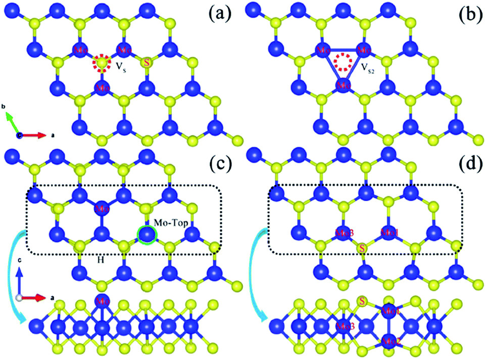
It is known that the MoS2 monolayer exhibits naturally formed vacancies, such as S vacancies (VS) and Mo vacancies (VMo), which have significant impacts on the gas sensing performance.94–97 Zhao et al.94 investigated various defects in monolayer MoS2, including monosulfur vacancies (VS), disulfur vacancies (VS2), Mo vacancies (VMo), a vacancy complex of Mo with three (VMoS3) or six (VMoS6) nearby sulfur vacancies, antisite defects where a Mo atom is substituting a sulfur atom (MoS) or an S2 column (MoS2), antisite defects where a sulfur atom (SMo) or S2 column (S2Mo) substitutes a Mo, and an external Mo (Mo–In). They found that four types of defect systems were stable after geometry optimizations, as shown in Fig. 11. These are monosulfur vacancies (MoS2–VS), disulfur vacancies (MoS2–VS2), antisite defects (MoS2–MoS), and external Mo atoms (MoS2–Mo). The corresponding Ea values after adsorbing O2 are −1.822, −1.687, −3.293, and −2.545 eV for MoS2–VS–O2, MoS2–VS2–O2, MoS2–MoS–O2, and MoS2–Mo–O2, respectively. All of them are much stronger than that of pristine MoS2 (−0.01 eV). The CDD results reveal typical chemisorption of O2 on the defective surface, which is associated with the O–O bond length extension in varying degrees.
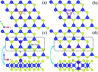 |
| | Fig. 11 Optimized geometric structure of the defect within a monolayer MoS2: (a) monosulfur vacancy (VS), (b) disulfur vacancy (VS2), (c) antisite MoS, and (d) an external Mo located on the top of the Mo lattice site. Reprinted with permission from ref. 94. Copyright 2017, Elsevier. | |
2.2.4 Metal sulfide-based heterojunctions.
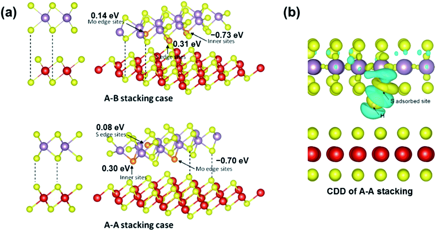
Different stacking methods affect the Ea of the gas/substrate system. As shown in Fig. 12a, MoS2/VS2 heterojunctions with A–B and A–A stacking are built and used to investigate their hydrogen evolution ability.35 The Gibbs free energies of the inner sites and Mo and S edge sites of the A–B and A–A stacking cases were also compared. The corresponding energies were calculated to be −0.73, 0.14, and 0.31 eV for the A–B stacking cases and −0.70, 0.08, and 0.30 eV for the A–A stacking cases. The difference of energies in these two stacking cases is associated with the bandgap barrier from VS2 to MoS2, which induces different internal charge transfer. The CDD image in Fig. 12b further proves the charge transfer between the adjacent H atoms and the S atom. There is still a lack of DFT simulation results of the gas molecule/heterojunction system for metal sulfides. Lots of experimental results are analyzed based on bandgap theory, which will be described in the next section.
 |
| | Fig. 12 (a) Two types of stacked bilayer structural models and their adsorption configurations. (b) CDD of the A–A stacking case (right) of the VS2@MoS2-edge nanosheet. The cyan and yellow regions represent the charge depletion and accumulation space, respectively. Reprinted with permission from ref. 35 Copyright 2017, ACS Publishing. | |
3. Various sensing concepts of metal sulfide-based devices
Based on the gas sensing mechanism, metal sulfide-based devices can be classified into chemiresistors, Schottky junctions, heterojunctions, field-effect transistors (FETs), and optical and surface acoustic wave (SAW) gas sensors. In this section, we introduce the performance parameters as well as the sensing concepts of these devices.
3.1 Performance parameters
Typically, the criteria of an efficient gas sensor consist of high sensitivity and selectivity, fast response and recovery time, long-term stability, and low power consumption. Here, a set of parameters is defined to evaluate and compare the performance of different sensors, including response, sensitivity, selectivity, LOD, dynamic range, response and recovery time, and stability.
3.1.1 Response.
The response is defined as the change in measured current (I), resistance (R), capacitance (C), conductance (G = I/V), light power (P), effective refractive index (RI), and resonant frequency (f) for a given gas concentration unit concerning the signal in the absence of analyte molecules. It is defined as:| | | (Xgas − X0)/X0 = ΔX/X0 | (3) |
where X = I, R, C, G, P, RI, or f, Xgas is the sensor's signal after adsorbing the analyte gas, and X0 is the baseline signal (no analyte gas). Different concentrations of the analyte gas could induce different responses. This review uses response in percentage (response%) = response × 100% to present the change of the testing signal.
3.1.2 Sensitivity.
Sensitivity is defined as the capability to discriminate small differences in concentration or mass of the analyte. In other words, the sensitivity of the sensor is the slope of the calibration graph, which represents the variation in the sensor response per unit concentration of the target gas. In other words, sensitivity (S) = response/concentration. Thus, a higher sensitivity indicates a higher efficiency of the sensor.
3.1.3 Selectivity.
Selectivity refers to the strong adsorption of target gases in the mixed gas, while being insensitive to other gases. The selectivity factor/coefficient (K) of the ‘target gas’ to another gas is defined as:where S1 and S2 are the sensitivities of the sensor to a target gas and another gas, respectively.
LOD is a key figure of merit in chemical sensing, used as an indicator of the minimum concentration of a detectable analyte.98 Traditionally, LOD formulas, according to the International Union of Pure and Applied Chemistry (IUPAC), are based on the use of linear regression models.98 When the signal is three times greater than the noise, the theoretical LOD can be calculated from the slope of the linear region of the response curve, namely “Sensitivity (S)” and the root-mean-square (RMS) deviation at the baseline,
where RMS
noise is the noise level in the absence of the analyte gas. Concerning the LOD in non-linear gas sensors, including metal oxide sensors, gas FETs, or thermoelectric sensors, Burgués
et al.99 proposed a methodology to estimate LOD through linearized calibration models.
Operating temperature (OT) is the temperature that corresponds to maximum sensitivity.
3.1.4 Response and recovery time.
The response time (τs) and recovery time (τr) are defined as the time required for reaching 90% of the final response and the time taken to recover 90% of the original value of the device. They are mostly used as an index of the speed of response, which is highly dependent on the types of gases, the device structure, and the exposure time.
Stability is defined as the ability of a sensor to provide consistent and reproducible results for a specified period. This parameter becomes highly important when sensors are exposed to hazardous, corrosive, or high-temperature atmospheres.
Usually, an ideal gas sensor would possess high sensitivity, selectivity and stability, low LOD, and short recovery and response times. But its final application depends on the requirements of the specified environment or working conditions. Moreover, all the parameters could be affected by other factors, including the sensing materials, substrate, environmental factors (temperature, humidity, and pressure), and testing setup (volume, shape, and gas flow rate).
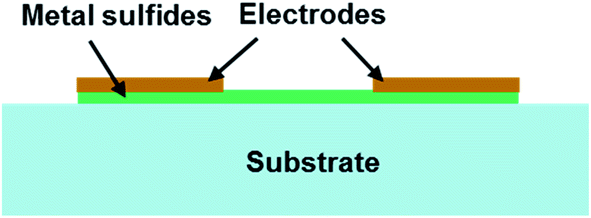
3.2 Chemiresistor gas sensors
Typically, different types of metal sulfides, such as nanoflakes (NFKs), nanosheets (NSs), nanowires (NWs), nanorods (NRs), nanoflowers (NFWs), or nanotubes (NTs), are synthesized or transferred on a substrate (i.e., sapphire, Si, and SiC) to form a chemiresistor sensor, as shown in Fig. 13. The electrodes can be pre-made on the substrate or evaporated on the top of metal sulfides after the transfer process.
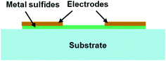 |
| | Fig. 13 Schematic of the structure of a metal sulfide-based chemiresistor gas sensor. | |
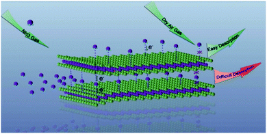
As mentioned in Section 2.2, the basic sensing principle is metal sulfides act as charge acceptors or donors. Their shallow valence band, small effective mass, and diverse structures enable a quantum size effect and promising applications in gas sensing. The typical direct narrow bandgap IV–VI compound semiconductors, such as SnS, PbS, and GeS, have similar puckered structures to black phosphorus.30,31 They have been employed for the detection of toxic (NO2, NH3, and H2S) and organic (e.g., acetone and ethanol) gas molecules. The response and recovery time is fast (5–36 s).33,100,101 The II–VI compound semiconductors mostly have a direct wide bandgap, including CdS and ZnS. They have high response and selectivity to VOCs, including isopropanol, methanol, ethanol, acetone, and methylbenzene. However, their OTs are relatively high (200–300 °C).102,103 Other metal monosulfide-based gas sensors, such as CuS and NiS, also have potential applications in H2 and SO2 gas sensing.104–106 According to Kim's research, 75% of publications up to 2017 were focused on MoS2 followed by WS2 (14%) and SnS2 (9%).13 The predominance of MoS2 over other metal disulfides is because this material is the easiest to synthesize and the most stable among transition metal sulfides. Most transition metal sulfides are composed of metal atoms sandwiched between two layers of hexagonally close-packed sulfur (S) atoms; the adjacent S layers are connected by the weak van der Waals forces. They have a larger electronegativity, potentially increasing the number of gas adsorption sites. Thus various transition metal sulfides, including NbS2, ReS2, TaS2, and VS2, were used for gas sensing in NOx, NH3, O2, and ethanol.
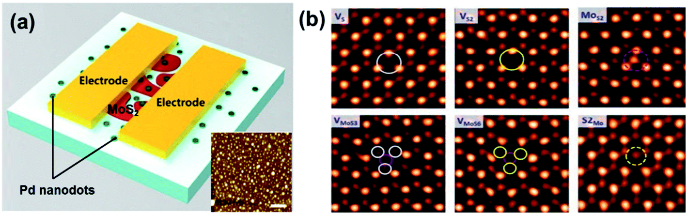
Functionalization is a versatile method for the modulation of the electronic and chemical properties of metal sulfides. As discussed in Section 2.2, doping and defect substitution are the most commonly used tools in functionalization, which can change the electronic structure, modify chemical reactivity, and affect the sensing performance.108Fig. 14 shows a hydrogen sensor with few-layered Pd-doped MoS2 and various point defects in CVD-MoS2.36,107 Qin et al.109 demonstrated an enhanced NH3 sensor based on 2D SnS2 with sulfur vacancies. It showed a fast response time of 16 s toward 500 ppm NH3. The enhanced sensitivity is associated with the high Ea of the defective system of 2D SnS2. However, most of the gas-sensing behaviours of functionalized metal sulfides were analyzed through DFT calculations. There are a lack of experimental reports on the influence of defects on the metal sulfide-based devices' gas-sensing performance.
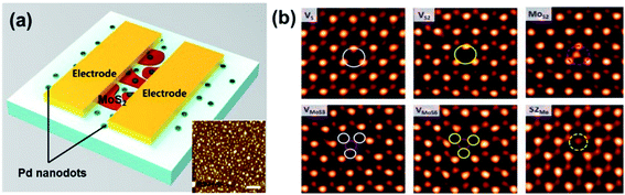 |
| | Fig. 14 (a) Schematic of a Pd-doped MoS2-based sensor. The inset image shows the AFM image of Pd on a SiO2 substrate. The scale bars indicate a distance of 400 nm. Reprinted with permission from ref. 107. Copyright 2017, Elsevier. (b) Image analysis for intrinsic point defects in ML MoS2. Reprinted with permission from ref. 36. Copyright 2013, ACS Publishing. | |
3.3 Schottky junction
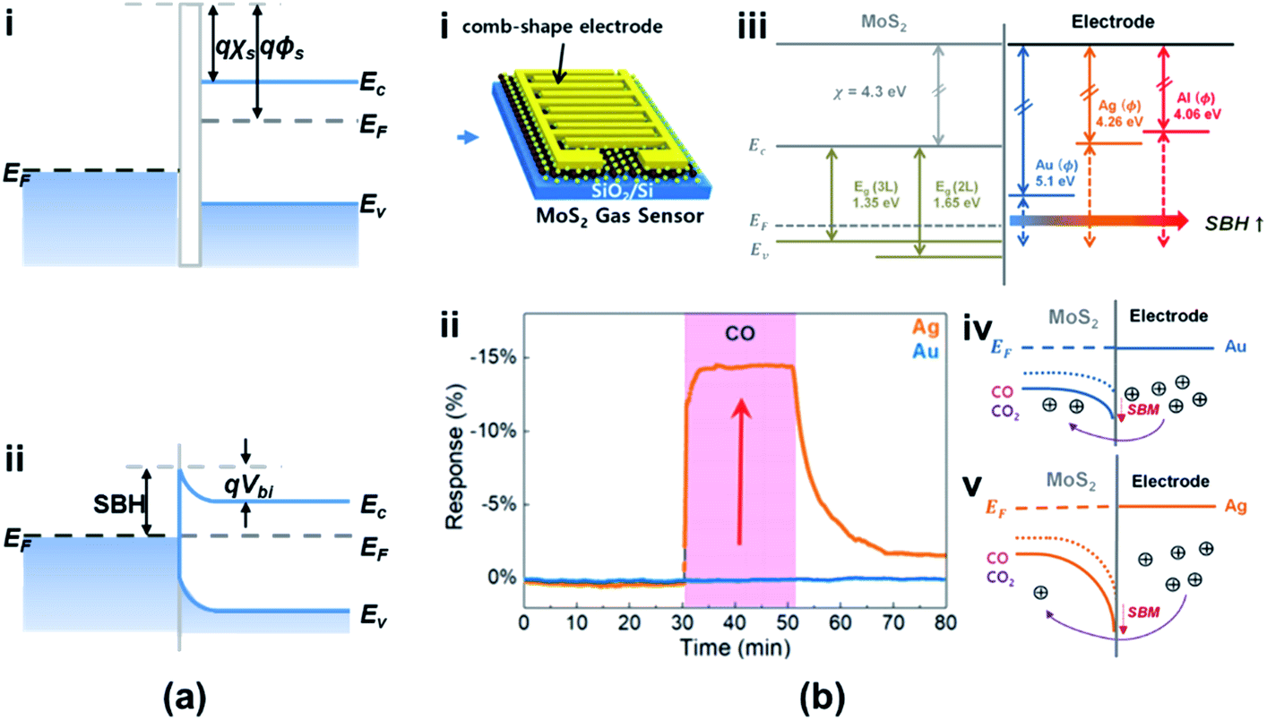
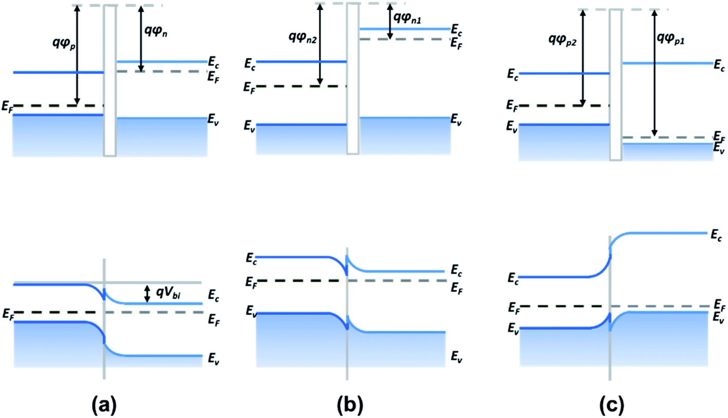
Typically, a metal–semiconductor (M–S) junction is a type of heterostructure where a metal is in close contact with a semiconductor material. The rectifying M–S junction is called a Schottky junction, while the non-rectifying junction forms an ohmic contact. Recently, researchers reported that a Schottky or an ohmic contact can also be formed between an atomic CNM and a semiconductor, depending on their electron affinity values.8Fig. 15a shows a typical Schottky junction, in which the electrons flow from the conduction band to the semiconductor layer until they reach equilibrium. This forms a Schottky barrier (SB) of the built-in potential barrier (Vbi) in the contact layer and hinders further charge transport.110 The Schottky barrier height (SBH) from the metal side remains unchanged, while the bias across the junction could change according to the work function of the semiconductor (φs). As shown in Fig. 15b(i–v), the SBH was controlled using different metals (Au, Ag, and Al) as the materials of electrodes. The adsorbed gas molecules, i.e., COx, are a kind of dopant for the semiconductor, which could modify the doping level of materials and modulate the φs in turn (see Fig. 15b(iv and v)).111 The SB is determined from the difference between φm and φs, strongly influenced by the gas molecules. Therefore, the SBH is easily varied owing to the change of the gas concentration. Fig. 15b(ii) shows that the response to CO gas is improved in devices after using the Ag electrode due to the increase in SBH, which means that the Schottky contact sensor could improve the sensitivity because the modulations of the φB0 and barrier width in the Schottky junction by gas molecules are concentrated in the tiny area of contact between the metal and metal sulfides and the Schottky diode-based sensor can detect ultralow levels.112,113 Besides, the sensing performances of vdW vertical heterojunctions of CNMs and metal sulfides are not only associated with the SBH modulation mechanism but also with the abundant adsorption sites on the CNMs' surfaces. This enables a significant enhancement of the device sensitivity toward the ppb level of NO2 gas exposure reaching 4.9%/ppb (4900%/ppm).114
 |
| | Fig. 15 Band alignment of (a) the Schottky junction. Ec, EF, and Ev are the conduction band edge, Fermi level, and valence band edge of the semiconductor, respectively. φm, φs, and χs are the metal work function (measured in volts), the semiconductor work function, and electron affinity, respectively. φB0, Vbi, and xn are the barrier height, built-in potential barrier, and depletion width, respectively. Other symbols have their usual meaning. (b) (i) Schematic of the metal-MoS2 Schottky contact gas sensor. (ii) Sensing characteristics of CO for 2 L MoS2 with Au and Ag electrodes. (iii) Band diagram of MoS2 with metal electrodes. Band alignment of (iv) the Au/MoS2 gas sensor and (v) Ag/MoS2 gas sensor before and after CO and CO2 exposure. Reprinted with permission from ref. 111. Copyright 2019, ACS Publishing. | |
3.4 Heterojunction based gas sensors
Heterojunctions based on metal sulfide can be easily constructed and present superior electric and photoelectric properties compared to pristine metal sulfide owing to the abundant adsorption sites and unique interface state at the contact interface.115 According to the type of semiconductors, 2D heterojunctions can be classified as p–n, n–n, and p–p junctions.
3.4.1 p–n junction.
The band alignment of a p–n heterojunction is shown in Fig. 16a; electrons and holes flow in opposite directions until equilibrium is achieved, forming a thick space-charge region that further narrows the electrical transport channels. Mostly, in p–n heterojunction gas sensors, the sensing performances are determined by the difference in the areal coverage of the two dissimilar materials as well as the interfacial bonds.41,117 With a higher areal coverage of the material, more electrons flow through the material, and so the charge transfer between gas molecules and the material is stronger than in the case of the material with lower areal coverage. Higher area materials dominate the sensing response of the p–n heterojunction. Concerning the interfacial states of a p–n junction, there are many dangling bonds and voids in the interface owing to a random connection between two different crystals.118 Since dangling bonds could trap the electron in the conduction path, the charge transfer is impeded, requiring additional energy to drive the electrons across the electron-depletion layer (EDL). Therefore, it is recommended to keep the interface state at a low density, for instance, by adopting lattice-matched materials or enhancing the crystal quality of the materials. Through the hydrothermal method, MoS2/SnO2 p–n heterojunctions have been fabricated and used for ethanol, trimethylamine (TMA), and NO2 gas sensing.119–121 They exhibited high sensitivity, lower OT, excellent sensing selectivity, and outstanding long-term stability. However, there are still a lack of quantitative experimental and theoretical analyses of the effects of areal coverage and dangling bonds on the gas sensing performances.
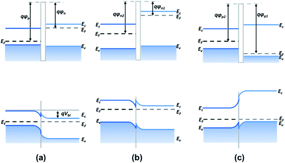 |
| | Fig. 16 Band alignment of (a) p–n junctions, (b) n–n junctions, and (c) p–p junctions. Ec, EF, and Ev are the conduction band edge, Fermi level, and valence band edge of the semiconductor, respectively. φp, φn, and Vbi are the p-type semiconductor work function, the n-type semiconductor work function, and the built-in potential barrier, respectively.116 | |
3.4.2 n–n or p–p junction.
Recently, various n–n and p–p heterostructures have been proposed to improve the gas-sensing performances. Most of the n–n and p–p junction gas sensors are based on metal oxide nanomaterials, such as SnO2/TiO2,122 SnO2/ZnO,123 SnO2/Sn3O4,124 TiO2/ZnO,125 CaO/ZnO,126 ZnO/In2O3,127 and CuO/rGO,128 whose enhanced performances are attributed to the heterocontact of the two semiconductor surfaces. For metal sulfide-based n–n and p–p heterojunctions, Zhang et al.129 optimized the NH3 sensing behaviour by using SnS2/ZnS hierarchical NFWs. The gas sensors based on metal sulfide n–n junctions benefiting from metal oxide hybrids, such as CdS/CeO2,130 CdS/ZnO,131 ZnS/ZnO,132 and ZnS/CuO,133 have been employed for the detection of VOC toxic gases. The electrons flow across the heterojunction from the higher Fermi level to the lower one, which induces band bending and EDL formation at the interface. This improves the transfer efficiency of the interfacial charge and increases the adsorption of oxygen species. An EDL and electron-accumulation layer (EAL) are formed at n–n (Fig. 16b) and p–p (Fig. 16c) heterointerfaces. The adsorbed gases on the surface could further influence the width of the EDL/EAL by extracting/giving electrons from/to the conduction band of the semiconductors. Therefore, the conductivity of the device could be altered with the type and the concentration of analytes (gas molecules). Moreover, the interface states of n–n or p–p heterojunctions need further experimental and theoretical analysis.
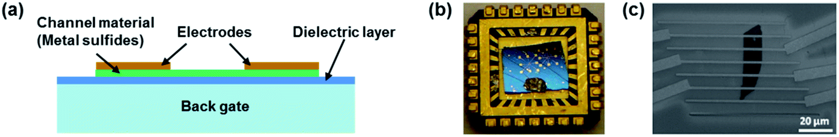
3.5 FET gas sensors
FET gas sensors have attracted much research interest because of their sensitive detection and miniaturization.134,135Fig. 17 shows a typical FET gas sensor consisting of a sensing semiconductor as a channel material, a back gate layer, a dielectric layer, and source and drain electrodes on the two ends of the channel material. The conductance of the channel can be modulated by applying different bias voltages on the gate electrode through a thin dielectric layer.8 The channel materials could be pristine or functionalized metal sulfides and metal sulfide-based heterojunctions. Similarly to the chemiresistor gas sensor, gas detection can be realized by measuring the change of the current between the source and drain (Ids) before and after exposure to target gases. The primary difference is that the gate voltage could alter the channel's charge carrier concentration by modulating the electric field across the dielectric layer. Consequently, the charge transfer between channel and target gases could be modified in the form of changes in the Ids. Traditionally, FET sensors could be back-gate FETs and top-gate FETs; however, most FET gas sensors are back-gate FETs because the channel materials can directly come into contact with target gases. This type of sensing device has been used to detect many types of gases, such as CO, NO, NH3, NO2, SO2, H2, and VOCs. However, most FET gas sensors are still not satisfactory due to their device instability and limited large-scale production even though they exhibit fast response and high selectivity.136
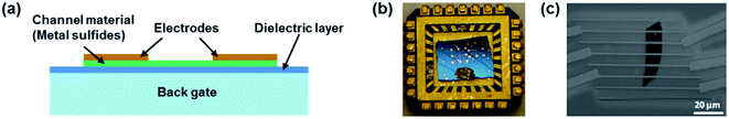 |
| | Fig. 17 (a) Schematic of an FET gas sensor. (b) Optical image of the MoS2 transistor sensor on a chip. (c) SEM image of a two-layer MoS2 transistor. Reprinted with permission from ref. 83. Copyright 2013, ACS Publishing. | |
3.6 Optical gas sensors
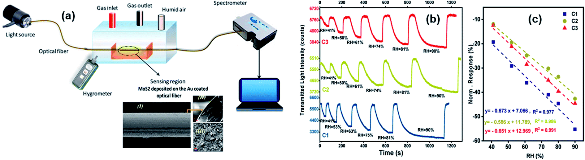
Optical gas sensors monitor the optical properties of different gas species at defined optical wavelengths. They can be used as an optical “fingerprint” for any gas species because different types of gases have a specific distribution of optical absorption/emission with the wavelength. Besides, different changes in optical properties of sensors can reflect different gas concentrations. Metal sulfides have strong photoluminescence, a wide range of photoresponsivity, high carrier mobility, and high sensitivity to humidity variation.4,40 Fibre-optic sensors are attractive due to their low cost, light weight, and anti-corrosion properties.137 Therefore, taking advantage of the superior properties of both metal sulfides and optical fibres was considered. Most of metal sulfide-based optical gas sensors are fibre-optic devices. The MoS2-coated side polished fibre (SPF) sensor has a high response, and the MoS2-coated etched single-mode fibre (ESMF) has a fast response time, enabling the fibre-optic sensor to monitor different breathing patterns of human beings.138 As shown in Fig. 18, the normalized response (NR) of the 2H–MoS2/Au coated optical fibre device was calculated from the change of the transmission light power, and the sensitivity was determined using S = ΔNR/ΔRH, where ΔNR is the relative variation in the transmitted light intensity for the sensor and ΔRH is the change of relative humidity, respectively.39
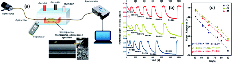 |
| | Fig. 18 (a) Schematic diagram of the gas sensing transmittance setup on the basis of an optical fiber coated with thin layers of anionic MoS2 and Au. The inset image shows the cross-sectional FE-SEM images of the anionic 2H–MoS2/Au coated optical fibre. (b) Dynamic and (c) sensitivity responses of the optical fiber sensors modified with different samples. Reprinted with permission from ref. 39. Copyright 2020, ACS Publishing. | |
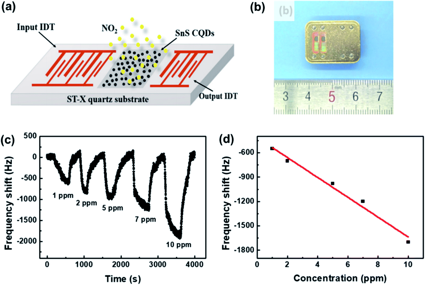
3.7 SAW gas sensors
The SAW sensor is based on the microelectromechanical system (MEMS), which converts an input electrical signal into a SAW, i.e., a mechanical wave.139Fig. 19 shows a typical SAW gas sensor structure, whose SAW delay line between the input and output interdigital-transducer (IDT) is covered by a thin membrane that can selectively adsorb the gas to be detected. Any change in phase, frequency, amplitude, or time-delay induced by gas adsorption or desorption of the membrane, might further affect the wave. Then it is converted into an electrical signal and received by the output end. In particular, the phase velocities can be detected with high accuracy. In this case, SnS colloidal quantum dots (CQDs) were used as the sensing layer and fabricated on the ST-cut quartz substrate.140 The sensor exhibited high selectivity and efficiency for the detection of NO2 gas with low concentration at room temperature. Moreover, this is an efficient approach to diagnose diseases from exhaled breath by coating SAW sensors with various polymers to identify specific breath biomarkers.
 |
| | Fig. 19 (a) The schematic and (b) a photograph of the SAW sensor based on SnS CQDs. (c) The response curves of the SAW sensor to different NO2 concentrations. (d) The dependence of the response on NO2 concentration. Reprinted with permission from ref. 140. Copyright 2019, Elsevier. | |
4. Metal sulfide-based devices for gas sensing applications
4.1 VOCs
VOCs primarily come from the exhaust gases generated by transportation, fuel combustion, and come from cooking, furniture, decorative materials, or much simpler breathing.141 Since the concentration of VOCs an indoor ambient environment is much higher than that outdoors (up to 10 times), the level of VOCs is used as one of the indicators for evaluating the air quality in indoor ambient.98 When people are exposed to a certain concentration of VOCs, they face a higher risk of suffering from headaches, nausea, and even organ damage. From a medical perspective, exhaled breath contains VOCs of alcohols, hydrocarbons, ketones, aldehydes, esters, nitriles, and aromatic compounds,142,143 which can be used as biomarkers of the diagnosis of diseases according to Fig. 1. The gas-sensing performance of metal sulfide-based devices towards different VOCs is summarised in Tables 4–6.
Table 4 Literature study on the gas-sensing performance of metal sulfide-based VOC gas sensorsa
| Material |
Structure |
Synthesis method |
Analyte |
Concentration (ppm) |
Response (%) |
LOD (ppm) |
τ
s/τr |
OT (°C) |
Ref. |
|
* means the response% is recalculated as (Xgas − X0)/X0 = ΔX/X0 in this review. In the original reference, the response (%) is defined as Xgas/Xair.
|
| SnS |
NFKs |
Solid state reaction |
Acetone |
20 |
1000 |
— |
3 s/14 s |
100 |
34
|
| ZnS |
NWs |
Thermal evaporation |
Acetone |
100 |
2120 |
0.5 |
10 s/7 s |
320 |
103
|
| MoS2 |
Nanofilm |
ME |
Acetone |
5000 |
∼1.2 |
500 |
— |
RT |
38
|
| SnS2 |
NRs |
Precipitation in aqueous solution |
Acetone |
10 |
∼2500 (dry) |
1 |
— |
300 |
147
|
| ∼210 (17% RH) |
| Pd–TiO2/MoS2 |
Nanocomposites |
Hydrothermal method |
Benzene |
50 |
64 |
0.1 |
13 s/10 s |
RT |
153
|
| ZnO/MoS2 |
p–n junction |
Screen printing |
Benzene |
20 |
30 |
0.1 |
8 s/6 s |
RT |
154
|
| Co-MPP-functionalized MoS2 |
Nanocomposites |
Solvent mixing |
Benzene |
10 |
22 |
— |
∼500 s/∼100 s |
RT |
155
|
| PbS |
NSs |
Chemical reaction |
Methane |
10000 |
∼10 |
— |
— |
RT |
159
|
| Au NPs/PbS |
Nanocomposites |
Chemical reaction |
Methane |
30000 |
30 |
— |
180 s/70 s |
RT |
160
|
| Ag NPs/PbS |
Nanocomposites |
Chemical reaction |
Methane |
80000 |
35 |
— |
60 s/150 s |
RT |
161
|
| PbS NCs/rGO |
Nanocomposites |
Chemical reaction & hydrothermal method |
Methane |
10000 |
45 |
— |
90 s/65 s |
RT |
162
|
| ZnS:Mn2+ (optical) |
QDs |
Chemical precipitation |
Methane |
100 |
∼50* |
— |
— |
RT |
164
|
| SnO2/MoS2 |
Nanocomposites |
Electrospinning and hydrothermal method |
Methane |
100 |
101.4* |
— |
150 s/20 s |
180 |
163
|
| ZnS |
0D nanosphere |
Hydrothermal method |
Formaldehyde |
50 |
9440* |
— |
11 s/8 s |
295 |
165
|
| rGO/MoS2 |
Hybrid films |
Layer-by-layer (LBL) self-assembly |
Formaldehyde |
10 |
2.8 |
— |
— |
RT |
166
|
| In2O3/MoS2 |
Nanocubes/nanofilm |
LBL self-assembly |
Formaldehyde |
50 |
75.2 |
0.2 |
14 s/22 s |
RT |
167
|
| In2O3/WS2 |
Nanocomposites |
LBL self-assembly |
Formaldehyde |
5 |
7.5 |
— |
98 s/137 s |
RT |
168
|
| Ni-doped In2O3/WS2 |
Nanocomposites |
LBL self-assembly |
Formaldehyde |
20 |
32 |
0.015 |
76 s/123 s |
RT |
4.1.1 Acetone.
Acetone is one of the common metabolites of the human body and is ordinarily present in the breath, blood, and urine. Increased acetone in the breath can be found in untreated patients with diabetes mellitus.144,145 Typically, the acetone concentration for diabetic patients is higher than 1.71 parts per million by volume (ppmv), whereas that for healthy people ranges from 0.3 to 0.9 ppmv.146 The detection and analysis of acetone in the breath can be a potential method for the diagnosis of diabetes. Besides, acetone may also be associated with lung cancer.142 To achieve high sensitivity, various shapes of metal sulfides were used. The SnS NFK-based gas sensor showed excellent stability and reproducibility at 100 °C for the detection of acetone from 5 to 50 ppm and a rapid response of 3 s.34 Wang et al.103 fabricated a single-crystal ZnS NW-based gas sensor through the thermal-evaporation-growth method, which showed high sensing selectivity towards acetone and ethanol. Giberti et al.147 obtained SnS2 NRs as a precipitate in aqueous solution and deposited them as functional materials on an alumina substrate for acetone, acetaldehyde, and H2S gas sensing. The sensor showed excellent selectivity to acetone at 1 ppm under both dry and wet conditions at an OT of 300 °C. To decrease the OT, SnS2/SnO2 heterojunctions were employed for the detection of acetone, and they showed a response% of 107% and fast recovery (80 s) at 80 °C.148 However, the LOD could not meet the limit of acetone concentration in the exhaled breath (0.9 ppm), which shows that the LOD of metal sulfide-based gas sensors needs to be improved further.
4.1.2 Benzene.
Benzene gas is volatile and highly toxic; even a small amount of benzene can cause vital harm to our body.149 The maximum permitted exposure limit in the atmosphere regulated by the World Health Organization (WHO) is 5 ppb (16.25 μg m−3).150 However, benzene is commonly used as a solvent in petrochemical and pharmaceutical goods, which has terrible carcinogenic effects on the people working there. It is necessary to detect-trace benzene in the environment, which has led to the development of inexpensive sensors for benzene detection. The conventional methods are based on cataluminescence, chromatography, and spectroscopy.149,151,152 Recently, semiconductor sensors were explored. For metal sulfide-based devices, Zhang et al.153 synthesized and used Pd-decorated TiO2/MoS2 ternary nanocomposites in the benzene sensor. Compared to pristine MoS2 and TiO2 sensors, this sensor has a higher response% of 64% for 50 ppm benzene, wider linearity ranging from 0.1 to 100 ppm, shorter response and recovery times (13 s/10 s), and better selectivity and stability. Moreover, this group employed WS2 NFWs/ZnO hollow spheres to detect benzene, which showed a faster response and recovery time of 8 s/6 s at room temperature.154 To extend the application area, Baek et al.155 demonstrated a flexible and transparent benzene sensor using cobalt-metalloporphyrin (Co-MPP)-functionalized few-layer MoS2 as the sensing material. The device has a higher response% of over 250% compared to pristine MoS2 and a low LOD of 10 ppm at room temperature.
4.1.3 Methane.
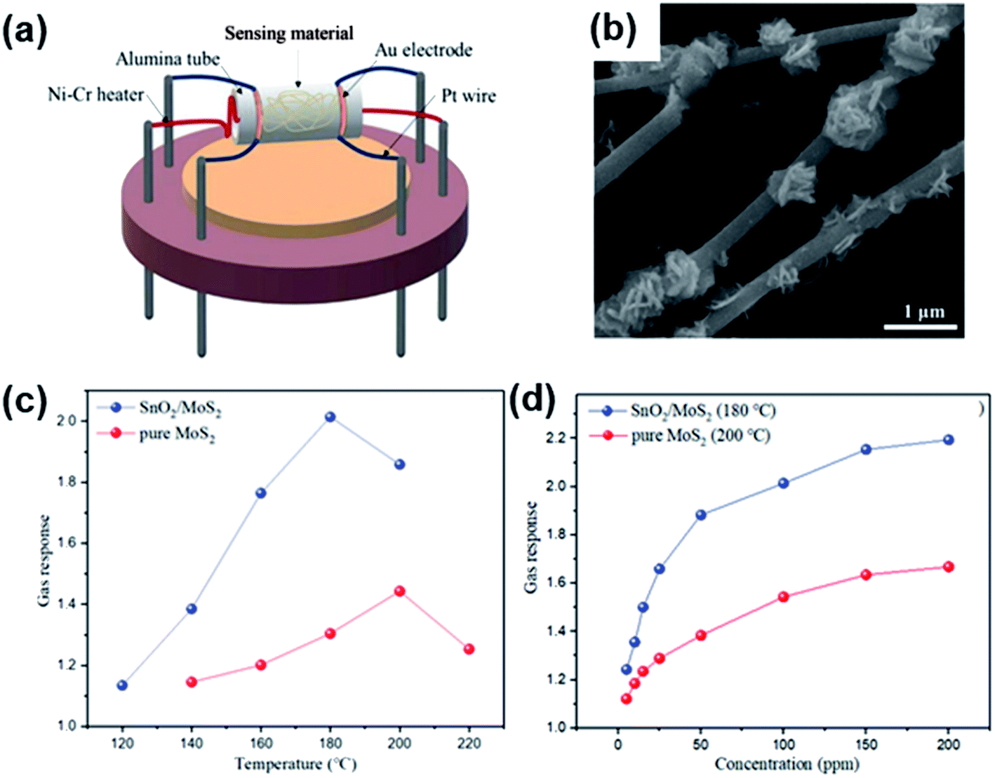
Methane (CH4) is widely present in industrial and residential areas and emitted into the atmosphere from natural wetlands, rice paddies, domestic ruminants, landfills, and biomass burning.156 It is a potent greenhouse gas, whose explosive limit concentration was reported to be more than 4.7% mixed with air.157 Traditionally, exhaled air from normal human breath doesn't have methane, except in people who are overweight and people who have irritable bowel syndrome, inflammatory bowel diseases, or anorexia.158 Taking advantage of the nanostructures, metal sulfide nanocrystals (NCs) and quantum dots (QDs) have been used in CH4 sensors. Sheikhi et al. proposed a series of PbS-based chemiresistor sensors for the detection of CH4, including intrinsic PbS NCs,159 Au nanoparticle (NP) decorated PbS,160 Ag NP decorated PbS,161 and PbS NCs/rGO hybrids.162 The PbS NCs/rGO nanocomposite sensor has shown a good response% (45%) at the lower explosive limit of CH4 with fast response and recovery time (90 s/65 s). Wang et al. employed hierarchical nanocomposites of MoS2 NFWs anchored on SnO2 nanofibers for CH4 sensing. As shown in Fig. 20, this n–n junction-based sensor showed a high response% of 101.4% toward 100 ppm CH4 at 180 °C.163 With respect to optical gas sensors, Sergeev et al.164 synthesized manganese-doped zinc sulfide (ZnS:Mn2+) QDs and found that the ZnS:Mn2+ emission spectrum is changed significantly under exposure to CH4 in the concentration range from 100 ppm to 2000 ppm. QDs in this luminescent sensor act as adsorption centres for achieving higher light transmittance and further improving the signal stability in the visible region. The response refers to the photoinduced electron transfer from QDs to CH4, which induces QD luminescence quenching and a decrease in the luminescence lifetime.
 |
| | Fig. 20 (a) Schematic structure of a SnO2/MoS2 gas sensor. (b) SEM results of SnO2/MoS2 samples. (c) Gas response of sensor devices to 100 ppm CH4 under different operating temperatures. (d) Gas response of two sensors to CH4 with various concentrations. Reprinted with permission from ref. 163. Copyright 2019, Elsevier. | |
4.1.4 Formaldehyde.
Formaldehyde (HCHO) is a colorless toxic gas with a pungent smell and can cause serious harm to the central nervous system and immune system of human beings. Because formaldehyde is a chemical used in the production of solvents, adhesives, and bonding agents, it is usually released from pressed-wood products, wallpapers, paints, and foam insulation in homes, offices, and the urban environment. According to the Occupational Safety and Health Standards, the time-weighted average limit of formaldehyde is 0.75 ppm, the short-term exposure limit is 2 ppm and the immediately dangerous to life or health limit is 20 ppm.169 In the view of healthcare, HCHO could act as a biomarker of multiple diseases, especially lung cancer.150
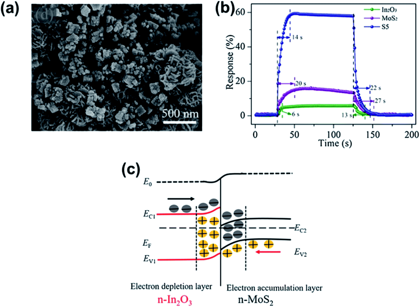
Hussain et al.165 successfully prepared 0D ZnS nanospheres via a low-temperature hydrothermal synthesis method. The gas sensor showed a high response% of 9540% and high selectivity towards formaldehyde compared to other gases (ethanol, ammonia, acetone, methanol, and NO2) at an OT of 295 °C. The enhanced gas-sensing performances can be attributed to the presence of more active sites because of the large exposed surface area and small size of ZnS nanospheres. Li et al.166 fabricated gas sensors based on rGO/MoS2 hybrid films, which yielded flexible devices for formaldehyde detection at room temperature. The mechanisms for enhanced sensing performance of the rGO/MoS2 hybrid films could be summarized as follows: in the hybrid film, MoS2 nanosheets acted as the formaldehyde adsorbent and electron acceptor, mediating a two-stage electron transfer from formaldehyde and finally to rGO, which served as a conducting network and exhibited a p-type response. As shown in Fig. 21, Zhang et al. demonstrated some room temperature formaldehyde sensors based on a LBL self-assembled In2O3 nanocubes/flower-like MoS2 nanofilm,167 and Ni-doped In2O3/WS2 nanocomposite.168 They exhibited a low LOD of 15 ppb, good selectivity, repeatability, fast detection rate, and a fair logarithmic function toward formaldehyde concentration. The dramatically enhanced sensing performance of the Ni–In2O3/WS2 sensor can be attributed to the Ni ion doping and synergistic interfacial incorporation of the In2O3/WS2 heterojunction.
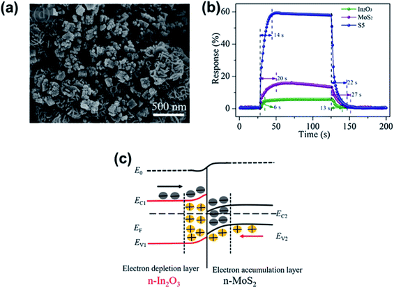 |
| | Fig. 21 (a) SEM images of In2O3 nanocubes/flower-like MoS2 hybrids. (b) The response and recovery characteristics of In2O3, MoS2 and In2O3/MoS2 (S5) film sensors exposed to 50 ppm HCHO gas. (c) The energy band diagram for the n–n junction of the In2O3/MoS2 film. Reprinted with permission from ref. 167. Copyright 2018, Elsevier. | |
4.1.5 Ethanol.
Volatile alcohols such as ethanol are often found in the chemical, medical, pharmaceutical, and food industries. They can induce nasal and mucous membrane inflammation, respiration disruption, eyesight disturbance, nerve disease, lung irritation, and even death after long-term exposure to even a low alcohol vapour concentration. On the other hand, because ethanol is a kind of flammable gas, it is essential to monitor its real-time concentration in workplaces. Moreover, ethanol is one of the typical biomarkers for lung cancer. Thus it requires developing a high-performance gas sensor for the detection of low concentration ethanol.
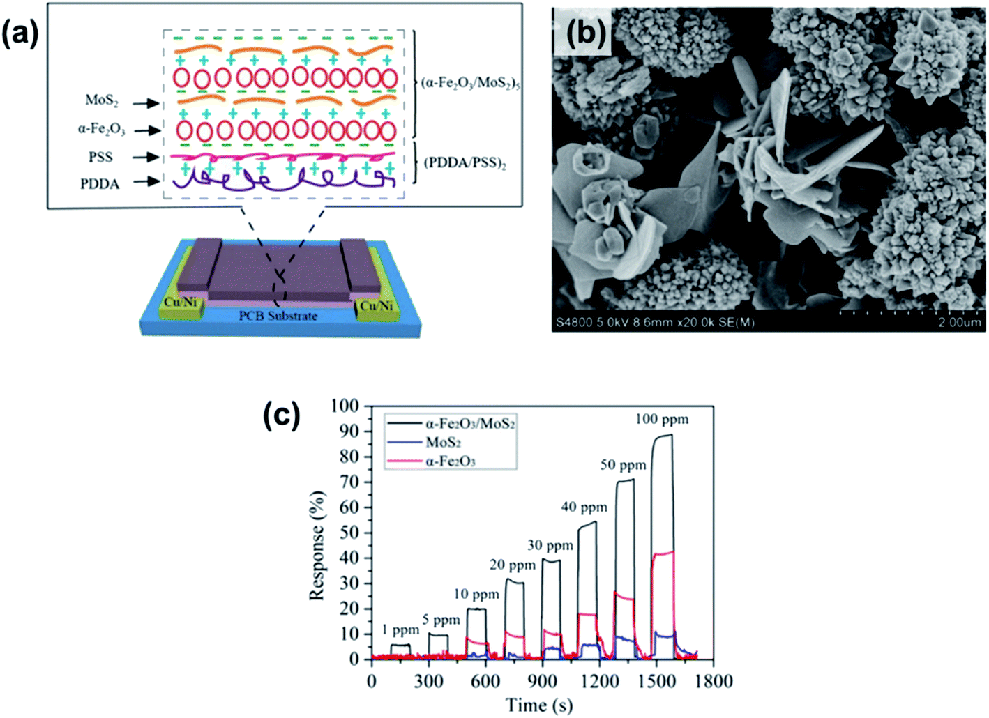
Many pristine metal sulfides, such as SnS NFKs,34 CdS thin films,171 hollow sphere CuS,172 and β-In2S3 thin films,173 were proposed for the detection of ethanol. At an OT of 300 °C, the CdS films show a high response% of 6300% and strong selectivity to alcohols in mixtures where aldehydes and other interferents are present. Their response and recovery time are speedy; however, their OTs are higher than 200 °C. Therefore, heterostructures of metal sulfides with metal oxides are introduced to enhance the sensing capability for alcohol detection. Both metal oxides and metal sulfide would have the same Fermi energy level at the interface, which results in a staggered band offset and a built-in internal electric field. When using the heterogeneous structure in a sensor, the electron generated from the adsorption reaction can easily move across the interface and transfer to the conductive band. In the context of metal sulfide/metal oxide heterostructures prepared through hydrothermal methods, MoS2/SnO2,119 MoS2/ZnO,174 and MoS2/TiO2 (ref. 175) are three typical heterostructures. Among them, the MoS2/SnO2 sensor showed an ultra-high response% of 11900% toward 200 ppm ethanol. All of them have fast response and recovery time (∼20 s),; however, their OTs are higher than 150 °C. Thus a room-temperature ethanol sensor based on n-type α-Fe2O3 hollow microspheres on MoS2 NSs prepared by the LBL self-assembly method was proposed and is shown in Fig. 22.170 The α-Fe2O3/MoS2 sensor has a low LOD of 1 ppm with high response, as well as a short response/recovery time of 6 s/5 s, which is shorter than those of α-Fe2O3 or MoS2 devices. The enhancement performance of the α-Fe2O3/MoS2 was attributed to the increased active sites for gas molecule adsorption, defects, or oxygen vacancies, when α-Fe2O3 into MoS2 nanosheets. Besides, Li et al.130 modified CdS NWs with CeO2 NPs and found that the 5 wt% CeO2/CdS n–n heterostructures exhibited a much higher response% toward 100 ppm ethanol (∼5100%), which was 2.6 times larger than that of pure CdS. The gas sensing properties of different metal sulfide-based ethanol sensors are listed in Table 5.
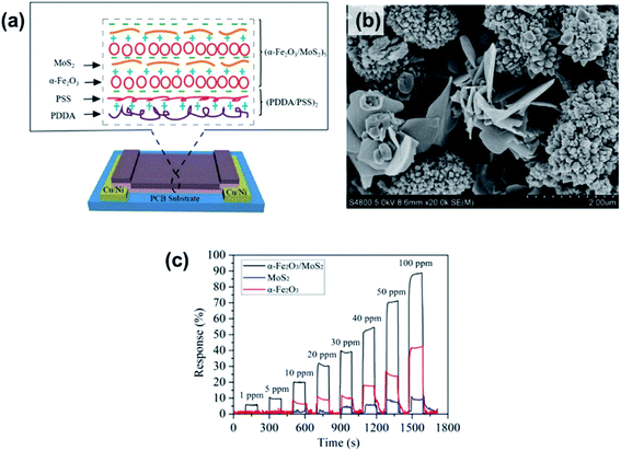 |
| | Fig. 22 (a) Schematic of an α-Fe2O3/MoS2 gas sensor. (b) SEM image of the α-Fe2O3/MoS2 nanocomposite. (c) Time-dependent response of the α-Fe2O3/MoS2, α-Fe2O3, and MoS2 film sensors towards various ethanol gas concentrations. Reprinted with permission from ref. 170. Copyright 2018, Elsevier. | |
Table 5 Gas sensing properties of metal sulfide-based sensors for ethanol
| Material |
Structure |
Synthesis method |
Concentration |
Response (%) |
LOD (ppm) |
τ
s/τr |
OT (°C) |
Ref. |
| SnS |
NFKs |
Solid state reaction |
10 ppm |
130 |
— |
2 s/9 s |
200 |
34
|
| CdS |
Thin film |
Screen printing |
5 ppm |
6300 |
— |
∼400 s/∼400 s |
300 |
171
|
| CuS |
Hollow spheres |
Surfactant micelle-template inducing reaction |
800 ppm |
1300* |
— |
15 s/15 s |
210 |
172
|
| β-In2S3 |
Thin film |
Spray pyrolysis |
500 ppm |
70* |
— |
150 s/155 s |
350 |
173
|
| MoS2/SnO2 |
Nanocomposites |
Hydrothermal method |
200 ppm |
11900* |
— |
∼20 s/∼20 s |
280 |
119
|
| MoS2/ZnO |
Nanocomposites |
Hydrothermal method |
50 ppm |
4180* |
— |
∼20 s/∼20 s |
260 |
174
|
| 0D-MoS2/TiO2 |
p–n heterojunction |
Hydrothermal method |
100 ppm |
1320* |
— |
∼20 s/∼15 s |
150 |
175
|
| α-Fe2O3/MoS2 |
Nanocomposite |
LBL self-assembly |
100 ppm |
88.9 |
1 |
6 s/5 s |
RT |
170
|
| CdS/CeO2 |
NWs |
Solvothermal method |
100 ppm |
5100* |
— |
12 s/3 s |
161 |
130
|
Table 6 Gas sensing properties of metal sulfide-based sensors for LPG gases
| Material |
Synthesis method |
Concentration (ppm) |
Response (%) |
LOD (ppm) |
τ
s/τr |
OT (°C) |
Ref. |
|
p-Polyaniline/n-PbS |
Chemical bath deposition and electrodeposition |
780 |
70 |
— |
125 s/200 s |
RT |
176
|
| n-Bi2S3/p-CuSCN |
Chemical deposition |
1370 |
70 |
— |
180 s/142 s |
RT |
178
|
| n-Bi2S3/p-PbS |
Successive ionic layer adsorption and reaction (SILAR) |
1000 |
72 |
— |
300 s/170 s |
RT |
177
|
| n-CdO/p-PbS |
SILAR |
1176 |
51.1 |
— |
150 s/134 s |
RT |
179
|
| n-CdS/p-PbS |
SILAR |
1200 |
60 |
— |
120 s/105 s |
RT |
180
|
| CdS/SnO2 |
Screen printing |
5000 |
7000 |
— |
40 s/110 s |
200 |
181
|
| n-CdS/p-polyaniline |
Electrodeposition |
1040 |
80 |
— |
105 s/165 s |
RT |
182
|
| ZnS/polyacrylamide |
Thermal frontal polymerization |
5 vol% |
62 |
— |
180 s/480 s |
RT |
183
|
| PbS/polyacrylamide |
285 |
— |
120 s/300 s |
4.1.6 Liquefied petroleum gas (LPG).
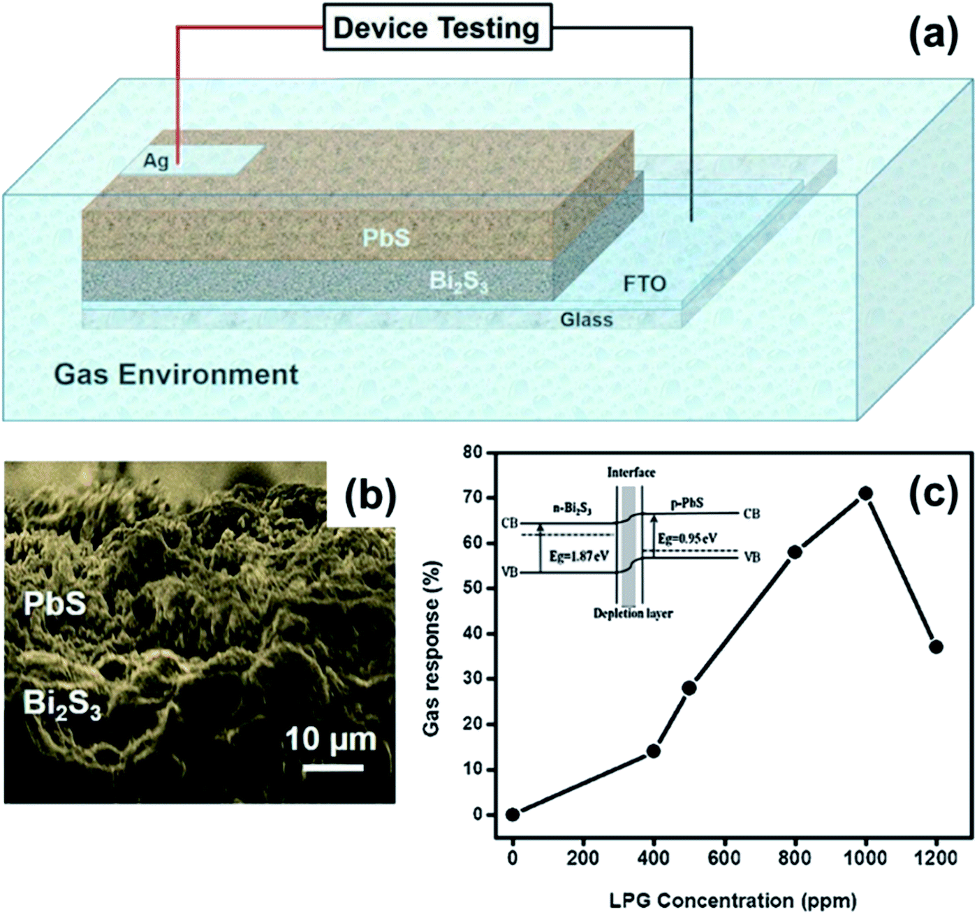
LPG is primarily composed of propane or butane and is widely used as fuels in vehicles, cooking, and heating appliances. LPG is potentially dangerous because it may cause suffocation or even an explosion when it leaks accidentally. Various types of heterojunctions were found to achieve a high gas response due to their nm-level crystalline size and the specific surface area. Patil et al.176 reported an LPG sensor based on p-polyaniline/n-PbS heterojunctions, which showed a maximum response up to 70% at 0.06 vol% LPG at room temperature. As shown in Fig. 23, Ladhe et al. successfully proposed an n-Bi2S3/p-PbS177 heterojunction for room temperature LPG sensors, which showed ∼70% response towards 1000 ppm LPG with fast response and recovery time. Moreover, n-Bi2S3/p-CuSCN,178 n-CdO/p-PbS,179 n-CdS/p-PbS,180 CdS/SnO2,181 n-CdS/p-polyaniline,182 and ZnS/polyacrylamide183 demonstrated potential application in LPG detection. It is found that the alignment of energy bands at the interface of these heterojunctions shows the importance of gas sensing owing to the changes in barrier height of junction after exposure to the LPG gas environment.
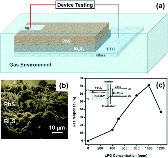 |
| | Fig. 23 (a) Schematic representation of the n-Bi2S3/p-PbS heterojunction device. (b) SEM image of the n-Bi2S3/p-PbS heterojunction. (c) The plot of variation in gas response (%) vs. LPG concentration (ppm) of the n-Bi2S3/p-PbS heterojunction. The inset shows the band diagram of the n-Bi2S3/p-PbS heterojunction. Reprinted with permission from ref. 177. Copyright 2017, Elsevier. | |
4.2 Inorganic gases
Inorganic gases are essential for environment detection and as biomarkers in medical monitoring. The primary gases of interest are NH3, NO, NO2, CO2, O2, H2S, SO2, H2, and humidity. This section will discuss metal sulfide-based devices for the detection of various inorganic gases.
4.2.1 NH3.
High concentrations of NH3 could severely irritate the nose and throat of human beings and 1000 ppm vapours can cause pulmonary edema. Low concentrations of NH3 also could hurt the skin, eyes, and respiratory system after prolonged exposure.184 Thus, the maximum permissible limit of NH3 is 20 ppm for 8 hours.7 Besides, NH3 is present in the breath samples of healthy people and patients with renal disease. According to reports, the exhaled NH3 concentration for healthy people ranges from 0.43 to 1.80 ppm, while that for end-stage renal disease patients ranges from 0.82 to 14.70 ppm.185 Liu et al.186 first presented high-performance room temperature chemical sensors based on Schottky-contact CVD MoS2. The devices showed a response% of 20% toward 20 ppb of NO2 and 40% toward 1 ppm of NH3. The WS2 NFK-based gas sensor showed p-type sensing behaviour and excellent response% of ∼1500% towards 5 ppm NH3 at room temperature.187 Xiong et al.188 fabricated an NH3 sensor based on SnS2 NFWs via a solvothermal process. The sensors exhibited a high response% of 640%, short response/recovery time of 40.6 s/624 s and a low LOD of 0.5 ppm NH3. Late et al.83 compared and analyzed the gas sensing behaviours of single-layer (SL) and multilayer (ML) MoS2 transistor-based sensors towards NO2, NH3, and humidity, see Fig. 17. They found that the SL-MoS2 sensor was unstable; the 5L-MoS2 sensor showed a stronger response to a bias voltage, and the gas sensing response was enhanced after applying gate voltage. Moreover, phototransistor gas sensors of WS2 (ref. 189) and ReS2 (ref. 190) were employed for NH3 gas detection, whose response and recovery times were fast.
Benefitting from the interfacial Coulomb scattering and strong charge transfer, heterojunction-based devices have been used as NH3 gas sensors. Zhang et al.191 prepared MoS2/ZnO nanocomposites comprising ZnO NRs and MoS2 NSs, which could detect down to 12 ppb NH3. Response/recovery times of 10 s/11 s were observed towards 50 ppm NH3 at room temperature. The first MoS2/Co3O4 nanocomposite NH3 sensor was demonstrated by Sun et al., which showed a high response of 10.3% towards 100 ppb NH3 with a response and recovery time of 98 s/100 s at room temperature, see Fig. 24a.192 Moreover, an ultrahigh performance NH3 sensor based on a nanoporous MoS2/VS2 heteroarchitecture was successfully fabricated. As shown in Fig. 24b, the gas-sensing performance investigated using a quartz crystal microbalance (QCM) reveals that MoS2/VS2 exhibits a high adsorption uptake of Δf = 344.5 Hz toward 5 ppm NH3, which is much better than that of previously reported QCM NH3 sensors.193 Other p–n heterojunction gas sensors, for instance, 2D WS2 NSs decorated with TiO2 QDs, were proved to have a high response to NH3 gas at room temperature.194 Xu et al.117 and Leonardi et al.195 synthesized SnO2–SnS2 p–n heterojunctions by the oxidation of SnS2 at high annealing temperature. The devices exhibited fast response time (11 s) at room temperature, much faster than that of other NH3 sensors. For other heterojunction gas sensors, Pr-SnS2/ZnS,129 PbS/TiO2,196 and PbS/NaS2 (ref. 197) were proposed as sensing materials for NH3 detection. Pr-SnS2/ZnS showed a high response% of 1303% and fast response/recovery time of 6 s/13 s towards 50 ppm NH3 at an OT of 160 °C, and PbS/NaS2 had a high response% of 30000% when exposed to 8.08% NH3 at room temperature. The gas-sensing performances of various metal sulfide-based NH3 gas sensors are listed in Table 7. It was found that the sensor based on metal oxide/metal sulfide heterojunctions exhibits higher response% and lower LOD.
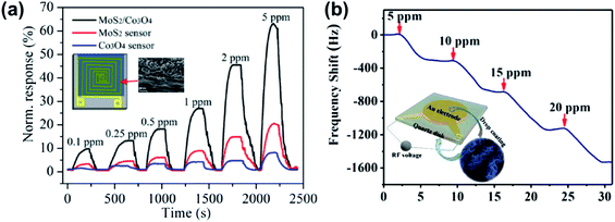 |
| | Fig. 24 (a) Normalized response of the MoS2/Co3O4 MoS2, and Co3O4 film sensors toward various NH3 concentrations (inset: the schematic of the MoS2/Co3O4 gas sensor and SEM image of MoS2/Co3O4). Reprinted with permission from ref. 192. Copyright 2017, ACS Publishing. (b) The mass-normalized time-dependent frequency shifts of NH3 adsorption on the MoS2/VS2 heterostructure at 40 °C (inset: illustration of the QCM experimental sensor prepared via drop-coating of the MoS2/VS2 heterostructure onto the Au electrode). Reprinted with permission from ref. 193. Copyright 2019, Wiley-VCH Verlag GmbH & Co. KGaA, Weinheim. | |
Table 7 Literature study on the gas-sensing performance of metal sulfide-based NH3 gas sensors
| Material |
Structure |
Synthesis method |
Concentration |
Response (%) |
LOD (ppm) |
τ
s/τr |
OT (°C) |
Ref. |
| MoS2 (green illumination) |
Transistor |
ME |
1000 ppm |
86 |
— |
∼800 s/1500 s |
RT |
83
|
| WS2 |
NFKs |
Ball milling |
5 ppm |
∼1400* |
— |
∼120 s/∼150 s |
RT |
187
|
| Phototransistor |
ME |
— |
— |
— |
2.6 s/56 s |
RT |
189
|
| ReS2 |
Phototransistor |
ME |
— |
— |
— |
∼70 ms/∼70 ms |
RT |
190
|
| SnS2 |
2D SnS2 with sulfur vacancies |
Chemical exfoliation |
500 ppm |
420 |
— |
16 s/450 s |
RT |
109
|
| NFWs |
Solvothermal method |
100 ppm |
640* |
0.5 |
40.6 s/624 s |
200 |
188
|
| NFWs |
Hydrothermal method |
5 ppm |
21.6 |
— |
40–50 s/100–120 s |
RT |
198
|
| Graphene/MoS2 |
Heterostructure |
ME-MoS2 |
100 ppm |
6 |
— |
NA/30 min |
150 |
199
|
| CVD-graphene |
| MoS2/ZnO |
Nanocomposites |
LBL self-assembly |
50 ppm |
46.2 |
0.012 |
10 s/11 s |
RT |
191
|
| MoS2/CuO |
Nanoworms |
Sputtering |
100 ppm |
47 |
5 |
17 s/26 s |
RT |
200
|
| MoS2/Co3O4 |
Nanocomposites |
LBL self-assembly |
0.1 ppm |
10.3 |
0.1 |
98 s/100 s |
RT |
192
|
| MoS2/VS2 |
Heterostructure, QCM |
Hydrothermal method |
5 ppm |
Δf = 344.5 Hz |
— |
— |
40 |
193
|
| WS2/TiO2 |
Nanocomposites |
Mixture solution |
500 ppm |
56.69 |
20 |
200 s/174.43 ± 13.75 s |
RT |
194
|
| SnS2/SnO2 |
NFKs |
Annealing |
50 ppm |
40* |
— |
∼60 s/∼300 s |
130 |
195
|
| Hybrids |
Oxidation |
10 ppm |
16* |
— |
11 s/NA |
RT |
117
|
| Pr-SnS2/ZnS |
NFWs |
Hydrothermal method |
50 ppm |
1303* |
— |
6 s/13 s |
160 |
129
|
| PbS QDs/TiO2 |
NTs |
SILAR |
100 ppm |
1649* |
2 |
∼10 s/∼10 s |
RT |
196
|
| PbS/NaS2 |
NPs |
— |
8.08% |
30000* |
— |
46 s/67 s |
RT |
197
|
4.2.2 NO2 and NO.
NO2 is one of the most abundant air pollutants and is primarily emitted by fossil fuel burning, road traffic, indoor combustion,201 and biomass burning.202 It induces acid rain and photochemical smog. High concentrations of NO2 can irritate the human respiratory system. Long exposures to low NO2 concentrations also cause the development of asthma and respiratory symptoms. NO in exhaled breath is associated with inflammation of the air path, such as asthma and bronchiectasis. It is a typical biomarker for chronic obstructive pulmonary disease and nasal polyposis.203 The recommended concentration of NO for healthy people is below 25 ppb; when it is higher than 50 ppb, it is perhaps a sign of airway inflammation.204 Notably, NO is easily oxidized to NO2, indicating that it is challenging to detect NO directly using semiconductor gas sensors. Sometimes, the concentration of NO is usually reflected indirectly by detecting NO2. Li et al.82 proposed a MoS2 FET NO sensor and compared and analyzed the sensors with monolayer, bilayer, trilayer, and quadrilayer MoS2. The response of the monolayer sensor is rapid and dramatic but unstable. In contrast, the multilayer sensors are stable and show sensitive responses down to a LOD of 0.8 ppm NO. TaS2 NSs exfoliated by electrochemical lithium intercalation have been employed for the detection of NO and showed a high response% of 6000% towards 500 ppm NO and exhibited a sub-ppm LOD.60 A TaS3 nanofibre NO gas sensor exhibited a high sensitivity of 4.48° μM−1 and a low LOD of 0.48 ppb, well under the allowed value set by the WHO, see Fig. 25.65 The different types of NO and NO2 gas sensors based on metal sulfides are summarised in Table 8.
 |
| | Fig. 25 (a) Impedance responses of the TaS3 sensor fabricated in polyester, parafilm, and paper under different NO concentrations from 0 to 16.2 μM. (b) Calibration curves of the TaS3 gas sensor fabricated in polyester and paper at different NO concentrations. (c) Selectivity study comparison of the TaS3 gas sensor fabricated in all configurations (paper, parafilm, and polyester). The inset image shows the schematic representation of various TaS3 nanofiber-based devices. Reprinted with permission from ref. 65. Copyright 2018, ACS Publishing. | |
Table 8 Literature study on the NOx sensing performance of metal sulfide-based devices
| Material |
Structure |
Synthesis method |
Analyte |
Concentration (ppm) |
Response (%) |
LOD |
τ
s/τr |
OT (°C) |
Ref. |
| SnS |
Thin crystal |
Solvothermal method |
NO2 |
0.1 |
20 |
— |
NA/5 s |
RT |
33
|
| CdS |
Thin film |
Chemical route |
NO2 |
20 |
17300 |
— |
331 s/207 s |
70 |
205
|
| Thin film |
Chemical bath deposition |
NO2 |
200 |
61 |
— |
50 s/NA |
RT |
206
|
| PbS |
Thin film |
Chemical bath deposition |
NO2 |
100 |
74 |
— |
20 s/36 s |
38 |
100
|
| Thin film |
SILAR |
NO2 |
50 |
35 |
— |
6 s/97 s |
150 |
207
|
| TaS2 |
NSs |
Electrochemical lithium-intercalation |
NO |
5 |
60 |
— |
— |
RT |
60
|
| TaS3 |
Nanofibres |
Vapour-phase growth |
NO |
— |
Sensitivity 4.48° μM−1 |
0.48 ppb |
— |
RT |
65
|
| MoS2 |
Transistor |
ME |
NO |
2 |
80 |
0.8 ppm |
— |
RT |
82
|
| Transistor |
ME |
NO2 |
1000 |
1372 |
— |
∼800 s/1500 s |
RT (green light) |
83
|
| NFKs |
LPE |
NO2 |
1 |
15 (p-type) |
20 ppb |
11 s/22 s |
200 |
29
|
| 480 (n-type) |
41 s/39 s |
| WS2 |
NSs |
Hydrothermal method & calcination |
NO2 |
0.1 |
9.3 |
100 ppb |
5 min/25 min |
RT |
208
|
| SnS2 |
2D |
Ball milling |
NO2 |
10 |
2000 |
— |
6/40 s |
250 |
209
|
| 2D flakes |
Solvothermal method |
NO2 |
10 |
3533* |
— |
∼170 s/∼140 s |
120 |
210
|
| NbS2 |
NSs |
CVD |
NO2 |
10 |
2832 |
241.02 ppb |
3000 s/9000 s |
RT |
59
|
| Ag NWs–WS2 |
NSs |
ALD |
NO2 |
500 |
667 |
— |
5 min/10 min |
RT |
211
|
| Al/MoS2 |
Schottky contact |
CVD |
NO2 |
10 |
60 |
— |
∼5 min/∼20 min |
RT |
111
|
| Au/Gr–MoS2–Gr/Au |
Schottky contact |
CVD |
NO2 |
0.15 |
500* |
0.1 ppb |
∼1000 s/∼700 s |
RT (red light) |
114
|
| Gr–MoS2 |
Schottky contact |
ME |
NO2 |
1 |
160000 |
— |
— |
RT |
212
|
| MoS2/SnO2 |
Heterostructures |
Chemical methods |
NO2 |
5 |
1770* |
— |
74 s/NA |
RT |
121
|
| MoS2/ZnO |
NWs |
Hydrothermal method & CVD |
NO2 |
50 |
31.2 |
0.2 ppm |
60 min/65 min |
200 |
213
|
| rGO–MoS2–CdS |
Nanocomposite |
Hydrothermal method |
NO2 |
0.2 |
27.4 |
— |
25 s/34 s |
75 |
214
|
| WS2/WO3 |
Nanocomposites |
Oxidation |
NO2 |
0.4 |
100* |
400 ppb |
— |
150 |
215
|
| WS2/ZnS |
Heterostructures |
LPE-WS2, chemical method |
NO2 |
5 |
3150* |
10 ppb |
4 s/∼400 s |
RT |
216
|
| WS2/IGZO |
Heterojunction |
CVD, sputtering |
NO2 |
5 |
6820 |
26 ppb |
— |
RT |
217
|
| 300 |
499400 |
| SnS2/SnO2 |
Nanocomposites |
Oxidation |
NO2 |
8 |
430* |
1 ppm |
159 s/297 s |
80 |
148
|
| SnS2/SiO2 |
Nanograins |
CVD |
NO2 |
10 |
701 |
408.9 ppb |
272.8 s/3800.4 s |
RT |
218
|
| SnS2/rGO |
Heterojunction |
Hydrothermal method |
NO2 |
8 |
49.8 |
8.7 ppb |
NA/76 s |
RT |
219
|
| PbS QDs/MoS2 |
Nanocomposites |
Hydrothermal method & chemical precipitation |
NO2 |
100 |
∼23 |
— |
30 s/235 s |
RT |
220
|
| ZnS/CuO |
NWs |
Thermal evaporation & solvothermal method |
NO2 |
5 |
955* |
— |
45 s/170 s |
RT (UV light) |
133
|
Wang et al.33 proposed a NO2 gas sensor using large-sized SnS thin crystals, which present a high response% of 20% towards NO2 at a 100 ppb concentration, as well as superior selectivity, low LOD (≪100 ppb), and reversibility at room temperature. Benefitting from a large excitation Bohr radius (18 nm), PbS thin films were synthesized and applied in NO2 detection, and they exhibited a response% of 35% for 50 ppm NO2 at 150 °C with a rapid response time of 6 s.207 Recently, Sonker et al.205 used a sol–gel method for fabricating CdS NPs, which can detect 20 ppm NO2 gas with a response% of 17300% at 70 °C. Donarelli et al.29 found that LPE-MoS2 NFKs after annealing in air at 150 °C and 250 °C can show a p-type and n-type conductivity, respectively. The p-type MoS2 showed 15% response towards 1 ppm with fast response/recovery time (11 s/22 s), while the n-type MoS2 exhibited a higher response% of 480% and a lower LOD of 20 ppb. Xu et al.208 synthesized ultra-thin WS2 NSs through a hydrothermal and calcination process, which showed a high response of 9.3% after exposure to 0.1 ppm NO2 gas at room temperature. Ko et al.211 proved that the WS2 gas sensor showed dramatically improved response (667%) and recovery upon NO2 exposure after functionalization with AgNWs. Another WS2/WO3-based gas sensor showed an excellent LOD of 40 ppb in dry air for NO2 at an OT of 150 °C.215 2D SnS2-based gas sensors presented a high response% of 3533% toward 10 ppm NO2 and showed highly selective and reversible NO2 sensing.210 Kim et al.59 fabricated a room temperature NO2 sensor using 2D NbS2, which showed a response% of 2832% toward 10 ppm NO2 and a low LOD of 241.02 ppb.
For metal–metal sulfide Schottky junctions, Liu et al.186 observed a considerable SB in the Ti/Au electrodes and at the CVD-MoS2 contact interface, which showed a conductance change of 2–3 orders of magnitude upon exposure to sub-ppb level concentrations of NO2 and NH3. Besides, vdW vertical Schottky junctions of graphene and semiconductors have attracted considerable attention as emerging transducers for gas sensors. Tabata et al.212 deeply analyzed the NO2 gas-sensing performance of a graphene/MoS2-based gas sensor, where the SBH was modulated by bias- and gate-voltage. The device exhibited an ultra-high response% of 160000% after 10 min exposure to NO2. To know the difference between the Schottky junction of metal–metal sulfides and graphene–metal sulfides, Pham et al.114 compared and analyzed the gas-sensing performances of CVD MoS2 with Au metal electrodes (Au–MoS2–Au), graphene electrodes (Gr–MoS2–Gr), and graphene/Au electrodes (Au/Gr–MoS2–Gr/Au). The resulting Au/Gr–MoS2–Gr/Au gas sensor under red light illumination showed a significant enhancement of the device response% toward 150 ppb of NO2 gas reaching 500% (see Fig. 26). The excellent performance could be attributed to the encapsulation of graphene electrodes with the Au layer affecting the work function of graphene, resulting in an increasing SBH. Furthermore, Au/Gr electrodes could hinder the negative effects of the modulation of the work function induced by the doped graphene with NO2 molecules.
 |
| | Fig. 26
I–V curves under red LED illumination (red line) and in the dark (black line) of (a) Au–MoS2–Au, (b) Gr–MoS2–Gr, and (c) Au/Gr–MoS2–Gr/Au devices. The insets show the corresponding schematics of the devices and expanded I–V curves in the dark. (d–f) Dependence of the normalized amplitude of the resistance change of (d) Au–MoS2–Au, (e) Gr–MoS2–Gr, and (f) Au/Gr–MoS2–Gr/Au devices on the concentration of NO2 gas. The inset image shows a temporal trace of the experimentally recorded noise of ΔR/RN2. All data were collected under a dc bias of 5 V. Reprinted with permission from ref. 114. Copyright 2019, ACS Publishing. | |
For heterojunction-based devices, MoS2/SnO2 p–n heterojunctions were constructed and used for ethanol, TMA, and NO2 gas sensing.119–121 They exhibited high sensitivity, lower OT, excellent sensing selectivity, and outstanding long-term stability. Shao et al.214 fabricated rGO–MoS2–CdS nanocomposite films via solvothermal treatment and analyzed the sensing performance. The results showed a largely enhanced sensor response of 27.4% toward 0.2 ppm NO2, approximately 7 times higher than the value for the rGO–MoS2 based gas sensor. Moreover, a SnO2–SnS2 p–n heterojunction was employed in the NO2 gas sensor.117,148
A FET gas sensor was used for NO2 gas sensing because the conductance of the channel can be modulated by applying different bias voltages on the gate electrode. Late et al.83 analyzed the NO2 sensing behaviours of the MoS2 transistor, Fig. 17. The response was enhanced after applying gate bias. Similarly, WS2 (ref. 189) and ReS2 (ref. 190) FETs were employed to detect different gases, such as O2, NH3, and NO2. As mentioned in Section 3.5, the strong electron transfer between the FET channel materials and the gas molecule could alter the carrier concentration of the channel, modulate the mobility, further affect semiconductor work function, and finally change the current of the FET.221,222 Based on this mechanism, our group analyzed a WS2/IGZO p–n junction-based gas sensor in chemiresistor and transistor mode, respectively.217 It was found that the transistor shows an ultra-high response after exposure to NO2, with a response% of 499400% for 300 ppm, which is ∼27 times higher than that in chemiresistor mode (see Fig. 27a–c). One special case reported by Tabata et al.212 is the graphene/MoS2 heterojunction (GMH) sensor. As shown in Fig. 27d–f, the device had a high response% to NO2 of 160000% at a 0 V back-gate voltage (VBG); however, when VBG = 40 V, the response% decreased to 600%. They found that the drain current was primarily determined by the SBH at the counter Schottky diode of the MoS2/Ti contact, and the NO2-induced modulation in the SBH at the GMH was not reflected in the sensor response. Last but not least, the SAW NO2 sensor uses SnS CQDs as the sensing layer and is fabricated on a quartz substrate.140 The sensor could detect a low concentration of NO2 gas at room temperature with a good efficiency and selectivity (see Fig. 19).
 |
| | Fig. 27 (a) Schematic diagram and (b) optical image of the WS2/IGZO transistor. (c) Transfer curves of the WS2/IGZO transistor under different NO2 concentrations. Reprinted with permission from ref. 217. Copyright 2019, ACS Publishing. (d) Schematic diagram and (e) optical image of the graphene/MoS2 heterojunction (GMH) device with a gas barrier layer. (f) Time-dependent sensor responses of GMH under different gate voltages (VBG = 0 and 40 V). Reprinted with permission from ref. 212. Copyright 2019, ACS Publishing. | |
4.2.3 CO2 and O2.
CO2 is the fourth most abundant component of dry air. Tests have shown that 5% CO2 is not harmful to humans if sufficient oxygen is present, but once the O2 concentration is less than 17%, even 4% CO2 can cause severe poisoning. Considering that the ambient concentration of CO2 is approximately 0.03%, the required LOD for CO2 sensors could be at the ppm-level. Because CO2 is a kind of nonpolar gas owing to its linear and symmetrical structure, the adsorption energy between CO2 and the surface of metal sulfides is low. To this end, a new optical CO2 sensor based on the colorimetric change of the pH indicator α-naphtholphthalein with the internal reference fluorescent CIS/ZnS QDs was developed.223,224 The experimental result reveals that the new optical CO2 sensor has a response% of (I100 − I0)/I0 × 100% = 1240%. Similarly, Chu et al.225 developed a CdSe/ZnS QD based optical fibre CO2 sensor, which showed a high response% of (R0 − R)/R × 100% = 84% and exhibited a uniquely linear response to CO2 concentrations in the range of 0–100%. The gas testing setup of the fibre-optic CO2 sensor is shown in Fig. 28, and this testing method can quantitively measure the CO2 concentration; however, it cannot detect changes of the fluorescence spectra in real-time.
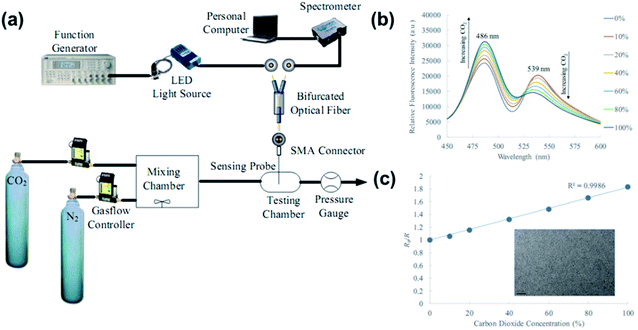 |
| | Fig. 28 (a) Experimental setup for the ratiometric optical fibre CO2 sensing. (b) Fluorescence spectra of the ratiometric optical fibre sensor under different CO2 concentrations. (c) Calibration curve of the ratiometric optical fibre CO2 sensor at 0–100% concentration. Reprinted with permission from ref. 225. Copyright 2019, SPIE publishing. | |
O2 is a major component of air and greatly affects metal corrosion protection, fuel combustion, and food storage. It is essential to monitor the O2 content in industrial production and medical care. Metal sulfide nanomaterials for O2 sensing have not been extensively studied. Kim et al.226 prepared MoS2 NP-based gas sensors through LPE methods and investigated their O2 sensing behaviour, which showed a high response% of 769% towards a 2% concentration of O2 and a low LOD at the ppb level. Li et al.227 proposed a 2D SnS2-based sensor, which provided high and reversible responses to O2 pulses in the range of 0 to 20% volume in the dark at 150 °C. They applied UV irradiation for improving the O2 sensing performance. Karami et al.228 synthesized SnS–SnO2 nanocomposites and used them as O2 gas-sensing agents, which showed a high dynamic range, high sensitivity to O2, fast response time, and low memory effect without any interference from the other gases (OT = 128 °C).
4.2.4 H2S and SO2.
Both H2S and SO2 are hazardous gases and atmospheric pollutants. H2S smells like rotten eggs and irritates people's eyes, nose, and throat. Long-term exposure to H2S above 100 ppm can cause death. In the human body, H2S is a kind of metabolic product that has an unpleasant odor and is associated with halitosis. SO2 is highly corrosive and easily oxidized to create sulfuric acid in the air. These two gases pose significant threats to the environment and human health and require accurate measurement.
PbS CQDs have been used as H2S gas sensing materials, and they exhibit a response% of 421700% towards 50 ppm H2S, which is considerably high, and a fast response/recovery time of 23 s/171 s.101 Metal oxide/metal sulfide heterojunctions, such as ZnS/ZnO132 and CuS/CuO,229 have been employed for the detection of H2S gas, see Fig. 29. Souda and Shimizu106 tested various metal monosulfide-based gas sensors (NiS, CdS, SnS, and PbS), which showed a high SO2 response at 300–400 °C. The CdS-based sensor has the best sensing performance, whose response was almost linear with the logarithm of SO2 concentration between 20 and 200 ppm. It has a 90% response% to 100 ppm SO2 but the response time is as long as 2–4 min and it works at 400 °C. Zhang et al.90 fabricated a room-temperature SO2 sensor using metal-doped MoS2 NFWs. The Ni-doped MoS2 showed the best performance among different metal-doped MoS2 (i.e., Ni-, Fe-, Co-doped MoS2) compounds and showed a 7.4% response% toward 5 ppm SO2 and a low LOD of 250 ppb. Table 9 summarises the gas sensing properties of metal sulfide-based sensors for CO2, O2, H2S, and SO2. It is clear that PbS is an ideal candidate for H2S gas detection, and there is room for functionalized MoS2 for the detection of other types of gases (i.e., SO2 and O2).
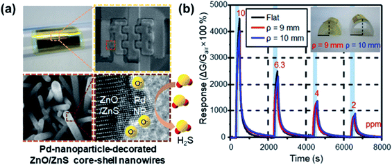 |
| | Fig. 29 (a) Photograph and SEM and TEM images of a ZnO/ZnS NW sensor on a flexible substrate and (b) the H2S gas sensing result. Reprinted with permission from ref. 132. Copyright 2019, ACS Publishing. | |
Table 9 Gas sensing properties of metal sulfide-based sensors for inorganic gases
| Material |
Structure |
Synthesis method |
Analyte |
Concentration |
Response (%) |
LOD |
τ
s/τr |
OT (°C) |
Ref. |
| CIS/ZnS (optical) |
QDs |
Hydrothermal method |
CO2 |
100 vol% |
1240* |
— |
— |
RT |
223
|
| QDs |
Hydrothermal method |
100 vol% |
99.6 |
— |
— |
RT |
224
|
| CdSe/ZnS (optical) |
QDs |
Hydrothermal method |
CO2 |
100 vol% |
84* |
— |
— |
RT |
225
|
| MoS2 |
NPs |
Chemical exfoliation |
O2 |
2 vol% |
769* |
49.96 ppb |
— |
300 |
226
|
| GaS |
NSs |
ME |
O2 |
— |
— |
— |
— |
— |
230
|
| SnS2 |
2D flakes |
Wet-chemical method |
O2 |
2 vol% |
160* |
— |
10 min/15 min |
130 (UV) |
227
|
| SnS–SnO2 |
Nanocomposite |
Electrochemical deposition |
O2 |
19 ppm |
21000 |
900 ppb |
52 s/38 s |
128 |
228
|
| PbS |
QDs |
Deposition |
H2S |
500 ppm |
421700* |
— |
23 s/171 s |
135 |
101
|
| CuS/CuO |
Nanocomposite |
Solvothermal method |
H2S |
1.88% |
313900 |
— |
75 s/67 s |
RT |
229
|
| ZnS/ZnO |
Nanocomposite |
Hydrothermal method |
H2S |
10 ppm |
4491 |
|
99 s/88 s |
95 |
132
|
| CdS |
2D flakes |
Wet-chemical method |
SO2 |
100 ppm |
— |
— |
15 min/NA |
400 |
106
|
| Ni-doped MoS2 |
NFWs |
Hydrothermal method |
SO2 |
5 ppm |
7.4 |
250 ppb |
51 s/73 s |
RT |
90
|
4.2.5 H2.
H2 is a colorless, tasteless, odorless, and flammable gas. It is an excellent candidate carrier in the clean energy area, such as for automobile engines and fuel cells. Thus it requires high-performance H2 sensors in mobile transportation as well as household environments. Hafeez et al.231 compared and analyzed the H2 gas-sensing performance of ZnS nanostructures with different morphologies (NWs, nanodots (NDs), and nanoleaves (NLs)). They found that NWs have higher cohesive energy than others, which showed a response% of 800% towards 50000 ppm H2 gas at an OT of 230 °C. Sabah et al.104 prepared a CuS thin film by spray pyrolysis deposition using deionized water and used it for the detection of H2 gases. Linganiso et al.105 synthesized NiS nanostructures and measured the H2 gas sensitivity, which has 158% response to 100 ppm H2 at 300 °C. Baek and Kim107 fabricated an H2 sensor with few-layered Pd-doped MoS2, which exhibited a 35.3% response% when exposed to a 1% H2-containing gas. In contrast, the pristine MoS2 showed no reaction. Perrozzi et al.215 demonstrated that the H2 gas sensor based on WS2/WO3 hierarchical heterostructures with surface oxygen and sulfur vacancies had a high response% of 430% towards 500 ppm H2 and exhibited a low LOD of 1 ppm. The sensors showed no substantial humidity cross-sensitivity effects, indicating the great potential application in real-world H2 detection. Various metal sulfide-based H2 gas sensors are listed in Table 10.
Table 10 Gas sensing properties of metal sulfide-based sensors for H2
| Material |
Structure |
Synthesis method |
Concentration |
Response (%) |
LOD (ppm) |
τ
s/τr |
OT (°C) |
Ref. |
| ZnS |
Nanostructures |
PVD |
50000 ppm |
800 |
— |
— |
230 |
231
|
| CuS |
Film |
Spray pyrolysis |
1000 ppm |
9890 |
— |
16/34 s |
RT |
104
|
| Au-coated NiS |
Nanostructures |
Hydrothermal method |
95% |
58* |
— |
∼50 s/∼100 s |
300 |
105
|
| Pd-doped MoS2 |
NSs |
Solution processing |
1% |
35.3 |
50 |
∼500 s/∼1200 s |
RT |
107
|
| WS2/WO3 |
Nanocomposites |
Oxidation |
500 ppm |
430* |
1 |
— |
150 |
215
|
4.2.6 Humidity sensor.
Humidity sensors have been successfully used in various fields, such as environmental monitoring, industrial production, and the medical instrumentation field. Tang et al.71 demonstrated that SnS NFKs could be used for real-time respiration detection due to their high response% of 2491000% and fast response/recovery time (6 s/4 s), suitable for health monitoring, see Fig. 30. Guo et al. fabricated transparent and flexible WS2 based humidity sensors for electronic skin, with a wide relative humidity range (up to 90%) with fast response and recovery in a few seconds.232 Feng et al.233 fabricated a flexible touchless positioning interface based on a highly sensitive VS2 NS humidity sensor. However, VS2 ultrathin NSs have poor stability. To improve the stability, Chen et al. proposed a MoS2/VS2 (ref. 35) sensor; after 30 days its response% was maintained at around 579750%, indicating that the nanocomposite sensor has good long-term stability. Chemiresistor sensors based on ReS2 NSs234 and MoS2 decorated with Pt NPs235 were reported. The Pt–MoS2 sensor showed a high and stable response% of 400000% at 85% RH when tested over a few months.
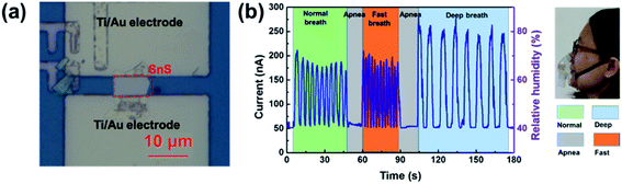 |
| | Fig. 30 (a) Optical image of a SnS nanoflake-based sensor. (b) Real-time respiration detection by using a SnS humidity sensor. Reprinted with permission from ref. 71. Copyright 2019, © IOP Publishing. All rights reserved. | |
Apart from the chemiresistor sensor, the optical, impedance, and capacitive sensors were employed for the detection of humidity. Luo et al.236 and Li et al.138 demonstrated all-fibre-optic humidity sensors comprising a WS2 and MoS2 film overlay on an SPF, respectively. They used a 1550 nm laser with SPF, which removes a portion of the cladding to form a polished region; propagated light confined in the core can escape out to this polished surface via evanescent waves, giving rise to strong interactions between light and the external environment. The responses of different types of fibre-optic humidity sensors are listed in Table 11. It is found that the MoS2-coated SPF sensor has a high response, and the MoS2-coated ESMF has a fast response time, which enables the fibre-optic sensor to monitor different breathing patterns of human beings. The impedance and capacitive humidity sensors are listed in Table 12. All of them show ultra-high sensing response, for instance, the sensing response of SmFeO3-modified MoS2 nanocomposites is more than five orders of magnitude (10598100%) within the whole RH range of 11% to 95% RH at 10 Hz. Moreover, the combination of a polymeric material, poly(3,4-ethylenedioxythiophene) polystyrene sulfonate (PEDOT:PSS), and MoS2 2D NFKs gives a humidity sensor with an ultra-fast response and excellent recovery with values of 0.5 s and 0.8 s, respectively.
Table 11 The humidity sensing performances of fibre-optic sensing devices in the literature
| Device structure |
τ
s (s) |
τ
r (s) |
Dynamic range of response |
Ref. |
| MoS2-coated ESMF |
0.066 |
2.395 |
0.487 dB/(20–80% RH) |
237
|
| MoS2-coated SPF |
0.85 |
0.85 |
13.5 dB/(40–85% RH) |
138
|
| WS2-coated SPF |
1 |
4 |
9 dB/(37–90% RH) |
236
|
Table 12 Comparison of different metal sulfide-based humidity sensors
| Material |
Structure |
Synthesis method |
Type |
RH range (%) |
Response (%) or Sensitivity |
τ
s/τr |
OT (°C) |
Ref. |
| SnS |
Nanoflakes |
LPE |
Resistive |
3–99 |
2491000 (99% RH) |
6 s/4 s |
RT |
71
|
| WS2 |
Thin film |
CVD |
Resistive |
25–90 |
235600* (90% RH) |
∼5 s/∼6 s |
RT |
232
|
| ReS2 |
Nanosheets |
CVD |
Resistive |
30–80 |
600 (70% RH) |
20 s/10 s |
RT |
234
|
| VS2 |
Nanosheets |
LPE |
Resistive |
0–90 |
2900* (90% RH) |
30–40 s/12–50 s |
RT |
233
|
| Pt–MoS2 |
NFKs |
Solution methods |
Resistive |
35–85 |
400000 (85% RH) |
91.2 s/153.6 s |
RT |
235
|
| TaS2 |
Nanosheets |
CVD |
Impedance |
11–95 |
20190 (11% RH) |
0.6 s/2 s |
RT |
238
|
| MoS2 |
Nanospheres |
Hydrothermal method |
Capacitive |
17.2–89.5 |
81.9 pF/% RH (sensitivity) |
140 s/80 s |
RT |
239
|
| MoS2 |
QDs |
LPE |
Impedance |
10–95 |
2.21 MΩ/% RH (sensitivity) |
14 s |
RT |
240
|
| MoS2/VS2 |
Nanocomposite |
Hydrothermal method |
Impedance |
11–95 |
579750* (95% RH) |
23 s/13 s |
RT |
35
|
| MoS2/ZnO |
Nanocomposites |
Hydrothermal & chemical method |
Impedance |
11–95 |
— |
1 s/20 s |
RT |
241
|
| MoS2/Ag |
Nanocomposites |
Mixture dispersion |
Capacitive |
11–97 |
21112 pF/% RH (sensitivity) |
∼1.5 s |
RT |
242
|
| MoS2/SnO2 |
Nanocomposite |
Hydrothermal method |
Capacitive |
0–97 |
3285000 (97% RH) |
5/13 s |
RT |
243
|
| SmFeO3@MoS2 |
Nanocomposites |
Hydrothermal method |
Impedance |
11–95 |
10598100* (95% RH) |
1.5 s/29.8 s |
RT |
244
|
| PEDOT:PSS/MoS2 |
Nanocomposites |
Exfoliation & deposition |
Impedance |
0–80 |
50 kΩ/% RH, 850 Hz/% RH (sensitivity) |
0.5 s/0.8 s |
RT |
245
|
| SnS2/GO |
Nanocomposites |
Solvothermal method, mixture |
Impedance |
11–97 |
6539600 (97% RH) |
0.9 s/10 s |
RT |
246
|
| SnS2/TiO2 |
Nanohybrid film |
LBL self-assembly |
Impedance |
11–97 |
442000 Ω/% RH (sensitivity) |
<58 s |
RT |
247
|
| SnS2/Zn2SnO4 |
Nanohybrid |
Solvothermal method |
Capacitive |
0–97 |
10709 pF/% RH (sensitivity) |
18 s/1 s |
RT |
248
|
| ZnO NDs/WS2 |
Heterostructure |
Evaporation |
Capacitive |
18–85 |
101.71 fF/% RH (sensitivity) |
74.51 s/25.67 s |
RT |
249
|
| WS2/SnO2 |
Nanocomposites |
LBL self-assembly |
Capacitive |
11–97 |
14125900 (97% RH) |
100 s/100 s |
RT |
250
|
| 21112 pF/% RH (sensitivity) |
All the mentioned metal sulfide-based humidity sensors can work at room temperature, leading to wearable electronics applications. Among these four types of humidity sensors, fibre-optic sensors have ultrafast response speed and low response and a complex measurement setup. However, it is necessary to find a way to easily integrate the fibre-optic sensor into one package that can be used for gas testing. Besides, humidity sensors can not only be used to monitor the patient's respiration profile continuously but also to determine the dehydration state. Highly sensitive and fast response and recovery humidity sensors are urgently required in real-world applications.
5. Summary and perspectives
This review shows a systematic summary of the crystal structure and gas sensing mechanism of metal sulfide nanomaterials, as well as the gas-sensing performance of metal sulfide-based devices. Here, to summarise the state-of-the-art metal sulfide gas sensors and analyse future and perspectives of the metal sulfide sensor market, we further provide a brief Strengths–Weaknesses–Opportunities–Threats (SWOT) analysis of metal sulfide technology for gas sensing.
5.1 Strengths
(1) Mechanism analysis. This is an efficient way to analyze and predict the gas sensing properties by combining theoretical (DFT) and experimental (i.e., materials characterization and gas testing) methods. For instance, the higher the adsorption energy, the higher the selectivity toward this kind of gas molecule; the ELF plot can reflect the chemical bond between the gas molecule and metal sulfides, which affect the nature of physisorption and chemisorption and further influence the recovery time of the device; the charge transfer between the gases and metal sulfides can reveal the donor or acceptor of the gases, which is associated with the change of conductivity.
(2) Improvements in gas sensing performance.
(i) Functionalization of metal sulfides. To further improve the sensitivity, doping and defect substitution are the most commonly used tools in functionalization and are efficient methods to change the band structure, modify the electronic and transport properties, and enhance the gas sensing applications. However, most of the gas sensing behaviours of functionalized metal sulfides were analyzed through DFT calculations. There are a lack of experimental reports on the influence of defects on the metal sulfide-based devices' gas-sensing performance.
(ii) Schottky junction and heterojunction gas sensors. They are based on band alignment theory, which can significantly improve the gas sensing response and LOD. Most of them have excellent sensing performances, including high response, fast response time, wide detection range, and low LOD. Thus, more people are focusing on junction-based gas sensors.
(iii) FET gas sensors. Most FET gas sensors ultimately modify the sensitivity towards a target gas by changing the energy landscape of the sensor surface. This type of sensing device has been used to detect many types of gases, such as CO, NO, NH3, NO2, SO2, H2, and VOCs. However, most of the FET gas sensors are still not satisfactory in the aspects of device instability and limited large-scale production, even though they have a fast response and selectivity.
(iv) Other sensing mechanisms. The optical gas sensor has been employed to detect non-polar gases, such as CH4, due to its high accuracy. Most of them are fibre optic gas sensors based on the reduction in the effective refractive index and showed high selectivity to methanol among VOCs. SAW gas sensors can detect a low concentration of NO2 gas at room temperature with good efficiency and selectivity, and they are coated with polymers for the identification of breath biomarkers and the diagnosis of various diseases.
(3) Applications. Suitable applications for each type of gas sensor are found according to the specific gas-sensing performance of various metal sulfides. It is found that the IV–VI compound pristine metal sulfides, such as SnS, PbS, and GeS, show fast response and recovery time. The II–VI compound semiconductors, such as CdS and ZnS, have high response and selectivity to VOCs. However, most of their OTs are relatively high. Most of the transition metal sulfides have a larger electronegativity, potentially increasing the number of gas adsorption sites, and have been used for gas sensing of NOx, NH3, O2, and ethanol. With respect to VOCs, various pristine metal sulfides can be used for the detection of acetone, while functionalized or heterojunction-based metal sulfides are applied for sensing benzene, methane, formaldehyde, ethanol, and LPG. Most of them work at low temperatures, except for the detection of ethanol, whose OT is usually higher than 150 °C. In the aspect of inorganic gases, all types of metal sulfides are used for sensors. Heterojunction-based and FET-based metal sulfide devices are promising candidates for gas sensing. They can take advantage of metal sulfide and other materials (such as metal, dissimilar metal sulfide, metal oxide, and organic materials) as well as the field-effect induced by back gate bias. The large surface to volume ratio combined with significant changes in the measured signals upon gas adsorption induce high sensitivity and selectivity and low LOD. Besides, to improve their performance, researchers used light illumination to stimulate the charge transfer between the gas molecules and metal sulfide.251 Thus, the light source can be integrated into the device in the future.
5.2 Weaknesses
(1) Lack of a low LOD. Biomarkers, such as NOx, NH3, and CH4, are at hundreds or tens of ppb in people. It is challenging to detect lung diseases, i.e., asthma, by the detection of NOx in exhaled breath. MoS2/ZnO has the lowest LOD for NH3, which is 12 ppb. Au/Gr–MoS2–Gr/Au can detect 0.1 ppb NO2, and Ni-doped MoS2 can detect 250 ppb SO2. For VOCs, α-Fe2O3/MoS2 has a LOD of 1 ppm toward ethanol at room temperature. However, it is not as low as the LOD requirement for biomarker detection.
(2) Insufficient gas selectivity. Most gas testing reported in previous work was conducted in dry atmospheres. In contrast, the working environment may be under high humidity conditions in the real world; for instance, exhaled human breath contains almost saturated moisture; the RH level is higher in the basin area. This thereby affects the sensitivity and selectivity of sensors. The effect of humidity could be reduced significantly by using a moisture absorber, increasing the OT, or optimizing the morphology or architecture of the materials. However, it is challenging to distinguish the specified concentration of the target gas in a mixture. For instance, the automobile exhaust pollutants primarily include CO, hydrocarbons, NO, SO2, particles (i.e., some lead compounds, oil mist, and heavy metal compounds), and odour (i.e., formaldehyde). The large-sized particles may cover the surface of the material and further affect the response to NO, CO, or SO2. Similarly, in the aspect of lung cancer detection, because there is no single biomarker for lung cancer, it is much more difficult than detecting asthma, diabetes, and halitosis. More work needs to be done in this field.
(3) Lack of reproducibility. 2D/nanostructured metal sulfides have large surface areas and abundant adsorption sites, which possess high adsorption energies towards gas molecules, especially chemisorbed gases. It is challenging to desorb them from the metal sulfides without external stimulation (high temperature, high bias voltage, or light illumination). Therefore, the devices could not be recovered to the initial state. Besides, the experimental conditions are hard to reproduce, and there are a lack of standardized methods to carry out the testing. Moreover, the absence of standardization, quality assurance, and reliable benchmarking are still crucial issues that hinder the applications of metal sulfides in the healthcare area.
(4) Lack of precise mechanism analysis. Most of the reported mechanisms are analyzed through DFT calculations. Sometimes, the simulation model cannot consider every detail shown in the experiment, which induces deviations between the simulation and experimental results. It is necessary to find an efficient tool or method to realize the benchmark.
All metal sulfide-based devices face the same problem as all solid-state sensors, such as translation from academic to industrial research, reproducibility of the lab conditions, batch production, integration/communication/power supply and real-world detection.
5.3 Opportunities
(1) New nanomaterials are emerging. Nanostructured metal sulfides with different forms, such as nanowires, nanoflowers, nanopores, and nanorods; or combined with hybrid materials, e.g., materials decorated with metal or semiconductor particles, Schottky junctions with a metal layer or CNMs, and heterostructures with hBN, MXene, and MOFs; or those using novel substrates, such as PVP, PI, PDMS, and other flexible substrates, can help to realize skin patching of human beings or can be integrated into a textile.
(2) The matching between materials and circuit electrodes, such as the energy band and work function, needs to be considered in terms of device design. Meanwhile, real-time detection applications, signal processing, low energy consumption, intelligent operation, and integration with sensor networks (e.g., internet of things) need to be considered. The combinations of 2D gas sensors with artificial intelligence in smart cities, smart homes, and smart hospitals are hot topics for the future.
(3) FET devices can effectively improve the gas sensing performance, but it is necessary to control their energy consumption and turn-on voltage reasonably in the future. Device performance can be enhanced by designing the device structure (shape and size of gate-drain electrodes), selecting the dielectric layer, and selecting the substrate. Some metal sulfides (such as MoS2 and WS2) could play an important role in electronics for logic, memory, and connections, enabling the extension of Moore's law,252 as well as the Paradigm of “More than Moore”.253,254 There are primarily three challenges for these materials to meet industry needs in practical devices, such as the accuracy of the predicting properties, the methods of growing and testing high-quality materials, and the assessment of the device's performance.
5.4 Threats
The improvements of metal sulfide-based nanomaterials and other nanotechnologies in the gas-sensing performance are still being analyzed. The equipment used for the nanomaterial-based device should be different from those for traditional Si-based devices. For the future, the application of new nanomaterial devices still has a long way to go. For example, the current of the metal sulfide device is too small, and it is necessary to implement signal acquisition and intelligent control through a precise amplifier circuit. Defective materials are difficult to desorb, and additional UV light sources are needed to achieve rapid desorption, increasing the overall size and cost of the device. Time will be needed to reach market readiness and to overcome the reluctance to accept and introduce new technology, which now remains a severe hindrance in incorporating the production chain.
In this review, we listed the latest progress made in improving the field of 2D-metal sulfide-based gas sensors to overview the developments seen in this area extending from crystal features to device engineering. The crystal structures of metal sulfides and the gas sensing mechanism based on DFT analysis are introduced first. Various types of metal sulfide-based gas-sensing devices, including chemiresistors, functionalized-metal sulfides, Schottky diodes, heterojunctions, field-effect transistors, and optical, impedance, capacitive and SAW sensors, are compared and presented. We then discuss the extensive applications of metal sulfide-based sensors in gas sensing. Various gas sensors for the detection of VOC biomarkers (e.g., acetone, benzene, methane, formaldehyde, and ethanol) and inorganic gases (e.g., CO2, NH3, H2S, NO, and humidity) were discussed. There is a fabulous opportunity right now for developing 2D metal sulfides as gas sensors and use them for gas sensing, even integrated into the IoT system. However, they still have some shortcomings that need to be overcome, such as a high LOD, effect of a high humidity environment, insufficient gas selectivity, and low reproducibility in gas detection. It is necessary to develop new materials or construct advanced nanostructures to improve the performances. Additionally, from a device architecture perspective, implementation of the new signal-processing technology and recognition algorithms based on a single-chip system using multiplex detection channels is a significant and promising route for the development of gas sensing platforms.
Conflicts of interest
The authors declare no conflict of interest.
References
- J. Zhang, X. Liu, G. Neri and N. Pinna, Adv. Mater., 2016, 28, 795–831 CrossRef.
- A. Afroozeh, E. Akbari and P. Yupapin, J. Nanoelectron. Optoelectron., 2019, 14, 1225–1229 CrossRef.
- S. Feng, F. Farha, Q. Li, Y. Wan, Y. Xu, T. Zhang and H. Ning, Sensors, 2019, 19, 3760 CrossRef.
- S. Das and M. Pal, J. Electrochem. Soc., 2020, 167, 037562 CrossRef CAS.
- S. Orzechowska, A. Mazurek, R. Świsłocka and W. Lewandowski, Materials, 2019, 13, 80 CrossRef.
- A. Roine, E. Veskimäe, A. Tuokko, P. Kumpulainen, J. Koskimäki, T. A. Keinänen, M. R. Häkkinen, J. Vepsäläinen, T. Paavonen, J. Lekkala, T. Lehtimäki, T. L. Tammela and N. K. J. Oksala, J. Urol., 2014, 192, 230–235 CrossRef.
- J.-C. Juncker, Official Journal of the European Union, 2017, 6, 115–120 Search PubMed , https://eur-lex.europa.eu/legal-content/EN/TXT/?uri=uriserv%3AOJ.L_.2017.027.01.0115.01.ENG.
- D. J. Buckley, N. C. G. Black, E. G. Castanon, C. Melios, M. Hardman and O. Kazakova, 2D Mater., 2020, 7, 032002 CrossRef CAS.
- G. Korotcenkov, Mater. Sci. Eng., B, 2007, 139, 1–23 CrossRef CAS.
- Y. Pang, J. Jian, T. Tu, Z. Yang, J. Ling, Y. Li, X. Wang, Y. Qiao, H. Tian, Y. Yang and T.-L. Ren, Biosens. Bioelectron., 2018, 116, 123–129 CrossRef CAS.
- L. Sacco, S. Forel, I. Florea and C.-S. Cojocaru, Carbon, 2020, 157, 631–639 CrossRef CAS.
- V. Schroeder, S. Savagatrup, M. He, S. Lin and T. M. Swager, Chem. Rev., 2019, 119, 599–663 CrossRef CAS.
- H. T. Kim, H. Y. Kim, Y. S. Park, Y. S. Kim and W. H. Jang, Chemosensors, 2017, 5, 15 CrossRef.
-
N. Taguchi, Japanese patent, 4538200, 1962.
- W.-T. Koo, S.-J. Choi, N.-H. Kim, J.-S. Jang and I.-D. Kim, Sens. Actuators, B, 2016, 223, 301–310 CrossRef CAS.
- D. Kwak, M. Wang, K. J. Koski, L. Zhang, H. Sokol, R. Maric and Y. Lei, ACS Appl. Mater. Interfaces, 2019, 11, 10697–10706 CrossRef CAS.
- J.-S. Jang, S.-J. Choi, S.-J. Kim, M. Hakim and I.-D. Kim, Adv. Funct. Mater., 2016, 26, 4740–4748 CrossRef CAS.
- W. Liu, L. Xu, K. Sheng, X. Zhou, B. Dong, G. Lu and H. Song, NPG Asia Mater., 2018, 10, 293–308 CrossRef CAS.
- Y. Chen, L. Yu, Q. Li, Y. Wu, Q. Li and T. Wang, Nanotechnology, 2012, 23, 415501 CrossRef.
-
Y. Deng, Semiconducting Metal Oxides for Gas Sensing, Springer, 2019 Search PubMed.
-
E. Gabal, S. Chatterjee, F. K. Ahmed and K. A. Abd-Elsalam, in Carbon Nanomaterials for Agri-Food and Environmental Applications, ed. K. A. Abd-Elsalam, Elsevier, 2020, pp. 133–153, DOI:10.1016/B978-0-12-819786-8.00007-4.
- C. R. Minitha, V. S. Anithaa, V. Subramaniam and R. T. Rajendra Kumar, ACS Omega, 2018, 3, 4105–4112 CrossRef CAS.
- R. Sha, S. K. Puttapati, V. V. S. S. Srikanth and S. Badhulika, J. Electroanal. Chem., 2017, 785, 26–32 CrossRef CAS.
- S. Kubendhiran, S. Sakthinathan, S.-M. Chen, P. Tamizhdurai, K. Shanthi and C. Karuppiah, J. Colloid Interface Sci., 2017, 497, 207–216 CrossRef CAS.
- F. Rigoni, S. Tognolini, P. Borghetti, G. Drera, S. Pagliara, A. Goldoni and L. Sangaletti, Analyst, 2013, 138, 7392–7399 RSC.
- E. Singh, M. Meyyappan and H. S. Nalwa, ACS Appl. Mater. Interfaces, 2017, 9, 34544–34586 CrossRef CAS.
- E. Lee, Y. S. Yoon and D.-J. Kim, ACS Sens., 2018, 3, 2045–2060 CrossRef CAS.
- C.-H. Lai, M.-Y. Lu and L.-J. Chen, J. Mater. Chem., 2012, 22, 19–30 RSC.
- M. Donarelli, S. Prezioso, F. Perrozzi, F. Bisti, M. Nardone, L. Giancaterini, C. Cantalini and L. Ottaviano, Sens. Actuators, B, 2015, 207, 602–613 CrossRef CAS.
- Z. Tian, C. Guo, M. Zhao, R. Li and J. Xue, ACS Nano, 2016, 11, 2219 CrossRef.
- A. S. Rodin, L. C. Gomes, A. Carvalho and A. H. Castro Neto, Phys. Rev. B, 2016, 93, 045431 CrossRef.
- S. Zhang, N. Wang, S. Liu, S. Huang, W. Zhou, B. Cai, M. Xie, Q. Yang, X. Chen and H. Zeng, Nanotechnology, 2016, 27, 274001 CrossRef.
- J. Wang, G. Lian, Z. Xu, C. Fu, Z. Lin, L. Li, Q. Wang, D. Cui and C.-P. Wong, ACS Appl. Mater. Interfaces, 2016, 8, 9545–9551 CrossRef CAS.
- M. F. Afsar, M. A. Rafiq and A. I. Y. Tok, RSC Adv., 2017, 7, 21556–21566 RSC.
- X. Chen, K. Yu, Y. Shen, Y. Feng and Z. Zhu, ACS Appl. Mater. Interfaces, 2017, 9, 42139–42148 CrossRef CAS.
- W. Zhou, X. Zou, S. Najmaei, Z. Liu, Y. Shi, J. Kong, J. Lou, P. M. Ajayan, B. I. Yakobson and J.-C. Idrobo, Nano Lett., 2013, 13, 2615–2622 CrossRef CAS.
- J. Zhu, H. Zhang, Y. Tong, L. Zhao, Y. Zhang, Y. Qiu and X. Lin, Appl. Surf. Sci., 2017, 419, 522–530 CrossRef CAS.
- F. K. Perkins, A. L. Friedman, E. Cobas, P. M. Campbell, G. G. Jernigan and B. T. Jonker, Nano Lett., 2013, 13, 668–673 CrossRef CAS.
- Z. Ashkavand, E. Sadeghi, R. Parvizi and M. Zare, ACS Appl. Mater. Interfaces, 2020, 12, 34283–34296 CrossRef CAS.
- S. Chandrasekaran, L. Yao, L. Deng, C. Bowen, Y. Zhang, S. Chen, Z. Lin, F. Peng and P. Zhang, Chem. Soc. Rev., 2019, 48, 4178–4280 RSC.
- Y. Cui, Z. Zhou, T. Li, K. Wang, J. Li and Z. Wei, Adv. Funct. Mater., 2019, 29, 1900040 CrossRef.
- S. Manzeli, D. Ovchinnikov, D. Pasquier, O. V. Yazyev and A. Kis, Nat. Rev. Mater., 2017, 2, 17033 CrossRef CAS.
- W. Choi, N. Choudhary, G. H. Han, J. Park, D. Akinwande and Y. H. Lee, Mater. Today, 2017, 20, 116–130 CrossRef CAS.
- J. Ping, Z. Fan, M. Sindoro, Y. Ying and H. Zhang, Adv. Funct. Mater., 2017, 27, 1605817 CrossRef.
- Z. Xie, D. Wang, T. Fan, C. Xing, Z. Li, W. Tao, L. Liu, S. Bao, D. Fan and H. Zhang, J. Mater. Chem. B, 2018, 6, 4747–4755 RSC.
- S. Kouser, A. Thannikoth, U. Gupta, U. V. Waghmare and C. N. R. Rao, Small, 2015, 11, 4723–4730 CrossRef CAS.
- R. M. Martin, Phys. Rev. B: Solid State, 1970, 1, 4005–4011 CrossRef.
- V. Lantto and V. Golovanov, Sens. Actuators, B, 1995, 25, 614–618 CrossRef CAS.
- Y. Rodríguez-Lazcano, H. Martínez, M. Calixto-Rodríguez and A. Núñez Rodríguez, Thin Solid Films, 2009, 517, 5951–5955 CrossRef.
- D. G. Bell, D. M. Hum, L. Pincherle, D. W. Sciama, P. M. Woodward and N. F. Mott, Proc. R. Soc. London, Ser. A, 1953, 217, 71–91 CAS.
- J. Tian and G. Cao, Nano Rev., 2013, 4, 22578 CrossRef.
- J. Trahan, R. G. Goodrich and S. F. Watkins, Phys. Rev. B: Solid State, 1970, 2, 2859–2863 CrossRef.
- Z. Wang, S. Ning, T. Fujita, A. Hirata and M. Chen, ACS Nano, 2016, 10, 10308–10316 CrossRef CAS.
- A. Splendiani, L. Sun, Y. Zhang, T. Li, J. Kim, C.-Y. Chim, G. Galli and F. Wang, Nano Lett., 2010, 10, 1271–1275 CrossRef CAS.
- T. A. J. Loh and D. H. C. Chua, J. Phys. Chem. C, 2015, 119, 27496–27504 CrossRef CAS.
- L. A. Burton, D. Colombara, R. D. Abellon, F. C. Grozema, L. M. Peter, T. J. Savenije, G. Dennler and A. Walsh, Chem. Mater., 2013, 25, 4908–4916 CrossRef CAS.
- L. Li, X. Fang, T. Zhai, M. Liao, U. K. Gautam, X. Wu, Y. Koide, Y. Bando and D. Golberg, Adv. Mater., 2010, 22, 4151–4156 CrossRef CAS.
- K. Xu, Z. Wang, F. Wang, Y. Huang, F. Wang, L. Yin, C. Jiang and J. He, Adv. Mater., 2015, 27, 7881–7887 CrossRef CAS.
- Y. Kim, K. C. Kwon, S. Kang, C. Kim, T. H. Kim, S.-P. Hong, S. Y. Park, J. M. Suh, M.-J. Choi, S. Han and H. W. Jang, ACS Sens., 2019, 4, 2395–2402 CrossRef CAS.
- Q. He, Q. Ma, B. Chen, Z. Yin, Z. Zeng, S. Wu, X. Cao, X. Kong and H. Zhang, APL Mater., 2014, 2, 092506 CrossRef.
- S. Liu, W. Xiao, M. Zhong, L. Pan, X. Wang, H.-X. Deng, J. Liu, J. Li and Z. Wei, Nanotechnology, 2018, 29, 184002 CrossRef.
- N. Rafiefard, A. Iraji zad, A. Esfandiar, P. Sasanpour, S. Fardindoost, Y. Zou, S. J. Haigh and S. H. H. Shokouh, Microchim. Acta, 2020, 187, 117 CrossRef CAS.
- Y.-R. Tao, X.-C. Wu and W.-W. Xiong, Small, 2014, 10, 4905–4911 CrossRef CAS.
- W.-W. Xiong, J.-Q. Chen, X.-C. Wu and J.-J. Zhu, J. Mater. Chem. C, 2014, 2, 7392–7395 RSC.
- C. C. Mayorga-Martinez, Z. Sofer, J. Luxa, Š. Huber, D. Sedmidubský, P. Brázda, L. Palatinus, M. Mikulics, P. Lazar, R. Medlín and M. Pumera, ACS Nano, 2018, 12, 464–473 CrossRef CAS.
- W. Huang, L. Gan, H. Yang, N. Zhou, R. Wang, W. Wu, H. Li, Y. Ma, H. Zeng and T. Zhai, Adv. Funct. Mater., 2017, 27, 1702448 CrossRef.
- U. G. E. Perera, H. J. Kulik, V. Iancu, L. G. G. V. Dias da Silva, S. E. Ulloa, N. Marzari and S. W. Hla, Phys. Rev. Lett., 2010, 105, 106601 CrossRef CAS.
- C. Xu, X. Huang, X. Xu, X. Zhang and H. Zhang, Int. J. Quantum Chem., 2020, 120, e26120 CAS.
- A. Savin, R. Nesper, S. Wengert and T. F. Fässler, Angew. Chem., Int. Ed. Engl., 1997, 36, 1808–1832 CrossRef CAS.
- J. K. Burdett and T. A. McCormick, J. Phys. Chem. A, 1998, 102, 6366–6372 CrossRef CAS.
- H. Tang, Y. Li, H. Ye, f. Hu, C. Gao, L.-Q. Tao, T. Tu, G. Gou, X. Chen, X. Fan, T.-L. Ren and G. Zhang, Nanotechnology, 2019, 31, 055501 CrossRef.
- F. Hu, H. Tang, C. Tan, H. Ye, X. Chen and G. Zhang, IEEE Electron Device Lett., 2017, 38, 983–986 CAS.
- S.-J. Choi and I.-D. Kim, Electron. Mater. Lett., 2018, 14, 221–260 CrossRef CAS.
- Q. Yue, Z. Shao, S. Chang and J. Li, Nanoscale Res. Lett., 2013, 8, 425 CrossRef.
- S. Zhao, J. Xue and W. Kang, Chem. Phys. Lett., 2014, 595–596, 35–42 CrossRef CAS.
- J. Cha, K.-A. Min, D. Sung and S. Hong, Curr. Appl. Phys., 2018, 18, 1013–1019 CrossRef.
- S. Ma, D. Yuan, Y. Wang and Z. Jiao, J. Mater. Chem. C, 2018, 6, 8082–8091 RSC.
- D. B. Putungan, S.-H. Lin and J.-L. Kuo, Phys. Chem. Chem. Phys., 2015, 17, 21702–21708 RSC.
- Y. Linghu and C. Wu, J. Phys. Chem. C, 2019, 123, 10339–10345 CrossRef CAS.
- Q. Tang and D.-e. Jiang, Chem. Mater., 2015, 27, 3743–3748 CrossRef CAS.
- Z. Qin, D. Zeng, J. Zhang, C. Wu, Y. Wen, B. Shan and C. Xie, Appl. Surf. Sci., 2017, 414, 244–250 CrossRef CAS.
- H. Li, Z. Yin, Q. He, H. Li, X. Huang, G. Lu, D. W. H. Fam, A. I. Y. Tok, Q. Zhang and H. Zhang, Small, 2012, 8, 63–67 CrossRef CAS.
- D. J. Late, Y.-K. Huang, B. Liu, J. Acharya, S. N. Shirodkar, J. Luo, A. Yan, D. Charles, U. V. Waghmare, V. P. Dravid and C. N. R. Rao, ACS Nano, 2013, 7, 4879–4891 CrossRef CAS.
- Y. Li, X. Zhang, D. Chen, S. Xiao and J. Tang, Appl. Surf. Sci., 2018, 443, 274–279 CrossRef CAS.
- H. Luo, Y. Cao, J. Zhou, J. Feng, J. Cao and H. Guo, Chem. Phys. Lett., 2016, 643, 27–33 CrossRef CAS.
- H. Wei, Y. Gui, J. Kang, W. Wang and C. Tang, Nanomaterials, 2018, 8, 646 CrossRef.
- A. Sharma, Anu, M. S. Khan, M. Husain, M. S. Khan and A. Srivastava, IEEE Sens. J., 2018, 18, 2853–2860 CAS.
- D. Ma, W. Ju, T. Li, X. Zhang, C. He, B. Ma, Z. Lu and Z. Yang, Appl. Surf. Sci., 2016, 383, 98–105 CrossRef CAS.
- R. Zhang, D. Fu, J. Ni, C. Sun and S. Song, Chem. Phys. Lett., 2019, 715, 273–277 CrossRef CAS.
- D. Zhang, J. Wu, P. Li and Y. Cao, J. Mater. Chem. A, 2017, 5, 20666–20677 RSC.
- Y. Kadioglu, G. Gökoğlu and O. Üzengi Aktürk, Appl. Surf. Sci., 2017, 425, 246–253 CrossRef CAS.
- V. Q. Bui, T.-T. Pham, D. A. Le, C. M. Thi and H. M. Le, J. Phys.: Condens. Matter, 2015, 27, 305005 CrossRef.
- C. Zhou, W. Yang and H. Zhu, J. Chem. Phys., 2015, 142, 214704 CrossRef.
- B. Zhao, C. Shang, N. Qi, Z. Y. Chen and Z. Q. Chen, Appl. Surf. Sci., 2017, 412, 385–393 CrossRef CAS.
- F. Li and C. Shi, Appl. Surf. Sci., 2018, 434, 294–306 CrossRef CAS.
- J. M. Jasmine, A. Aadhityan, C. Preferencial kala and D. J. Thiruvadigal, Appl. Surf. Sci., 2019, 489, 841–848 CrossRef CAS.
- H. Li, M. Huang and G. Cao, Phys. Chem. Chem. Phys., 2016, 18, 15110–15117 RSC.
- L. A. Currie, Anal. Chim. Acta, 1999, 391, 105–126 CrossRef CAS.
- J. Burgués, J. M. Jiménez-Soto and S. Marco, Anal. Chim. Acta, 2018, 1013, 13–25 CrossRef.
- S. T. Navale, D. K. Bandgar, M. A. Chougule and V. B. Patil, RSC Adv., 2015, 5, 6518–6527 RSC.
- H. Liu, M. Li, G. Shao, W. Zhang, W. Wang, H. Song, H. Cao, W. Ma and J. Tang, Sens. Actuators, B, 2015, 212, 434–439 CrossRef CAS.
- X.-H. Liu, P.-F. Yin, S. A. Kulinich, Y.-Z. Zhou, J. Mao, T. Ling and X.-W. Du, ACS Appl. Mater. Interfaces, 2017, 9, 602–609 CrossRef CAS.
- X. Wang, Z. Xie, H. Huang, Z. Liu, D. Chen and G. Shen, J. Mater. Chem., 2012, 22, 6845–6850 RSC.
- F. A. Sabah, N. M. Ahmed, Z. Hassan and H. S. Rasheed, Sens. Actuators, A, 2016, 249, 68–76 CrossRef.
- E. C. Linganiso, B. W. Mwakikunga, S. D. Mhlanga, N. J. Coville, B. T. Sone and M. Maaza, Sensors, 2012, 1–4 Search PubMed.
- N. Souda and Y. Shimizu, J. Mater. Sci., 2003, 38, 4301–4305 CrossRef.
- D.-H. Baek and J. Kim, Sens. Actuators, B, 2017, 250, 686–691 CrossRef.
- A. A. Ramanathan, IOP Conf. Ser.: Mater. Sci. Eng., 2018, 305, 012001 Search PubMed.
- Z. Qin, K. Xu, H. Yue, H. Wang, J. Zhang, C. Ouyang, C. Xie and D. Zeng, Sens. Actuators, B, 2018, 262, 771–779 CrossRef CAS.
- R. T. Tung, Appl. Phys. Rev., 2014, 1, 011304 Search PubMed.
- Y. Kim, S.-K. Kang, N.-C. Oh, H.-D. Lee, S.-M. Lee, J. Park and H. Kim, ACS Appl. Mater. Interfaces, 2019, 11, 38902–38909 CrossRef CAS.
- V. Van Quang, N. Van Dung, N. Sy Trong, N. Duc Hoa, N. Van Duy and N. Van Hieu, Appl. Phys. Lett., 2014, 105, 013107 CrossRef.
- X. Zheng, A. Calò, E. Albisetti, X. Liu, A. S. M. Alharbi, G. Arefe, X. Liu, M. Spieser, W. J. Yoo, T. Taniguchi, K. Watanabe, C. Aruta, A. Ciarrocchi, A. Kis, B. S. Lee, M. Lipson, J. Hone, D. Shahrjerdi and E. Riedo, Nat. Electron., 2019, 2, 17–25 CrossRef CAS.
- T. Pham, G. Li, E. Bekyarova, M. E. Itkis and A. Mulchandani, ACS Nano, 2019, 13, 3196–3205 CrossRef CAS.
- M.-L. Tsai, S.-H. Su, J.-K. Chang, D.-S. Tsai, C.-H. Chen, C.-I. Wu, L.-J. Li, L.-J. Chen and J.-H. He, ACS Nano, 2014, 8, 8317–8322 CrossRef.
-
T. Ihn, Semiconductor Nanostructures: Quantum States and Electronic Transport, Oxford University Press, 2010 Search PubMed.
- K. Xu, N. Li, D. Zeng, S. Tian, S. Zhang, D. Hu and C. Xie, ACS Appl. Mater. Interfaces, 2015, 7, 11359–11368 CrossRef.
- X. Wang, L. Huang, Y. Peng, N. Huo, K. Wu, C. Xia, Z. Wei, S. Tongay and J. Li, Nano Res., 2016, 9, 507–516 CrossRef.
- H. Yan, P. Song, S. Zhang, Z. Yang and Q. Wang, RSC Adv., 2015, 5, 79593–79599 RSC.
- X.-Q. Qiao, Z.-W. Zhang, D.-F. Hou, D.-S. Li, Y. Liu, Y.-Q. Lan, J. Zhang, P. Feng and X. Bu, ACS Sustainable Chem. Eng., 2018, 6, 12375–12384 CrossRef.
- Y. Han, Y. Ma, Y. Liu, S. Xu, X. Chen, M. Zeng, N. Hu, Y. Su, Z. Zhou and Z. Yang, Appl. Surf. Sci., 2019, 493, 613–619 CrossRef.
- X. Wang, Y. Sang, D. Wang, S. Ji and H. Liu, J. Alloys Compd., 2015, 639, 571–576 CrossRef CAS.
- S. Park, S. An, Y. Mun and C. Lee, ACS Appl. Mater. Interfaces, 2013, 5, 4285–4292 CrossRef CAS.
- W. Zeng, Y. Liu, J. Mei, C. Tang, K. Luo, S. Li, H. Zhan and Z. He, Sens. Actuators, B, 2019, 301, 127010 CrossRef CAS.
- A. Katoch, J.-H. Kim and S. S. Kim, ACS Appl. Mater. Interfaces, 2014, 6, 21494–21499 CrossRef CAS.
- G.-J. Sun, J. K. Lee, S. Choi, W. I. Lee, H. W. Kim and C. Lee, ACS Appl. Mater. Interfaces, 2017, 9, 9975–9985 CrossRef CAS.
- E. Espid and F. Taghipour, Sens. Actuators, B, 2017, 241, 828–839 CrossRef CAS.
- Z. Li, Y. Liu, D. Guo, J. Guo and Y. Su, Sens. Actuators, B, 2018, 271, 306–310 CrossRef CAS.
- Q. Zhang, S. Ma, R. Zhang, K. Zhu, Y. Tie and S. Pei, J. Alloys Compd., 2019, 807, 151650 CrossRef CAS.
- M. Li, W. Ren, R. Wu and M. Zhang, Sensors, 2017, 17, 1577 CrossRef.
- J. Zhai, L. Wang, D. Wang, H. Li, Y. Zhang, D. q. He and T. Xie, ACS Appl. Mater. Interfaces, 2011, 3, 2253–2258 CrossRef CAS.
- D. Yang, I. Cho, D. Kim, M. A. Lim, Z. Li, J. G. Ok, M. Lee and I. Park, ACS Appl. Mater. Interfaces, 2019, 11, 24298–24307 CrossRef CAS.
- S. Park, G.-J. Sun, H. Kheel, T. Ko, H. W. Kim and C. Lee, Appl. Phys. A: Mater. Sci. Process., 2016, 122, 504 CrossRef.
- F. Schedin, A. K. Geim, S. V. Morozov, E. W. Hill, P. Blake, M. I. Katsnelson and K. S. Novoselov, Nat. Mater., 2007, 6, 652–655 CrossRef CAS.
- P. Bondavalli, P. Legagneux and D. Pribat, Sens. Actuators, B, 2009, 140, 304–318 CrossRef CAS.
- K. S. Kim, C. H. Ahn, S. H. Jung, S. W. Cho and H. K. Cho, ACS Appl. Mater. Interfaces, 2018, 10, 10185–10193 CrossRef CAS.
- B. Du, Y. Ruan, T.-T. Ly, P. Jia, Q. Sun, Q. Feng, D. Yang and H. Ebendorff-Heidepriem, Sens. Actuators, B, 2020, 305, 127513 CrossRef CAS.
- D. Li, H. Lu, W. Qiu, J. Dong, H. Guan, W. Zhu, J. Yu, Y. Luo, J. Zhang and Z. Chen, Opt. Express, 2017, 25, 28407–28416 CrossRef CAS.
- H. Jin, X. Tao, S. Dong, Y. Qin, L. Yu, J. Luo and M. J. Deen, J. Micromech. Microeng., 2017, 27, 115006 CrossRef.
- H. Li, M. Li, H. Kan, C. Li, A. Quan, C. Fu, J. Luo, X. Liu, W. Wang, Z. Yang, Q. Wei and Y. Fu, Surf. Coat. Technol., 2019, 362, 78–83 CrossRef CAS.
- R. Atkinson, Atmos. Environ., 2000, 34, 2063–2101 CrossRef CAS.
- M. Hakim, Y. Y. Broza, O. Barash, N. Peled, M. Phillips, A. Amann and H. Haick, Chem. Rev., 2012, 112, 5949–5966 CrossRef CAS.
- J.-S. Kim, H.-W. Yoo, H. O. Choi and H.-T. Jung, Nano Lett., 2014, 14, 5941–5947 CrossRef CAS.
- L. Zhang, K. Khan, J. Zou, H. Zhang and Y. Li, Adv. Mater. Interfaces, 2019, 1901329 CrossRef.
- H. E. Lebovitz, Lancet, 1995, 345, 767–772 CrossRef.
- C. Deng, J. Zhang, X. Yu, W. Zhang and X. Zhang, J. Chromatogr. B: Anal. Technol. Biomed. Life Sci., 2004, 810, 269–275 CrossRef.
- A. Giberti, A. Gaiardo, B. Fabbri, S. Gherardi, V. Guidi, C. Malagù, P. Bellutti, G. Zonta, D. Casotti and G. Cruciani, Sens. Actuators, B, 2016, 223, 827–833 CrossRef.
- D. Gu, X. Li, Y. Zhao and J. Wang, Sens. Actuators, B, 2017, 244, 67–76 CrossRef.
- M. Leidinger, M. Rieger, T. Sauerwald, C. Alépée and A. Schütze, Sens. Actuators, B, 2016, 236, 988–996 CrossRef.
-
World Health Organization, WHO guidelines for indoor air quality: selected pollutants, World Health Organization, Regional Office for Europe, Copenhagen, 2010 Search PubMed.
- H. Fan, Z. Peng, H. Yang and K. Zhou, Anal. Methods, 2016, 8, 1257–1264 RSC.
- C. B. Hirschmann, S. Sinisalo, J. Uotila, S. Ojala and R. L. Keiski, Vib. Spectrosc., 2013, 68, 170–176 CrossRef CAS.
- D. Zhang, C. Jiang and X. Zhou, Talanta, 2018, 182, 324–332 CrossRef CAS.
- D. Zhang, J. Wu, P. Li, Y. Cao and Z. Yang, ACS Appl. Mater. Interfaces, 2019, 11, 31245–31256 CrossRef CAS.
-
D. Baek, K. Lee, S. Pyo, J. Choi and J. Kim, 2015 18th International Conference on Solid-State Sensors, Actuators and Microsystems (TRANSDUCERS), Anchorage, AK, 2015, pp. 618–621 Search PubMed.
-
U. S. O. o. M. t. P. Earth, Scientific Assessment of Ozone Depletion, 1994, World Meteorological Organization, 1995 Search PubMed.
- A. Takahashi, Y. Urano, K. Tokuhashi, N. Hidekazu, M. Kaise and S. Kondo, J. Loss Prev. Process Ind., 1998, 11, 353–360 CrossRef.
- A. J. Zehnder and T. D. Brock, J. Bacteriol., 1979, 137, 420 CrossRef.
- A. Mosahebfard, H. D. Jahromi and M. H. Sheikhi, IEEE Sens. J., 2016, 16, 4174–4179 Search PubMed.
- H. Roshan, A. Mosahebfard and M. H. Sheikhi, IEEE Sens. J., 2018, 18, 1940–1945 Search PubMed.
- A. Mosahebfard, H. Roshan and M. H. Sheikhi, IEEE Sens. J., 2017, 17, 3375–3380 Search PubMed.
- H. Roshan, M. H. Sheikhi, M. K. F. Haghighi and P. Padidar, IEEE Sens. J., 2020, 20, 2526–2532 Search PubMed.
- F. Wang, H. Liu, K. Hu, Y. Li, W. Zeng and L. Zeng, Ceram. Int., 2019, 45, 22981–22986 CrossRef CAS.
- A. A. Sergeev, K. A. Sergeeva, A. A. Leonov, I. V. Postnova and S. S. Voznesenskiy, Semiconductors, 2018, 52, 1846–1848 CrossRef CAS.
- S. Hussain, T. Liu, M. S. Javed, N. Aslam and W. Zeng, Sens. Actuators, B, 2017, 239, 1243–1250 CrossRef CAS.
- X. Li, J. Wang, D. Xie, J. Xu, Y. Xia, W. Li, L. Xiang, Z. Li, S. Xu and S. Komarneni, Nanotechnology, 2017, 28, 325501 CrossRef.
- D. Zhang, C. Jiang and J. Wu, Sens. Actuators, B, 2018, 273, 176–184 CrossRef CAS.
- D. Zhang, Y. Cao, Z. Yang and J. Wu, ACS Appl. Mater. Interfaces, 2020, 12, 11979–11989 CrossRef CAS.
-
U. S. D. O. Labor, Occupational Safety and Health Standards, in Toxic and Hazardous Substances, United States, 2013 Search PubMed.
- D. Zhang, X. Fan, A. Yang and X. Zong, J. Colloid Interface Sci., 2018, 523, 217–225 CrossRef CAS.
- A. Giberti, D. Casotti, G. Cruciani, B. Fabbri, A. Gaiardo, V. Guidi, C. Malagù, G. Zonta and S. Gherardi, Sens. Actuators, B, 2015, 207, 504–510 CrossRef CAS.
- X. L. Yu, Y. Wang, H. L. W. Chan and C. B. Cao, Microporous Mesoporous Mater., 2009, 118, 423–426 CrossRef CAS.
- R. Souissi, N. Bouguila and A. Labidi, Sens. Actuators, B, 2018, 261, 522–530 CrossRef CAS.
- H. Yan, P. Song, S. Zhang, Z. Yang and Q. Wang, J. Alloys Compd., 2016, 662, 118–125 CrossRef CAS.
- P. X. Zhao, Y. Tang, J. Mao, Y. X. Chen, H. Song, J. W. Wang, Y. Song, Y. Q. Liang and X. M. Zhang, J. Alloys Compd., 2016, 674, 252–258 CrossRef CAS.
- S. V. Patil, P. R. Deshmukh and C. D. Lokhande, Sens. Actuators, B, 2011, 156, 450–455 CrossRef CAS.
- R. D. Ladhe, P. K. Baviskar, S. M. Pawar, J. H. Kim and B. R. Sankapal, Sens. Actuators, A, 2017, 267, 187–193 CrossRef CAS.
- R. D. Ladhe, P. K. Baviskar, W. W. Tan, J. B. Zhang, C. D. Lokhande and B. R. Sankapal, J. Phys. D: Appl. Phys., 2010, 43, 245302 CrossRef.
- N. B. Sonawane, P. K. Baviskar, R. R. Ahire and B. R. Sankapal, Mater. Chem. Phys., 2017, 191, 168–172 CrossRef CAS.
- N. B. Sonawane, K. V. Gurav, R. R. Ahire, J. H. Kim and B. R. Sankapal, Sens. Actuators, A, 2014, 216, 78–83 CrossRef CAS.
- L. Yadava, R. Verma and R. Dwivedi, Sens. Actuators, B, 2010, 144, 37–42 CrossRef CAS.
- D. S. Dhawale, D. P. Dubal, V. S. Jamadade, R. R. Salunkhe, S. S. Joshi and C. D. Lokhande, Sens. Actuators, B, 2010, 145, 205–210 CrossRef CAS.
- S. Singh, A. Singh, B. C. Yadav, P. Tandon, S. Kumar, R. R. Yadav, S. I. Pomogailo, G. I. Dzhardimalieva and A. D. Pomogailo, Sens. Actuators, B, 2015, 207, 460–469 CrossRef CAS.
- R. A. Michaels, Environ. Health Perspect., 1999, 107, 617–627 CrossRef CAS.
-
S. E. Zohora, A. M. Khan and N. Hundewale, in Advances in Computing and Information Technology, Springer, Berlin, Heidelberg, 2013, vol. 178, pp. 177–184 Search PubMed.
- B. Liu, L. Chen, G. Liu, A. N. Abbas, M. Fathi and C. Zhou, ACS Nano, 2014, 8, 5304–5314 CrossRef CAS.
- X. Li, X. Li, Z. Li, J. Wang and J. Zhang, Sens. Actuators, B, 2017, 240, 273–277 CrossRef CAS.
- Y. Xiong, W. Xu, D. Ding, W. Lu, L. Zhu, Z. Zhu, Y. Wang and Q. Xue, J. Hazard. Mater., 2018, 341, 159–167 CrossRef.
- N. Huo, S. Yang, Z. Wei, S.-S. Li, J.-B. Xia and J. Li, Sci. Rep., 2014, 4, 5209 CrossRef.
- S. Yang, J. Kang, Q. Yue, J. M. D. Coey and C. Jiang, Adv. Mater. Interfaces, 2016, 3, 1500707 CrossRef.
- D. Zhang, C. Jiang and Y. e. Sun, J. Alloys Compd., 2017, 698, 476–483 CrossRef.
- D. Zhang, C. Jiang, P. Li and Y. e. Sun, ACS Appl. Mater. Interfaces, 2017, 9, 6462–6471 CrossRef.
- S. Zhang, J. Wang, N. L. Torad, W. Xia, M. A. Aslam, Y. V. Kaneti, Z. Hou, Z. Ding, B. Da, A. Fatehmulla, A. M. Aldhafiri, W. A. Farooq, J. Tang, Y. Bando and Y. Yamauchi, Small, 2019, 1901718 Search PubMed.
- Z. Qin, C. Ouyang, J. Zhang, L. Wan, S. Wang, C. Xie and D. Zeng, Sens. Actuators, B, 2017, 253, 1034–1042 CrossRef.
- S. G. Leonardi, W. Wlodarski, Y. Li, N. Donato, A. Bonavita and G. Neri, J. Alloys Compd., 2019, 781, 440–449 CrossRef.
- Y. Liu, L. Wang, H. Wang, M. Xiong, T. Yang and G. S. Zakharova, Sens. Actuators, B, 2016, 236, 529–536 CrossRef.
- T. Fu, Sens. Actuators, B, 2009, 140, 116–121 CrossRef.
- W. Shi, L. Huo, H. Wang, H. Zhang, J. Yang and P. Wei, Nanotechnology, 2006, 17, 2918–2924 CrossRef.
- B. Cho, J. Yoon, S. K. Lim, A. R. Kim, D.-H. Kim, S.-G. Park, J.-D. Kwon, Y.-J. Lee, K.-H. Lee, B. H. Lee, H. C. Ko and M. G. Hahm, ACS Appl. Mater. Interfaces, 2015, 7, 16775–16780 CrossRef.
- S. Sharma, A. Kumar, N. Singh and D. Kaur, Sens. Actuators, B, 2018, 275, 499–507 CrossRef CAS.
- C. W. Spicer, D. V. Kenny, G. F. Ward and I. H. Billick, Air Waste, 1993, 43, 1479–1485 CrossRef CAS.
- A. Afzal, N. Cioffi, L. Sabbatini and L. Torsi, Sens. Actuators, B, 2012, 171–172, 25–42 CrossRef CAS.
- K. Alving, E. Weitzberg and J. M. Lundberg, Eur. Respir. J., 1993, 6, 1368 CAS.
- P. J. Barnes, R. A. Dweik, A. F. Gelb, P. G. Gibson, S. C. George, H. Grasemann, I. D. Pavord, F. Ratjen, P. E. Silkoff, D. R. Taylor and N. Zamel, Chest, 2010, 138, 682–692 CrossRef CAS.
- R. K. Sonker, B. C. Yadav, V. Gupta and M. Tomar, Mater. Chem. Phys., 2020, 239, 121975 CrossRef CAS.
- S. T. Navale, A. T. Mane, M. A. Chougule, N. M. Shinde, J. Kim and V. B. Patil, RSC Adv., 2014, 4, 44547–44554 RSC.
- V. V. Burungale, R. S. Devan, S. A. Pawar, N. S. Harale, V. L. Patil, V. K. Rao, Y. R. Ma, J. Eun Ae, J. H. Kim and P. S. Patil, Mater. Sci., 2016, 34, 204–211 CAS.
- T. Xu, Y. Liu, Y. Pei, Y. Chen, Z. Jiang, Z. Shi, J. Xu, D. Wu, Y. Tian and X. Li, Sens. Actuators, B, 2018, 259, 789–796 CrossRef CAS.
- Y.-H. Kim, D.-T. Phan, S. Ahn, K.-H. Nam, C.-M. Park and K.-J. Jeon, Sens. Actuators, B, 2018, 255, 616–621 CrossRef CAS.
- J. Z. Ou, W. Ge, B. Carey, T. Daeneke, A. Rotbart, W. Shan, Y. Wang, Z. Fu, A. F. Chrimes, W. Wlodarski, S. P. Russo, Y. X. Li and K. Kalantar-zadeh, ACS Nano, 2015, 9, 10313–10323 CrossRef CAS.
- K. Y. Ko, J.-G. Song, Y. Kim, T. Choi, S. Shin, C. W. Lee, K. Lee, J. Koo, H. Lee, J. Kim, T. Lee, J. Park and H. Kim, ACS Nano, 2016, 10, 9287–9296 CrossRef CAS.
- H. Tabata, Y. Sato, K. Oi, O. Kubo and M. Katayama, ACS Appl. Mater. Interfaces, 2018, 10, 38387–38393 CrossRef CAS.
- S. Zhao, G. Wang, J. Liao, S. Lv, Z. Zhu and Z. Li, Appl. Surf. Sci., 2018, 456, 808–816 CrossRef CAS.
- S. Shao, L. Che, Y. Chen, M. Lai, S. Huang and R. Koehn, J. Alloys Compd., 2019, 774, 1–10 CrossRef CAS.
- F. Perrozzi, S. M. Emamjomeh, V. Paolucci, G. Taglieri, L. Ottaviano and C. Cantalini, Sens. Actuators, B, 2017, 243, 812–822 CrossRef CAS.
- Y. Han, Y. Liu, C. Su, S. Wang, H. Li, M. Zeng, N. Hu, Y. Su, Z. Zhou, H. Wei and Z. Yang, Sens. Actuators, B, 2019, 296, 126666 CrossRef CAS.
- H. Tang, Y. Li, R. Sokolovskij, L. Sacco, H. Zheng, H. Ye, H. Yu, X. Fan, H. Tian, T.-L. Ren and G. Zhang, ACS Appl. Mater. Interfaces, 2019, 11, 40850–40859 CrossRef CAS.
- K. C. Kwon, J. M. Suh, T. H. Lee, K. S. Choi, K. Hong, Y. G. Song, Y.-S. Shim, M. Shokouhimehr, C.-Y. Kang, S. Y. Kim and H. W. Jang, ACS Sens., 2019, 4, 678–686 CrossRef CAS.
- J. Wu, Z. Wu, H. Ding, Y. Wei, W. Huang, X. Yang, Z. Li, L. Qiu and X. Wang, Sens. Actuators, B, 2020, 305, 127445 CrossRef CAS.
- X. Xin, Y. Zhang, X. Guan, J. Cao, W. Li, X. Long and X. Tan, ACS Appl. Mater. Interfaces, 2019, 11, 9438–9447 CrossRef CAS.
- K. S. Kim, C. H. Ahn, S. H. Jung, S. W. Cho and H. Cho, ACS Appl. Mater. Interfaces, 2018, 10, 10185–10193 CrossRef CAS.
- H.-S. Jeong, M.-J. Park, S.-H. Kwon, H.-J. Joo and H.-I. Kwon, Sens. Actuators, B, 2019, 288, 625–633 CrossRef CAS.
-
C.-S. Chu and M.-W. Hsieh, in 2017 25th Optical Fiber Sensors Conference (OFS), Jeju, 2017, pp. 1–4 Search PubMed.
- C.-S. Chu and M.-W. Hsieh, Opt. Mater. Express, 2019, 9, 2937–2945 CrossRef CAS.
-
C.-S. Chu and J.-C. Lo, in Proc. SPIE 11205, Seventh International Conference on Optical and Photonic Engineering (icOPEN 2019), vol. 112050Y, 2019 Search PubMed.
- Y. H. Kim, K. Y. Kim, Y. R. Choi, Y.-S. Shim, J.-M. Jeon, J.-H. Lee, S. Y. Kim, S. Han and H. W. Jang, J. Mater. Chem. A, 2016, 4, 6070–6076 RSC.
- Y. Li, S. G. Leonardi, A. Bonavita, G. Neri and W. Wlodarski, Procedia Eng., 2016, 168, 1102–1105 CrossRef CAS.
- H. Karami and S. Babaei, Int. J. Electrochem. Sci., 2013, 8, 12078 CAS.
- T. Fu, Electrochim. Acta, 2013, 112, 230–235 CrossRef CAS.
- S. Yang, Y. Li, X. Wang, N. Huo, J.-B. Xia, S.-S. Li and J. Li, Nanoscale, 2014, 6, 2582–2587 RSC.
- M. Hafeez, U. Manzoor and A. S. Bhatti, J. Mater. Sci.: Mater. Electron., 2011, 22, 1772–1777 CrossRef CAS.
- H. Guo, C. Lan, Z. Zhou, P. Sun, D. Wei and C. Li, Nanoscale, 2017, 9, 6246–6253 RSC.
- J. Feng, L. Peng, C. Wu, X. Sun, S. Hu, C. Lin, J. Dai, J. Yang and Y. Xie, Adv. Mater., 2012, 24, 1969–1974 CrossRef CAS.
- A. Yang, J. Gao, B. Li, J. Tan, Y. Xiang, T. Gupta, L. Li, S. Suresh, J. C. Idrobo, T.-M. Lu, M. Rong and N. Koratkar, 2D Mater., 2016, 3, 045012 CrossRef.
- D. Burman, S. Santra, P. Pramanik and P. K. Guha, Nanotechnology, 2018, 29, 115504 CrossRef.
- Y. Luo, C. Chen, K. Xia, S. Peng, H. Guan, J. Tang, H. Lu, J. Yu, J. Zhang, Y. Xiao and Z. Chen, Opt. Express, 2016, 24, 8956–8966 CrossRef CAS.
- B. Du, D. Yang, X. She, Y. Yuan, D. Mao, Y. Jiang and F. Lu, Sens. Actuators, B, 2017, 251, 180–184 CrossRef CAS.
- Y. Feng, S. Gong, E. Du, K. Yu, J. Ren, Z. Wang and Z. Zhu, J. Mater. Chem. C, 2019, 7, 9284–9292 RSC.
- Y. Tan, K. Yu, T. Yang, Q. Zhang, W. Cong, H. Yin, Z. Zhang, Y. Chen and Z. Zhu, J. Mater. Chem. C, 2014, 2, 5422–5430 RSC.
- S. Yadav, P. Chaudhary, K. N. Uttam, A. Varma, M. Vashistha and B. C. Yadav, Nanotechnology, 2019, 30, 295501 CrossRef CAS.
- L. Ze, G. Yueqiu, L. Xujun and Z. Yong, Appl. Surf. Sci., 2017, 399, 330–336 CrossRef.
- N. Li, X. Chen, X. Chen, X. Ding and X. Zhao, IEEE Electron Device Lett., 2017, 38, 806–809 CAS.
- D. Zhang, Y. e. Sun, P. Li and Y. Zhang, ACS Appl. Mater. Interfaces, 2016, 8, 14142–14149 CrossRef CAS.
- Y. Zhang, H. Zou, J. Peng, Z. Duan, M. Ma, X. Xin, W. Li and X. Zheng, Sens. Actuators, B, 2018, 272, 459–467 CrossRef CAS.
- G. U. Siddiqui, M. Sajid, J. Ali, S. W. Kim, Y. H. Doh and K. H. Choi, Sens. Actuators, B, 2018, 266, 354–363 CrossRef.
- D. Zhang, X. Zong and Z. Wu, Sens. Actuators, B, 2019, 287, 398–407 CrossRef CAS.
- D. Zhang, X. Zong, Z. Wu and Y. Zhang, Sens. Actuators, B, 2018, 266, 52–62 CrossRef CAS.
- D. Zhang, X. Zong, Z. Wu and Y. Zhang, ACS Appl. Mater. Interfaces, 2018, 10, 32631–32639 CrossRef CAS.
- M. A. Dwiputra, F. Fadhila, C. Imawan and V. Fauzia, Sens. Actuators, B, 2020, 310, 127810 CrossRef CAS.
- D. Zhang, Y. Cao, P. Li, J. Wu and X. Zong, Sens. Actuators, B, 2018, 265, 529–538 CrossRef CAS.
- E. Espid and F. Taghipour, Crit. Rev. Solid State Mater. Sci., 2017, 42, 416–432 CrossRef CAS.
- M.-Y. Li, S.-K. Su, H. S. P. Wong and L.-J. Li, Nature, 2019, 567(2), 169–170 CrossRef CAS.
-
G. Q. Zhang, M. Graef and F. v. Roosmalen, in 56th Electronic Components and Technology Conference 2006, IEEE, 2006, vol. 7 Search PubMed.
-
G. Q. Zhang and A. van Roosmalen, More than Moore: Creating High Value Micro/Nanoelectronics Systems, Springer Science & Business Media, 2010 Search PubMed.
|
| This journal is © The Royal Society of Chemistry 2020 |

 Open Access Article
 This Open Access Article is licensed under a Creative Commons Attribution-Non Commercial 3.0 Unported Licence
 a,
Leandro Nicolas
Sacco
a,
Sten
Vollebregt
a,
Huaiyu
Ye
a,
Leandro Nicolas
Sacco
a,
Sten
Vollebregt
a,
Huaiyu
Ye