
 Open Access Article
 This Open Access Article is licensed under a Creative Commons Attribution-Non Commercial 3.0 Unported Licence
Plasmon-induced electron injection into the large negative potential conduction band of Ga2O3 for coupling with water oxidation†
Yaguang
Wang
a,
Xu
Shi
a,
Tomoya
Oshikiri
 a,
Shuai
Zu
a,
Kosei
Ueno
b and
Hiroaki
Misawa
*ac
a,
Shuai
Zu
a,
Kosei
Ueno
b and
Hiroaki
Misawa
*ac
aResearch Institute for Electronic Science, Hokkaido University, Sapporo, Japan. E-mail: misawa@es.hokudai.ac.jp
bDepartment of Chemistry, Faculty of Science, Hokkaido University, Sapporo, Japan
cCenter for Emergent Functional Matter Science, National Chiao Tung University, Hsinchu, Taiwan
First published on 4th November 2020
Abstract
In this study, an interfacial modification layer was applied to improve the plasmon-induced light energy conversion of a gallium(III) oxide (Ga2O3) photoelectrode, which possesses a much more negative conduction band potential compared with the reduction potential of photons to hydrogen. The plasmon-induced photocurrent generation under visible light irradiation was observed with Au nanoparticle-loaded Ga2O3 (Au-NPs/Ga2O3). An interfacial modification was carried out by depositing a titanium dioxide (TiO2) thin-film layer on Au-NPs/Ga2O3via atomic layer deposition. Since the surface states of TiO2 possess excellent hole-trapping ability, this interfacial modification remarkably improved the generation of plasmon-induced photocurrent in the visible region. The photoelectric conversion efficiency of interfacially modified Au-NPs/Ga2O3 showed a TiO2 thin-film thickness dependence because the migration of hot carriers was suppressed with increasing TiO2 thickness. The Au-NPs/Ga2O3 photoelectrode modified with 2 nm-thick TiO2 showed the best photoelectric conversion performance, and the thermodynamic energy conversion efficiency under irradiation with 600 nm light was approximately two times larger than that of the Au-NPs/TiO2-thin film due to the extremely negative onset potential of Au-NPs/Ga2O3 with TiO2. Therefore, the plasmonic Ga2O3 photoanode with the interfacial TiO2 modification could provide both a high reduction ability for H2 evolution and an oxidation ability for water oxidation, because of the negative conduction band of Ga2O3 and the hole-trapping property from TiO2, respectively.
Introduction
Solar water splitting to produce H2 is a main topic in artificial photosynthesis. To achieve efficient overall water splitting, one indispensable condition is that the bottom of the conduction band (CB) of the semiconductor should be more negative than the reduction potential of H+/H (0 V vs. RHE).1,2 Therefore, gallium(III) oxide (Ga2O3), which possesses a negative CB (−1.0 to −1.5 V vs. RHE), is a promising photocatalyst for overall water splitting.3–6 The largely negative CB potential of Ga2O3 can also be applied to the reduction of carbon dioxide to CO or HCOOH.7 However, it is only able to utilize the ultraviolet light of solar radiation due to its wide band gap (∼4.9 eV).8 Band engineering is a standard method for extending the absorption edge of a material. Kudo et al. reported that doping In2O3 into β-Ga2O3 to form a solid solution could efficiently shift the absorption edge towards longer wavelengths, thus maintaining H2 and O2 evolution.9 Although the absorption edge can be shifted to longer wavelengths by the doping method, the visible light energy is still insufficiently utilized. Moreover, doping causes a positive shift in the CB, thereby decreasing the reduction potential of Ga2O3. Although other methods, such as the addition of cocatalysts and promotors, have also been applied to increase the catalytic performance of Ga2O3, the results are not ideal for the use of visible light.10–12Recently, localized surface plasmon resonance (LSPR) of noble metal nanoparticles (Au, Ag) has been increasingly studied because it can efficiently increase visible-light absorption and significantly enhance the electromagnetic near-field.13–15 Under LSPR excitation, hot carriers are generated in the metal nanoparticles.16 When settling metal nanoparticles on a semiconductor, a Schottky barrier forms at the interface, and hot carriers with energy higher than the Schottky barrier can transfer to the CB of the semiconductor, thus achieving charge separation at the interface.17,18 The electrons transferred to the CB of the semiconductor take part in the reduction reactions, such as H2 evolution, while the holes will be captured at the surface states of the semiconductor and participate in the oxidation reactions.19 Importantly, it is expected that this plasmon-induced electron transfer mechanism will not cause a positive shift in the CB of gallium oxide and that visible light will be used effectively while maintaining a high reduction ability.
In plasmon-induced artificial photosynthesis systems using n-type semiconductors, the reducing ability can be improved by changing the type of semiconductor; however, the important point is that it is necessary to efficiently induce water oxidation as the rate-determining step. First, to stably oxidize water for a long time, it is necessary to use an oxide semiconductor in which the photoanode itself is not further oxidized. Second, the surface condition of the photoanode that can efficiently capture holes is required. Recently, we successfully demonstrated that plasmon-induced water oxidation is highly sensitive to the surface states of the crystal facets of SrTiO3, and Au nanoparticle-loaded SrTiO3 that is terminated with a TiO2 layer shows a high oxidation ability.20 In addition, Murakoshi et al. also reported that TiO2 was beneficial for water oxidation by studying the intermediate species during plasmon-induced oxygen evolution.21 Therefore, improving the hole-trapping ability at the interface by the surface states of TiO2 is an efficient way to enhance the water oxidation efficiency.
In this study, plasmonic Au-NPs were decorated on the surface of single-crystal Ga2O3 (Au-NPs/Ga2O3) to utilize visible light without shifting its negative CB energy level, which is beneficial for reduction reactions, such as H2 evolution. To improve the water oxidation reaction of the Au-NPs/Ga2O3 photoelectrode, we also proposed an interfacial modification using a thin TiO2 layer with a nanometre-scale thickness that was deposited on Au-NPs/Ga2O3 by the atomic layer deposition (ALD) technique. Photocatalytic reactivities were evaluated by monitoring the photocurrent of the photoelectrochemical (PEC) reaction. Based on the excellent hole-trapping ability of the as-prepared material, the plasmon-induced holes are efficiently trapped in the surface states at the interfacial boundary between the Au-NPs and TiO2 layer, which improves the water oxidation reactivity of the Au-NPs/Ga2O3 photoelectrode.
Results and discussion
To optimize the conditions for the plasmonic PEC reaction enhancement of Au-NP-loaded Ga2O3, we first investigated the particle size effect of Au-NPs loaded on Ga2O3 because the LSPR properties of Au-NPs were very sensitive to their size.22,23 Au-NPs with mean sizes ranging from 10 to 50 nm were fabricated on Ga2O3 by annealing Au films with various thicknesses, as depicted in Fig. S1.†Fig. 1a shows the extinction spectra of Au-NPs with different sizes loaded on Ga2O3. The LSPR peaks showed an obvious red-shift and a broadening of the full width at half maximum (FWHM) as the particle size increased. To evaluate the photocurrent conversion efficiency, we carried out incident photon-to-current efficiency (IPCE) measurements on all Au-NP/Ga2O3 photoelectrodes, as shown in Fig. 1b. Clear peaks were observed at approximately 580 nm in the IPCE action spectra of all Au-NPs/Ga2O3 photoelectrodes, and no detectable photo-response was obtained on the Ga2O3 photoelectrode without Au-NPs (see purple plot in Fig. 1b) in the visible wavelength region. In the case of Au-NP/Ga2O3 photoelectrodes loaded with small particles (≤15 nm), the IPCE band closely corresponded with the extinction spectrum of Au-NPs, indicating that the photocurrent was generated by the LSPR of Au-NPs.13 The 15 nm Au-NP-loaded Ga2O3 sample showed the best PEC performance with a peak IPCE value of 0.11% at 580 nm, as shown by the red curve in Fig. 1b. For the 10 nm Au-NP-loaded Ga2O3 sample, its low extinction value caused a lower IPCE than the 15 nm Au-NPs. In contrast, when the particle size became larger than 15 nm, the IPCEs decreased. A possible explanation for the observed decrease in IPCE was the LSPR decay mechanism. For large particles, instead of nonradiative decay, radiative decay becomes the main pathway for LSPR decay, which is unfavourable for electron–hole generation.24,25 The near-field enhancement spectra obtained by FDTD calculations (Fig. S2†) show a clear tendency that the large Au-NPs loaded on the Ga2O3 sample exhibited broadening of the LSPR peak, which was consistent with the extinction spectra. This broadening indicated a short dephasing time of LSPR due to significant radiation damping. Conclusively, Au-NPs/Ga2O3 with a particle size of 15 nm was the optimized photoelectrode for PEC photocurrent generation at visible wavelengths, and it was used in the following investigation. | ||
| Fig. 1 (a) Extinction and (b) IPCE spectra of differently sized Au-NPs loaded on Ga2O3. | ||
To further improve the water oxidation ability of Au-NPs/Ga2O3, an interfacial modification was conducted by the introduction of a thin TiO2 layer, which has a high hole-trapping ability. Because the CB alignment of TiO2 is much more positive than that of Ga2O3, electrons cannot efficiently transfer from the CB of TiO2 to that of Ga2O3.3 Therefore, a thin TiO2 layer was deposited on Au-NPs/Ga2O3 as the final layer, as shown in Fig. S3,† to maintain direct contact between the Au-NPs and Ga2O3 and to provide effective charge separation. Moreover, Au-NPs were partially inlaid in the TiO2 layer (inset in Fig. 2b) without destroying the direct contact between the Au-NPs and Ga2O3 by the reported ALD procedure of TiO2.19 With this structure, the plasmon-induced electrons could transfer from Au-NPs to Ga2O3 at the interface of Au-NPs/Ga2O3, and the hot holes could be captured at the surface states of TiO2, which might accelerate the water oxidation reaction. As a control experiment, TiO2 was deposited between the Au-NPs and Ga2O3. However, this arrangement was unfavourable for plasmon-induced charge separation, as discussed in detail in Fig. S6.†
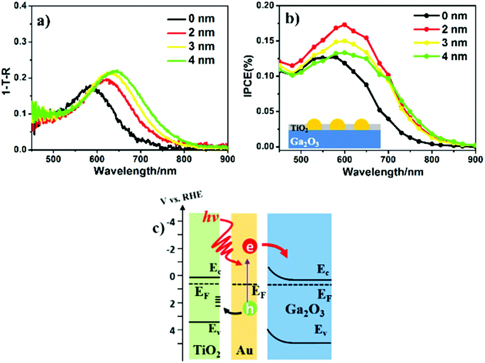 | ||
| Fig. 2 (a) Absorption spectra and (b) IPCE action spectra of Au-NPs/Ga2O3 modified with different thicknesses of TiO2. Inset: Cross-sectional schematic of TiO2/Au-NPs/Ga2O3. (c) Schematic energy diagram showing the charge transfer in TiO2/Au-NPs/Ga2O3. | ||
The photoanodes of Au-NPs/Ga2O3 with various thicknesses of the TiO2 modification layer (x-nm-TiO2/Au-NPs/Ga2O3, where x = 2–4) were investigated in the following section. The thickness of TiO2 was precisely controlled by controlling the number of ALD cycles from 40 to 80. According to the XRD measurements in Fig. S4a,† all peaks measured from 10° to 70° show almost the same diffraction angle and width, indicating the same crystallinity of Ga2O3 before and after TiO2 deposition. The bandgap (4.8 eV) of Ga2O3 estimated from the Tauc plots in Fig. S4b† kept the same before and after the deposition of TiO2. We also checked the elements oxidation states by XPS as shown in Fig. S5.† Ti 2p signal was presented after the deposition of TiO2. The new signal of Ti 2p provided the direct evidence of the TiO2 deposition on Ga2O3.26 The binding energy of O 1s peak showed slightly broadening at the lower energy side rather than peak energy shift, which is ascribed to the presence of O 1s peak of Ti–O (529.8 eV) after TiO2 deposition.27 Additionally, the binding energy and the width of Ga 2p did not change after TiO2 deposition. Based on the results above, it could be concluded that the crystallinity and band structure of Ga2O3 did not change after the deposition of TiO2. According to the top-view SEM in Fig. S7,† after the deposition of TiO2, the comparison of the morphology and particle size (dmean ∼ 15 nm) of Au-NPs before and after the deposition of the TiO2 modification layer indicated that the ALD process at 300 °C barely affected the morphology of Au-NPs on Ga2O3.
Light absorption and carrier separation are two main factors contributing to photocurrent generation. To directly study the relationship between light absorption and PEC properties, the absorption spectrum of Au-NPs was calculated as the difference between the (1 − T − R) spectrum of substrate with Au-NPs and without Au-NPs in Fig. 2a, where T and R are the transmission and reflection, respectively. Since the particle size and distribution of Au-NPs were similar, the red-shift of the peak position of the LSPR band from 585 to 645 nm was mainly caused by the refractive index increase in the surrounding media after TiO2 deposition.25 In addition, the absorption value at the LSPR peak also increased as the thickness of the TiO2 layer increased. In contrast, the absorption at wavelengths shorter than 550 nm maintained almost the same value, which was only determined by the interband transition of Au.19 The PEC performance of these modified samples is presented in Fig. 2b, and all the TiO2/Au-NPs/Ga2O3 photoelectrodes show an IPCE increase in the visible region compared with that of the Au-NPs/Ga2O3 photoelectrode. Notably, 2-nm-TiO2/Au-NPs/Ga2O3 showed the maximum IPCE value, which reached 0.17% at approximately 600 nm. Moreover, the stable photocurrent under 600 nm irradiation was approximately 1.5 times larger than that of Au-NPs/Ga2O3, as shown in Fig. S8.† The photocurrent of 2-nm-TiO2/Au-NPs/Ga2O3 also showed a good stability because the photocurrent after 7.5 hours irradiation maintained 90% of the initial value of quasi-steady photocurrent, as shown in Fig. S9.†This result indicated that the interfacial modification by TiO2 was beneficial for improving the PEC performance of Au-NPs/Ga2O3. Notably, after comparing the 2-nm-TiO2/Au-NPs/Ga2O3 and pristine Au-NPs/Ga2O3, the IPCE peak of 2-nm-TiO2/Au-NPs/Ga2O3 increased by 1.5 times, while the absorption increased by only 1.1 times at the peak LSPR wavelength. We suspect that much better charge separation occurred at the interface, resulting from the good hole-capturing ability of TiO2, which was an important factor for IPCE enhancement, as depicted in Fig. 2c. After the deposition of TiO2, the surface states of TiO2 efficiently capture the plasmon-induced holes for efficient water oxidation. Moreover, the hot electrons generated at the Au-NPs/Ga2O3 interface could be smoothly transferred to the CB of Ga2O3 due to the direct contact between Au and Ga2O3. Based on this mechanism, hot carriers should have enough energy to achieve the hot-electron injection and water oxidation. The flat-band potential of 2-nm-TiO2/Au-NPs/Ga2O3 was estimated to be −0.80 V vs. RHE after the deposition of 2 nm TiO2 as shown in Fig. S10a.† The energy barrier between the flat-band potential of Ga2O3 for hot-electron injection and the oxidation potential of water (+1.23 V vs. RHE) is estimated as 2.03 eV (610 nm). Therefore, under the irradiation of light with the wavelength of 600 nm which is the peak wavelength of the IPCE action spectrum in Fig. 2b, both hot-electron injection and water oxidation can be achieved simultaneously.
As shown in Fig. 2a and b, the redshift of the TiO2/Au-NPs/Ga2O3 IPCE peaks is not as obvious as their redshift in the absorption spectra. This observation could be explained by the threshold of photon energy needed for exciting electron/hole separation at the Au-NPs/Ga2O3 interface, as discussed in Fig. S10.† This result suggested another insight, in that the electron injected into the CB of Ga2O3 had a high negative potential energy. The energy generated under light irradiation at 600 nm on the Ga2O3 photoanode, ηphoto, was evaluated by being compared to an ideally nonpolarizable dark electrode as expressed in formula (1)
 | (1) |
The value of ηphoto is the thermodynamic energy-conversion efficiency of the photoelectrode, and the ηphoto value for 2-nm-TiO2/Au-NPs/Ga2O3 under light irradiation at 600 nm was calculated as 0.06% from the I–V characteristics shown in Fig. S11.† This value was approximately twice as large as that of the Au-NPs/TiO2-thin film (0.03%) due to the extremely negative onset potential. Therefore, the plasmonic Ga2O3 photoanode modified with the thin TiO2 layer could simultaneously achieve water oxidation and hot-electron injection with a negative reduction potential under visible light irradiation.
To further verify the hole-trapping ability of the TiO2 layer, the IPCE values of 2-nm-TiO2/Au-NPs/Ga2O3 and Au-NPs/Ga2O3 were measured in an electrolyte with triethanolamine (TEOA), as shown in Fig. 3. TEOA is a sacrificial hole scavenger due to its fast reaction kinetics based on one-electron oxidation.29 For Au-NPs/Ga2O3 without TiO2 modification, the oxidation reaction with water by holes was difficult, as discussed above. The addition of TEOA dramatically increased the oxidation reactivity even though the hole-trapping ability of the Ga2O3 surface was poor, as illustrated in Fig. S12a.† The high IPCE of 2-nm-TiO2/Au-NPs/Ga2O3 without TEOA in Fig. 3b indicated that the hot holes trapped at the surface states of 2-nm-TiO2/Au-NPs/Ga2O3 oxidized water efficiently even without the addition of TEOA, as shown in Fig. S12b.† Although the hole-trapping ability of TiO2 could improve the oxidation reactivity and charge separation, the positive effect of interfacial modification on the IPCE showed a dependence on the thickness of TiO2. When the TiO2 thickness was larger than 2 nm, the IPCE improvement decreased even though the absorption increased. To understand the PEC performance difference of TiO2/Au-NPs/Ga2O3 with different thicknesses of the TiO2 layer, the near-field distribution at the interface of TiO2/Au-NPs/Ga2O3 that determined the plasmon-induced carrier generation was calculated by a finite-difference time-domain (FDTD) simulation (Fig. 4). For Au-NPs/Ga2O3, the hot spot of the near-field was located at the interface between Au-NPs and Ga2O3, which are represented as the two bright spots in Fig. 4a. Regarding 2-nm-TiO2/Au-NPs/Ga2O3, the near-field intensity was enhanced at the three-phase boundary of TiO2/Au-NPs/Ga2O3 (Fig. 4b). However, the near-field intensity at the three-phase boundary decreased as the TiO2 thickness increased (Fig. 4c and d). Though the near-field became stronger at the interface of TiO2/Au-NPs with increasing distance from the Ga2O3 surface in Fig. 4c and d, the carriers generated at the Au-NPs/TiO2 interface and then injected into the CB of TiO2 contributed less to the IPCE, as discussed in Fig. S6.† Moreover, trapped holes at the three-phase boundary should migrate to the surface to participate in the water oxidation reaction. The thick TiO2 modification layer would also suppress hole migration to the surface because of the extended path. Consequently, 2-nm TiO2 interfacial-modified Au-NPs/Ga2O3 showed the best PEC improvement.
 | ||
| Fig. 3 IPCE action spectra of (a) Au-NPs/Ga2O3 and (b) 2-nm-TiO2/Au-NPs/Ga2O3 measured in a KClO4 aqueous solution with and without TEOA. | ||
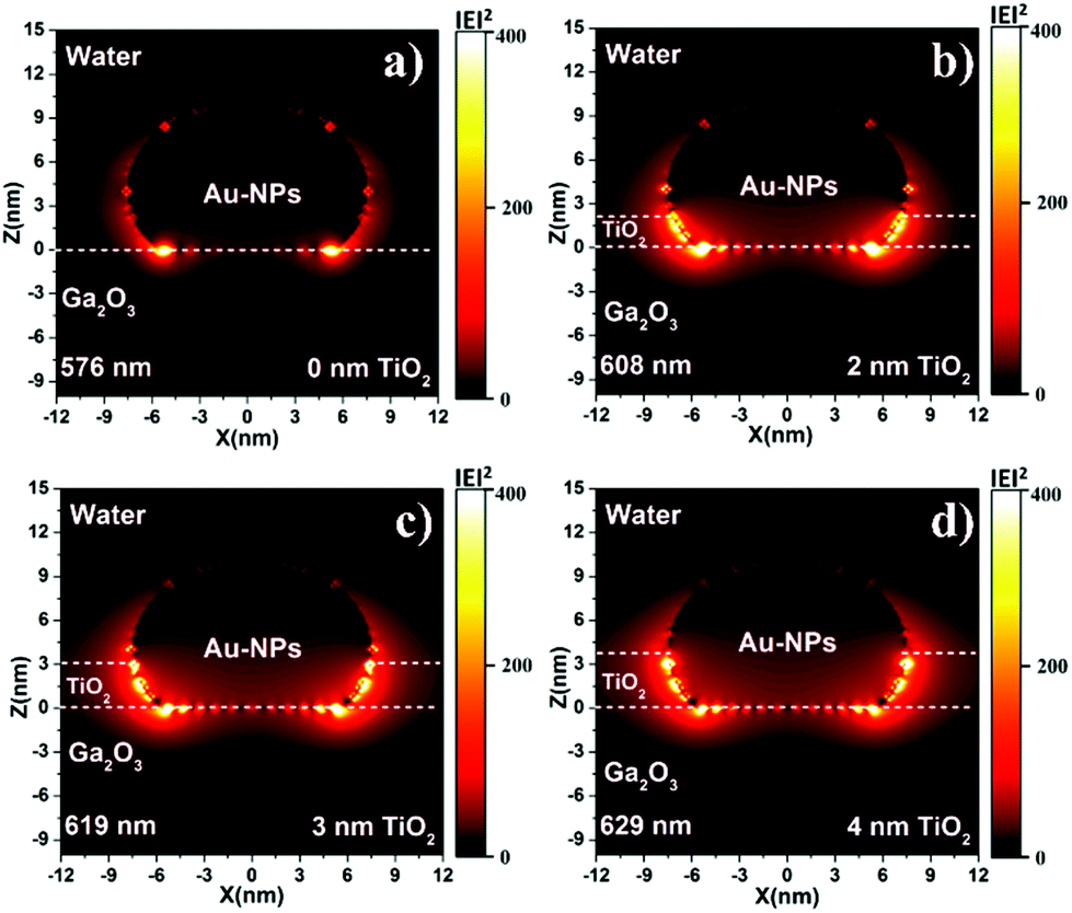 | ||
| Fig. 4 Near-field distributions of Au-NPs/Ga2O3 modified with (a) 0, (b) 2, (c) 3, and (d) 4 nm TiO2 layers, which was calculated by an FDTD simulation. | ||
Conclusions
We demonstrated plasmon-induced photocurrent generation on wide bandgap Ga2O3 under visible light irradiation. The IPCE of Au-NPs/Ga2O3 was improved by an interfacial modification consisting of the deposition of a TiO2 layer, which exhibits a high hole-trapping ability. The partial inlaying of Au-NPs with the TiO2 layer could be beneficial for trapping plasmon-induced holes at the interfacial boundary between Au-NPs and TiO2 and improving the oxidation reactivity while maintaining efficient electron transfer. The 2-nm-thick TiO2 interfacial modification shows up to a 1.5-times higher IPCE in the visible region than that without TiO2. The thermodynamic energy-conversion efficiency for the 2-nm-TiO2/Au-NPs/Ga2O3 photoelectrode under light irradiation at 600 nm was approximately twice as large as that of the Au-NPs/TiO2-thin film due to the extremely negative onset potential.Based on the above observations, the plasmonic Ga2O3 photoanode with the interfacial modification of a thin TiO2 layer could demonstrate both a high ability for reduction, such as H2 evolution, and oxidation ability for water oxidation because of the negative CB of Ga2O3 and the hole-trapping property of TiO2, respectively. We believe this interfacial modification has enormous potential for use in artificial photosynthesis and could be applied in various fields and devices for photon energy conversion through structural optimization.
Materials and methods
Sample fabrication and structure characterization
The Sn-doped single-crystal β-Ga2O3 wafer (Novel Crystal Technology, Inc.) with an orientation of (−201) was cut to a size of 9.0 × 9.0 × 0.7 mm3. These Ga2O3 substrates were successively rinsed with acetone and methanol in an ultrasonic bath for 5 min each. To fabricate Au-NPs on the surface of Ga2O3, a thin gold layer was deposited onto the substrates by electron-beam evaporation at room temperature. The deposition pressure was approximately 2.0 × 10⁻⁶ Pa, and the evaporation rate was set to approximately 0.16 Å s−1. Subsequently, the samples were annealed in air at 800 °C for 1 h. The fabrication processes are shown in Fig. S3 in the ESI.† The particle size of Au-NPs was controlled by changing the thickness of the Au film. The TiO2 layer was deposited by a commercial hot-wall flow-type ALD reactor (SUNALETM R series, Picosun, Finland) at 300 °C with a deposition rate of 0.05 nm per cycle. TiCl4 and deionized water vapor were used as the Ti and O sources, and N2 was used as the carrier gas and purge gas. The pulse time and purge time were set as 0.1 and 4.0 s, respectively. X-Ray diffraction chart was applied to check the phase structure of Ga2O3 by RIGAKU RINT-2000/PC using Cu Kα radiation. The valence of Ga, Ti and O was measured by an X-ray photoelectron spectrometer (XPS, JPS-9200, JEOL).Optical properties and morphology characterization
A photonic multichannel analyser (PMA C7473, Hamamatsu Photonics) system was applied to measure the optical reflectance and transmittance spectra. Bandgap of Ga2O3 was estimated by the Tauc plots obtained from the transmittance spectra measured by A UV-Vis spectrophotometer (UV-3100PC, SHIMADZU). The surface morphology was identified by field-emission scanning electron microscopy (FE-SEM, JSM-6700FT, JEOL) with a maximum resolution of 1 nm. Additionally, ImageJ software was used to analyse the mean particle size.Photoelectrochemical measurement
To obtain the ohmic contact, an In–Ga alloy with a weight ratio of 4![[thin space (1/6-em)]](https://www.rsc.org/images/entities/char_2009.gif) :1 was coated on the backside and sidewall of the Au-NPs/Ga2O3 substrates. Then, the samples were connected to a copper plate in a Teflon reaction cell, which was connected to an electrochemical analyser (ALS/CH Instruments 852C, ALS) with a copper lead wire. The irradiation window consisted of a pinhole with a diameter of 2.0 mm on the lid of the cell. A three-electrode system consisting of a platinum wire and a saturated calomel electrode (SCE) as the counter electrode and reference electrode, respectively, was applied to measure the PEC properties. In addition, a 0.1 M KClO4 aqueous solution without an electron donor was used as the electrolyte. During the photocurrent measurement, a potential of +0.3 V vs. SCE was applied to the working photoelectrode. The IPCE was calculated by formula (2):
:1 was coated on the backside and sidewall of the Au-NPs/Ga2O3 substrates. Then, the samples were connected to a copper plate in a Teflon reaction cell, which was connected to an electrochemical analyser (ALS/CH Instruments 852C, ALS) with a copper lead wire. The irradiation window consisted of a pinhole with a diameter of 2.0 mm on the lid of the cell. A three-electrode system consisting of a platinum wire and a saturated calomel electrode (SCE) as the counter electrode and reference electrode, respectively, was applied to measure the PEC properties. In addition, a 0.1 M KClO4 aqueous solution without an electron donor was used as the electrolyte. During the photocurrent measurement, a potential of +0.3 V vs. SCE was applied to the working photoelectrode. The IPCE was calculated by formula (2): | (2) |
Numerical simulations
Full-field electromagnetic wave simulations were performed using the FDTD method (FDTD Solutions, Lumerical). The investigated structure was simulated using perfectly matched layers along the z-direction and periodic boundary conditions along the x-and y-directions with a period of 20 nm. An ellipsoid sphere with a diameter of 15 nm in the x and y directions and 10 nm in the z direction was used to model the Au-NPs. In the simulation, the refractive index of Au was taken from the optical constants of Johnson and Christy. Ga2O3 and TiO2 were treated as dielectric materials with refractive indices of 1.8 and 2.4, respectively.Conflicts of interest
There are no conflicts to declare.Acknowledgements
We acknowledge financial support from JSPS KAKENHI (Grant No. JP18H05205, JP18K05053, JP19H02737, JP19H04667, JP20H05083, and JP20K15113), the Nanotechnology Platform (Hokkaido University), and the Dynamic Alliance for Open Innovation Bridging Human, Environment and Materials (Five-Star Alliance) of MEXT.Notes and references
- L. Ni, M. Tanabe and H. Irie, Chem. Commun., 2013, 49, 10094–10096 RSC.
- K. Maeda and K. Domen, J. Phys. Chem. C, 2007, 111, 7851–7861 CrossRef CAS.
- M. Navarrete, S. Cipagauta-Díaz and R. Gómez, J. Chem. Technol. Biotechnol., 2019, 94, 3457–3465 CrossRef CAS.
- Y. Sakata, Y. Matsuda, T. Nakagawa, R. Yasunaga, H. Imamura and K. Teramura, ChemSusChem, 2011, 4, 181–184 CAS.
- Y. Sakata, T. Nakagawa, Y. Nagamatsu, Y. Matsuda, R. Yasunaga, E. Nakao and H. Imamura, J. Catal., 2014, 310, 45–50 CrossRef CAS.
- Y. Hou, X. Wang, L. Wu, Z. Ding and X. Fu, Environ. Sci. Technol., 2006, 40, 5799–5803 CrossRef CAS.
- H. Tsuneoka, K. Teramura, T. Shishido and T. Tanaka, J. Phys. Chem. C, 2010, 114, 8892–8898 CrossRef CAS.
- T. Oshima, K. Kaminaga, H. Mashiko, A. Mukai, K. Sasaki, T. Masui, A. Kuramata, S. Yamakoshi and A. Ohtomo, Jpn. J. Appl. Phys., 2013, 52 Search PubMed.
- A. Kudo and I. Mikami, J. Chem. Soc., Faraday Trans., 1998, 94, 2929–2932 RSC.
- H. Kong, H. Li, G. Lin and H. Zhang, Catal. Lett., 2011, 141, 886–894 CrossRef CAS.
- Y. Sakata, Y. Matsuda, T. Yanagida, K. Hirata, H. Imamura and K. Teramura, Catal. Lett., 2008, 125, 22–26 CrossRef CAS.
- T. Yanagida, Y. Sakata and H. Imamura, Chem. Lett., 2004, 33, 726–727 CrossRef CAS.
- X. Shi, K. Ueno, T. Oshikiri and H. Misawa, J. Phys. Chem. C, 2013, 117, 24733–24739 CrossRef CAS.
- Z. Zheng, W. Xie, B. Huang and Y. Dai, Chem. – Eur. J., 2018, 24, 18322–18333 CrossRef CAS.
- A. Abdalla, I. Khan, M. Sohail and A. Qurashi, Sol. Energy, 2019, 181, 333–338 CrossRef CAS.
- X. Ma, Y. Dai, L. Yu and B. Huang, Light: Sci. Appl., 2016, 5, e16017 CrossRef CAS.
- K. Wu, J. Chen, J. McBride and T. Lian, Science, 2015, 349, 632–635 CrossRef CAS.
- C. Clavero, Nat. Photonics, 2014, 8, 95–103 CrossRef CAS.
- X. Shi, K. Ueno, T. Oshikiri, Q. Sun, K. Sasaki and H. Misawa, Nat. Nanotechnol., 2018, 13, 953–958 CrossRef CAS.
- X. Shi, X. Li, T. Toda, T. Oshikiri, K. Ueno, K. Suzuki, K. Murakoshi and H. Misawa, ACS Appl. Energy Mater., 2020, 3, 5675–5683 CrossRef CAS.
- K. Suzuki, X. Li, Y. Wang, F. Nagasawa and K. Murakoshi, ACS Energy Lett., 2020, 5, 1252–1259 CrossRef CAS.
- S. Bera, J. Lee, S. Rawal and W. Lee, Appl. Catal., B, 2016, 199, 55–63 CrossRef CAS.
- P. Reineck, D. Brick, P. Mulvaney and U. Bach, J. Phys. Chem. Lett., 2016, 7, 4137–4141 CrossRef CAS.
- R. Sundararaman, P. Narang, A. Jermyn, W. Goddard and H. Atwater, Nat. Commun., 2014, 5, 5788 CrossRef CAS.
- C. Sonnichsen, T. Franzl, T. Wilk, G. von Plessen, J. Feldmann, O. Wilson and P. Mulvaney, Phys. Rev. Lett., 2002, 88, 077402 CrossRef CAS.
- M. Warwick, G. Carraro, E. Toniato, A. Gasparotto and C. Maccato, Surf. Sci. Spectra, 2016, 23, 61–69 CrossRef CAS.
- B. Bharti, S. Kumar, H. Lee and R. Kumar, Sci. Rep., 2016, 6, 323 Search PubMed.
- R. Coridan, A. Nielander, S. Francis, M. McDowell, V. Dix, S. Chatman and N. Lewis, Energy Environ. Sci., 2015, 8, 2886–2901 RSC.
- Y. Pellegrin and F. Odobel, C. R. Chim., 2017, 20, 283–295 CrossRef CAS.
Footnote |
| † Electronic supplementary information (ESI) available: Description of fabrication schematic. Morphology of Au-NPs. Near-field spectrum of different size of Au-NPs. I–V, I–t and Mott–Schottky curves. Schematic of charge transfer. See DOI: 10.1039/d0nr06319c |
| This journal is © The Royal Society of Chemistry 2020 |