
 Open Access Article
 This Open Access Article is licensed under a Creative Commons Attribution-Non Commercial 3.0 Unported Licence
Heterotwin Zn3P2 superlattice nanowires: the role of indium insertion in the superlattice formation mechanism and their optical properties†
Simon
Escobar Steinvall‡
 a,
Lea
Ghisalberti‡
a,
Reza R.
Zamani‡
b,
Nicolas
Tappy
a,
Fredrik S.
Hage
cd,
Elias Z.
Stutz
a,
Mahdi
Zamani
a,
Rajrupa
Paul
a,
Jean-Baptiste
Leran
a,
Quentin M.
Ramasse
ce,
W.
Craig Carter
af and
Anna
Fontcuberta i Morral
*ag
a,
Lea
Ghisalberti‡
a,
Reza R.
Zamani‡
b,
Nicolas
Tappy
a,
Fredrik S.
Hage
cd,
Elias Z.
Stutz
a,
Mahdi
Zamani
a,
Rajrupa
Paul
a,
Jean-Baptiste
Leran
a,
Quentin M.
Ramasse
ce,
W.
Craig Carter
af and
Anna
Fontcuberta i Morral
*ag
aLaboratory of Semiconductor Materials, Institute of Materials École Polytechnique Fédérale de Lausanne, 1015 Lausanne, Switzerland
bCentre Interdisciplinaire de Microscopie Électronique, École Polytechnique Fédérale de Lausanne, 1015 Lausanne, Switzerland
cSuperSTEM Laboratory, SciTech Daresbury Campus, Keckwick Lane, Warrington WA4AD, UK
dDepartment of Materials, University of Oxford, Oxford, OX1 3PH, UK
eSchool of Chemical and Process Engineering and School of Physics and Astronomy, University of Leeds, Leeds LS2 9JT, UK
fDepartment of Materials Science and Engineering, Massachusetts Institute of Technology, Cambridge, Massachusetts 02139, USA
gInstitute of Physics, École Polytechnique Fédérale de Lausanne, 1015 Lausanne, Switzerland. E-mail: anna.fontcuberta-morral@epfl.ch
First published on 22nd October 2020
Abstract
Zinc phosphide (Zn3P2) nanowires constitute prospective building blocks for next generation solar cells due to the combination of suitable optoelectronic properties and an abundance of the constituting elements in the Earth's crust. The generation of periodic superstructures along the nanowire axis could provide an additional mechanism to tune their functional properties. Here we present the vapour–liquid–solid growth of zinc phosphide superlattices driven by periodic heterotwins. This uncommon planar defect involves the exchange of Zn by In at the twinning boundary. We find that the zigzag superlattice formation is driven by reduction of the total surface energy of the liquid droplet. The chemical variation across the heterotwin does not affect the homogeneity of the optical properties, as measured by cathodoluminescence. The basic understanding provided here brings new propsects on the use of II–V semiconductors in nanowire technology.
Introduction
Filamentary crystals, also known as nanowires, have provided additional design freedom in the elaboration of materials with desirable properties.1–4 This arises from the possibility of engineering the crystal phase and material composition, and for the possibility of expanding the structure in three dimensions.3,5,6 Among the design opportunities, the composition or structure of nanowires can be arranged periodically in the form of superlattices.6–9 The periodicity of the superstructure modulates both the electronic and phonon (vibrational) states, depending on the magnitude of the period.10–13 Semiconductor superlattices find applications in the optoelectronic and thermoelectric arena.14–17 In thin films, the materials combinations are mostly restrained due to lattice-mismatch and thermal expansion conditions. Superlattice nanowire structures circumvent these limitations, and have been achieved by modulating the composition, crystal phase, and crystal orientation through rotational twins.5–8Twin superlattices (TSLs) in semiconductors were predicted by Ikonic et al. in 1993.18 More recently, they were implemented in nanowire form, first in Al2O3 and ZnSe, and subsequently in InP.19–21 These TSLs have been obtained mainly by the vapour–liquid–solid (VLS) method in which a nanoscale liquid droplet preferentially collects the growth precursors.22 In addition to a periodic arrangement of twins, these nanowire superlattices adopt a characteristic zigzag morphology with alternating (111)A/B facets in the case of zinc blende nanowires.7,8 According to Algra et al., twin formation is determined by energy minimisation involving the stability of the droplet and the surface energy of the facets as a function of their polarity -(111) a or B-.8
Zinc phosphide, Zn3P2, has recently attracted attention as a compound semiconductor made of elements that are abundant in the Earth's crust with optoelectronic properties suitable for photovoltaic applications.23–28 Zn3P2 has been obtained both in the form of bulk crystals,29,30 thin films,25,26,31 and nanostructures.9,24,32–34 Zinc phosphide based solar cells with an efficiency of up to 6% have been eported.30 This value is still well below the theoretical limit (>30%), illustrating the improvement potential of this material.35,36
The synthesis of Zn3P2 nanowires can follow the VLS and the vapour–solid mechanisms, with In, Sn, and Au as catalysts.9,24,32–34,37,38 Zn3P2 nanowires adopt various morphologies depending on the fabrication method and/or growth conditions, including a zigzag superlattice.9,24,32–34 In contrast with III–V compound semiconductors, Zn3P2 exhibits a centrosymmetric tetragonal structure, and thus also non-polar facets and main crystal symmetry directions.29 Consequently, all side facets of Zn3P2 zigzag nanowires are always Zn-terminated.27,33 This means that the mechanism through which Zn3P2 obtains a zigzag morphology is inconsistent with the model proposed based on III–Vs.8
In this paper we reveal the nature of the defects leading to the zigzag structure using aberration-corrected and analytical scanning transmission electron microscopy (STEM). In addition, we explain the formation mechanisms based on simulations of the surface energetics of the droplet as a function of the nanowire cross-section. Finally, we outline the consequences of this periodic structure for the optical functionality through cathodoluminescence spectroscopy (CL).
Experimental
The Zn3P2 nanowires were epitaxially grown in a Veeco GENxplor molecular beam epitaxy (MBE) system on InP (100) substrates. They were grown through In catalysed VLS, with the In originating from the substrate.24 The analysed samples were grown at a manipulator temperature of 250 °C and a V/II ratio of 1.15 or 1.45 for four hours, with additional details on the growth in ref. 24. The nanowires were transferred to copper TEM grids with holey carbon by scraping the grid on the growth substrate for TEM studies, and were used as grown for CL studies.Scanning electron microscopy (SEM) images were acquired using a Zeiss Merlin FE-SEM equipped with a Gemini column. The operating conditions were an acceleration voltage of 3 kV and a beam current of 100 pA. An in-lens secondary electron detector was used for the imaging.
Droplet simulations were performed using the Surface Evolver software,39 which computes minimised surface energy by optimising shapes given constraints and wetting angles. We implement the interfacial energy of the liquid–solid interface by means of the Young's equation with a contact angle of 43° when the triple line is unconstrained. The vertical axis in Fig. 2c is the total energy divided by L2, with L being the average length of the sides, and the difference between the solid–liquid and the solid surface tensions. The average length of the side remains constant with a value of 1.57. Regarding the geometrical constraint, the triple line is not pinned to the edge, but is left free to move inside the polygon. To build the polygon, centred at the origin, we define an equation for each side of the hexagon through the lat and shrink parameters, illustrated in the ESI.† While the lat parameter is fixed at 0.55 and defines the apothem of the reference hexagon, the shrink parameter is variable controlling the shape of the constraint since it represents the normal between the facet centroid and the selected facet. By varying the shrink parameter from −0.25 to 0.25, we can reproduce the evolution of the nanowire cross-section from left oriented triangle to right oriented triangle (HT1 & HT2), passing through the hexagonal geometry at shrink equal to 0. To compare the effect of the volume we performed the simulations for three different droplet volumes: 0.125, 0.225, and 0.325 with dimensions of L3.
Aberration-corrected bright-field/high-angle annular dark-field (BF/HAADF) STEM images and electron energy loss spectroscopy (EELS) maps were collected on a STEM-dedicated Nion microscope (US100MC) operating at 60 kV. The Nion UltraSTEM 100MC HERMES is equipped with a C5 Nion probe corrector (full correction up to 6-fold astigmatism C5, 6) and a UHV Gatan Enfinium ERS spectrometer optimised for high energy resolution with high-stability electronics. The microscope is equipped with a cold-field emission gun (C-FEG), having an energy spread of 0.35 eV. The beam convergence semi-angle was 31.5 mrad and the EEL spectrometer entrance aperture semi-angle was 44 mrad. Image detector angles were 0–14 mrad (BF) and 100–230 mrad (HAADF). To minimise contamination, the specimens were baked prior to insertion at 130 °C in vacuum (∼10−6 Torr), and the microscope column is maintained at ultrahigh vacuum (UHV). The denoising of STEM-EELS datasets was done using the MSA plugin for Gatan's Digital Micrograph suite, commercially available from HREM research.40 Example spectra are shown in the ESI,† and the 443 eV and 1020 eV peaks were used for EEL mapping of In and Zn, respectively. Further imaging was also performed in a FEI Titan Themis 60–300 kV TEM operating at 200 or 300 kV. The machine is equipped with a field emission gun (X-FEG), a monochromators, two aberration correctors (one pre-specimen probe-corrector, and one post-specimen image corrector), and a Fischione HAADF detector. The collection angles are typically 85–200 mrad for HAADF-STEM images. The BF and HAADF images were denoised using radial a Weiner filter. Viewing direction illustrations were created in Mathematica.
An Attolight Rosa setup equipped with an Andor Newton 920 Si-CCD was used for CL measurements. It was operated at room temperature with an acceleration voltage of 3 kV, a beam current of <1 nA, and an exposure time of 50 ms per pixel. The nanowires were mounted on a stage with 20° tilt. Denoising of the hyperspectral maps was done through principal-component analysis (PCA) using the Hyperspy Software.41 Peak fitting was done after data treatment based on the approach described in ref. 42.
Results and discussion
Electron microscopy
Fig. 1a shows a representative secondary electron SEM images of a typical zigzag Zn3P2 nanowire. These nanowires grow perpendicular to (101) with side facets belonging to {101}.24,33 While the lateral facets in III–V superlattices, (111)A and (111)B, can exhibit different polarities, this is not the case for Zn3P2 (101) facets as they are all Zn-terminated.7,8,27 The supposed difference between the lateral facets has been cited as one of the driving forces for the formation of TSL nanowires. This argument cannot be applied to this case as Zn3P2 does not display polar facets. Before discussing the mechanism, we disclose the nature of the interface dividing the zigzag regions in the nanowire.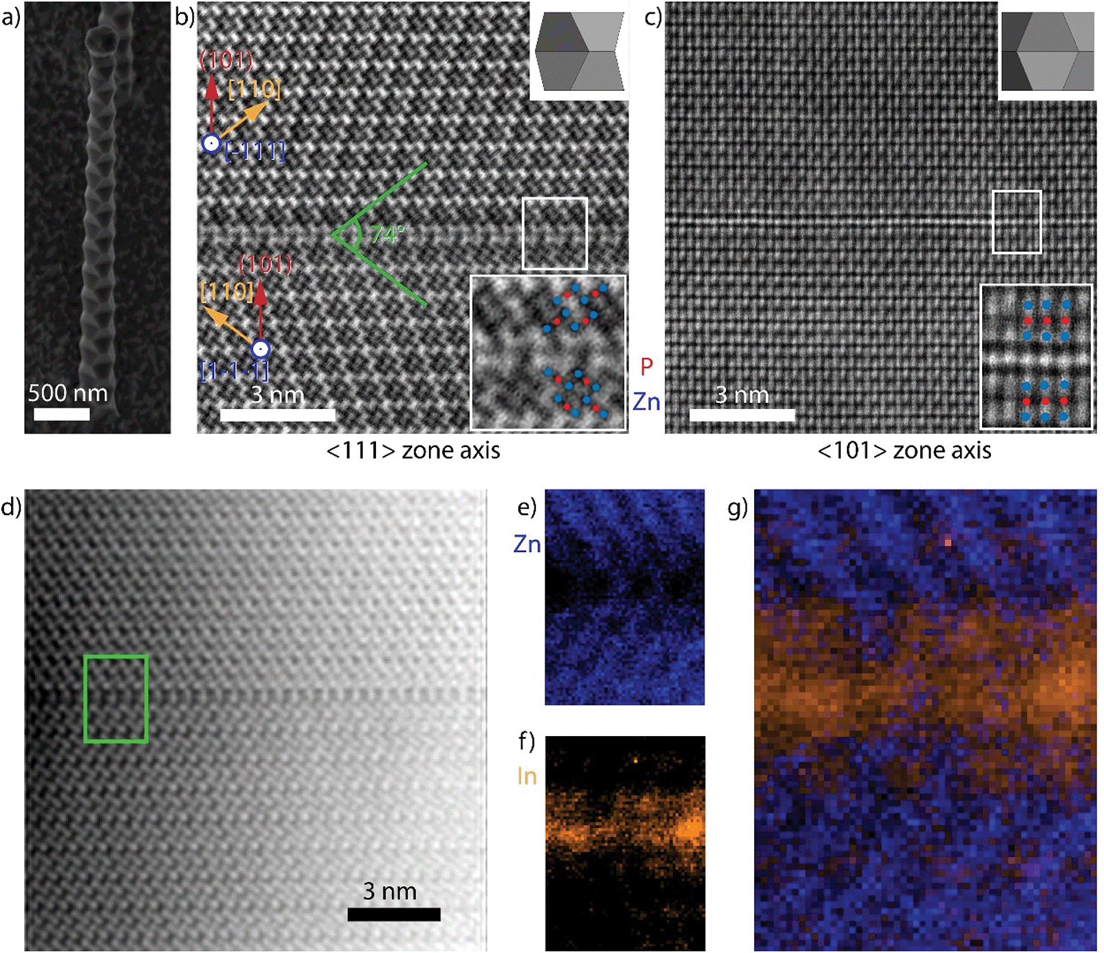 | ||
| Fig. 1 (a) Secondary electron SEM image of a superlattice nanowire. (b) Aberration corrected BF-STEM image taken along a [111] zone axis in the region around the zigzag interface with an inset illustrating the viewing direction. (c) Aberration corrected HAADF-STEM image taken along a [101] zone axis in the region around the zigzag interface. The top inset illustrates the viewing direction and the bottom inset displays a “close up” on the interface. (d) HAADF-STEM image ([111] zone axis) of the region where the EELS maps were acquired (green). (e–g) Core-loss EELS maps of Zn (blue – e), In (orange – f), and the combination (g), showing the localised presence of In in the region around the stacking fault. | ||
Fig. 1b shows an aberration-corrected BF-STEM image of a zigzag nanowire ([111] zone axis), revealing a “twin-like” planar defect separating different segments that are mirrored. This structural defect is akin to the twin planes in the III–V TSL nanowires: it interfaces two segments of the nanowire that appear to be rotated 180° around the nanowire growth axis -the (101) plane-, which is the most common twin plane in tetragonal systems.43 Here we observe a (224) planar spacing of 1.97 ± 0.07 Å, which is within experimental error of the literature value of 2.024 Å.29
Fig. 1c shows the HAADF-STEM image of a region equivalent to that shown in Fig. 1b, viewed along the other major zone axis, [−101]. The bottom insets corresponds to “close ups” of the interfaces, identifying sets of trimers (Zn – blue, P – red) at each side of the defect. The topmost insets show a three-dimensional model of the structure, highlighting the viewing direction of the respective zone axes. While the defect is easily discerned by the increase in intensity and break in periodicity in Fig. 1c, the structure is not perfectly mirrored along this zone axis. Instead, we observe a translation of the top crystal by a (400) plane along the 〈100〉 direction perpendicular to the zone axis. Furthermore, as corroborated below, the interfacial defect extends to more than one monolayer, and is of a different composition than the neighbouring segments. Thus, the two rotated crystals are separated, not sharing any crystal lattice points, and consequently this defect cannot be considered a standard twin.
We not turn to the study of the nature of the interface separating the twinned regions by providing data on the chemical composition. For this, we took the core-loss EELS of the “twin” and the adjacent regions – marked with a green square in Fig. 1d, resulting in chemical maps with atomic-scale resolution.44,45Fig. 1e–g display the resulting chemical mapping of Zn (blue – e), In (orange – f), and combined (g). P mapping did not provide the same resolution, and a constant signal was observed throughout. The maps reveal the presence of In at the interface and the neighbouring layers, accompanied by a drop in the Zn content. The presence of In is consistent with the intensity analysis in the HAADF-STEM images, especially from the [−101] direction (Fig. 1c). The interface there appears slightly brighter than the rest, suggesting the presence of a heavier element, i.e. In. Given the chemical inhomogeneity across the boundary, the defect should rather be identified as a heterotwin.46 The In originates from the droplet that drives the VLS growth,24 which was in contact with the twin region during formation.
The utilisation of a chemical heterogeneity at the boundaries or planar defects have been reported in Al/TiN composites and in doped II–VI compounds such as ZnO. In the case of Al, N-terminated TiN lowers the formation energy of twins, and they provide significantly improved mechanical properties.46,47 In ZnO, trivalent metals such as Al, Fe, Ga, or In have shown to precipitate at the interface of inversion domain boundaries.48 The presence of trivalent metals in II–VI defects modifies the bonding coordination from four in a tetrahedral fashion to eight in an octahedral one, causing the polarity inversion.49–52 However, in the case considered here the defect cannot be classified as an inversion domain boundary as there is no polarity inversion associated with it. In the following section we discuss the mechanism by which Zn3P2 forms a zigzag structure via a heterotwin.
Zigzag mechanism
To investigate the driving forces prompting the regular insertion of heterotwins, we analysed the heterotwin periodicity along the nanowire length, x (nm), and as a function of W, an approximation of the cross-sectional apothem. The trend was observed in multiple nanowires, while the equation is based on the high-resolution TEM image shown in Fig. S3.† Similar to III–V TSL nanowires, the heterotwin periodicity in Zn3P2 nanowires depends on their diameter.7,53 The zigzag morphology results in the width being a periodic function with an amplitude with linear decay: | (1) |
Regarding possible explanations for the heterotwin formation mechanism, previous studies argued that twins in a zigzag structure form to minimise the nanowire surface energy.8,54 The argument is reasonable for compound semiconductor nanowires exhibiting facets with different polarities and thus different surface energies. However, Zn3P2 is not polar. The basic structural unit consists of symmetric Zn–P–Zn trimers, instead of asymmetric cation–anion dumbbells such as In–P in InP, and its centrosymmetric crystal structure.29,48,55 Thus, all facets in the zigzag structure are equivalent.27 This means we cannot reasonably attribute the instigation of the Zn3P2 twinning process to nanowire surface energy minimisation alone. As discussed below, deformation of the liquid droplet during growth provides a more compelling argument.
We studied the droplet stability as a function of the volume and underlying cross-section of the nanowire, which varies during the zigzag formation as depicted in Fig. 2a and b. To this end, we computed the surface energy of the liquid droplet and the interface with the nanowire using the finite-element based software Surface Evolver.39 We used a Young angle of 43°, which is the experimental value found ex situ.56 Young's angles differing from 43° do not change the conclusion regarding alternating stability, the only modify the threshold for heterotwin formation.
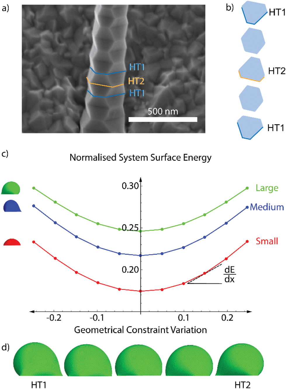 | ||
| Fig. 2 (a) Secondary electron SEM image of a zigzag Zn3P2 nanowire (b) schematic of the development of the cross-section of the nanowire as a function of the nanowire's growth axis, (c) results of the computation of the system (droplet and nanowires top facet) normalised surface energy (normalisation explained in the text) as a function of the variation of the geometry of the NW's top facet for three different referential droplet volume: small (red), medium (blue) and large (green); (d) 3D sketch of the large droplet morphology upon the zigzag period. | ||
Fig. 2c illustrates the evolution of the surface energy of the droplet plus the liquid–solid interface during one zigzag cycle. We include the curves for three relative values of droplet volumes, which all follow a similar trend. The total surface energy has been normalised by the average length of the sides, constant throughout all simulations, by the surface energy of a floating sphere with an identical volume, and by the surface tension of the liquid–vapour interface. Due to the pinning of the liquid at the edge of the faceted nanowires, an increase in the liquid volume results in the increase of the apparent contact angle.56 The normalised surface energy increases with the liquid volume due to the expansion and deformation of the liquid surface at the edges. The lowest normalised surface energy corresponds to the configuration with hexagonal nanowire cross-section, where the droplet is the least deformed. The normalised surface energy increases parabolically (to a second order approximation) with the modification of the liquid–solid interface area. The slope of the curve increases with the droplet deformation. A representative display of the predicted droplet shape during the zigzag process is shown in Fig. 2d. It shows that the deformation is larger at the corners of the cross-section. In addition, the local and overall deformations are the largest when the cross-section is the closest to a triangular shape. This increasing deformation with the deviation from a hexagonal cross-section explains the increase in the normalised surface energy.
The introduction of a heterotwin constitutes a mechanism to stop the increase in surface energy during the nanowire elongation caused by the droplet's deformation.53,57 As the energy required to form a heterotwin (EHT) is fixed, there is a critical geometry of the nanowire's cross-section after which it is energetically favourable to insert a heterotwin rather than to continue increasing the total normalised surface energy. The probability of creating a heterotwin along the nanowire axis, P(x), should thus increase with the normalised surface energy of the system, γ(x), as:

After formation of a heterotwin, the normalised surface energy decreases with nanowire elongation due to the change in the facet orientation and return towards a hexagonal cross section.
Optical properties
Previous studies on Zn3P2 indicate that it exhibits a direct bandgap at ∼1.5 eV, which is close to the ideal bandgap for the highest efficiency of single junction solar cells.58 In our recent work, we demonstrated that zigzag Zn3P2 nanowires luminesce at 1.43 eV at cryogenic temperatures, which is relatively close to the expected value of the bandgap.24 We have observed that in Zn3P2 nanowires with a square cross-section, luminescence can vary with the relative stoichiometry between the Zn and P.24 Given the composition variation at the heterotwin in the zigzag nanowires, the question arises of whether the optical properties vary at these points. To ascertain their potential influence, we performed CL on zigzag nanowires at room temperature. The experimental conditions were chosen as to decrease the diffusion length and allow for higher spatial resolution measurements compared to previous studies.Fig. 3a shows a panchromatic map of the CL emission. We observe a ∼10% variation in the emission intensity around edges and on the outward facet orientation compared to that of the inward orientation of the zigzag structure. We attribute this fluctuation to the variations in electron-beam excitation as a function of the morphology (see ESI† for more details). Detailed spectra along one oscillation of the zigzag morphology indicated by the arrow in Fig. 3a are shown in Fig. 3b. We observe to main peaks centred around 869 and 950 nm (1.43 eV and 1.30 eV, respectively), which correspond to sub-bandgap emission, potentially caused by the incorporation of indium in the bulk.59 First principle simulations should be performed to confirm this hypothesis. We also distinguish a third weaker peak centred around 748 nm (1.66 eV). This peak could correspond to emission from the Γ2 transition 260 meV above the bandgap, available due to the high energy excitation of CL.58,60 The spectra along and on each side of the heterotwin are qualitatively extremely similar. The similarity of the spectra along the zigzag structure could be due to the carrier diffusion length being larger than the excitation volume.58 The spectra intensity tends to decrease down the nanowire axis. We attribute this to optical wave-guiding effects. The channelling of CL signal between optical modes of a nanowire depends strongly on the excitation position.61 In the measurement geometry used here, and with the restricted collection angle of the CL setup, the signal can be collected only when emitted from the top of the wire and for a restricted range of angles. This would explain the peak intensity variations on a λ/2 spatial scale as observed in Fig. 3. One would require angle-resolved CL experiments to confirm this.
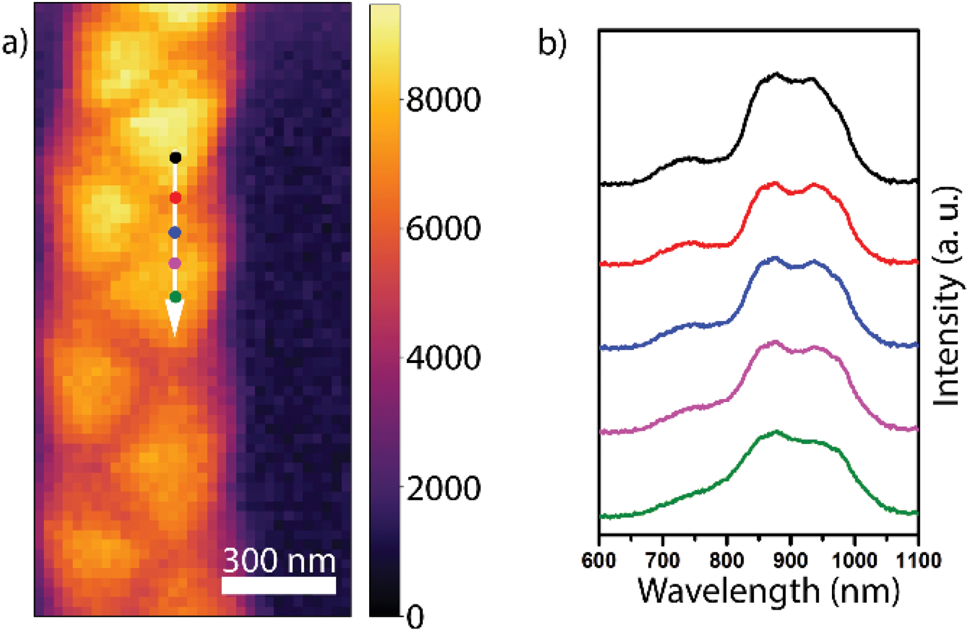 | ||
| Fig. 3 (a) High-resolution panchromatic CL intensity map of a zigzag nanowire with the white arrow indicating the linescan of the extracted spectra in (b), of which the second and fourth from the top were extracted from regions on top of the heterotwin. | ||
Conclusions
In conclusion, we have demonstrated that the Zn3P2 superlattice nanowires do not form through regular twinning, as observed in their III–V analogue. Instead, an In-rich heterotwin is formed, as shown through EELS mapping and aberration-corrected STEM imaging, which facilitates the rotation of the crystal structure between segments through the inset of a separate material. Furthermore, we developed a model to explain the onset of heterotwin formation. Based on the non-polar nature of Zn3P2 we could tie the model solely to the constraints posed by the droplet shape as a function of the nanowire cross-section. Characterisation of the emission through room temperature CL shows no effect of the heterotwins on the functional properties.Conflicts of interest
There are no conflicts to declare.Acknowledgements
S. E. S., E. S., M. Z., R. P., J. L., and A. F. i M. were supported by the SNSF Consolidator grant BSCGI0-157705. N. T. and A. F. i M. were supported by SNSF grant 20B2-1 17668. L. G., W. C. C., and A. F. i M. were supported by SNSF via project 200021_169908 and SCR0222237. R. R. Z. was supported by EPFL-CIME. F. S. H., Q. M. R., and the SuperSTEM Laboratory, the U. K. National Research Facility for Advanced Electron Microscopy, were supported by the Engineering and Physical Sciences Research Council (EPSRC).Notes and references
- J. Arbiol, M. de la Mata, M. Eickhoff and A. F. i Morral, Mater. Today, 2013, 16, 213–219 CrossRef CAS.
- P. C. McIntyre and A. Fontcuberta i Morral, Mater. Today Nano, 2020, 9, 100058 CrossRef.
- K. A. Dick, K. Deppert, M. W. Larsson, T. Mårtensson, W. Seifert, L. R. Wallenberg and L. Samuelson, Nat. Mater., 2004, 3, 380–384 CrossRef CAS.
- L. Güniat, P. Caroff and A. Fontcuberta i Morral, Chem. Rev., 2019, 119, 8958–8971 CrossRef.
- M. S. Gudiksen, L. J. Lauhon, J. Wang, D. C. Smith and C. M. Lieber, Nature, 2002, 415, 617–620 CrossRef CAS.
- K. A. Dick, C. Thelander, L. Samuelson and P. Caroff, Nano Lett., 2010, 10, 3494–3499 CrossRef CAS.
- P. Caroff, K. A. Dick, J. Johansson, M. E. Messing, K. Deppert and L. Samuelson, Nat. Nanotechnol., 2009, 4, 50–55 CrossRef CAS.
- R. E. Algra, M. A. Verheijen, M. T. Borgstrom, L.-F. Feiner, G. Immink, W. J. P. van Enckevort, E. Vlieg and E. P. A. M. Bakkers, Nature, 2008, 456, 369–372 CrossRef CAS.
- G. Shen, P.-C. Chen, Y. Bando, D. Golberg and C. Zhou, J. Phys. Chem. C, 2008, 112, 16405–16410 CrossRef CAS.
- D. Spirkoska, J. Arbiol, A. Gustafsson, S. Conesa-Boj, F. Glas, I. Zardo, M. Heigoldt, M. H. Gass, A. L. Bleloch, S. Estrade, M. Kaniber, J. Rossler, F. Peiro, J. R. Morante, G. Abstreiter, L. Samuelson and A. Fontcuberta i Morral, Phys. Rev. B: Condens. Matter Mater. Phys., 2009, 80, 245325 CrossRef.
- M. De Luca, C. Fasolato, M. A. Verheijen, Y. Ren, M. Y. Swinkels, S. Kölling, E. P. A. M. Bakkers, R. Rurali, X. Cartoixà and I. Zardo, Nano Lett., 2019, 19, 4702–4711 CrossRef CAS.
- Z. Ikonic, G. P. Srivastava and J. C. Inkson, Phys. Rev. B: Condens. Matter Mater. Phys., 1995, 52, 14078–14085 CrossRef CAS.
- Z. Ikonic, G. P. Srivastava and J. C. Inkson, Phys. Rev. B: Condens. Matter Mater. Phys., 1993, 48, 17181–17193 CrossRef CAS.
- M. Y. Swinkels and I. Zardo, J. Phys. D, 2018, 51, 353001 CrossRef.
- N. Guan, X. Dai, A. V. Babichev, F. H. Julien and M. Tchernycheva, Chem. Sci., 2017, 8, 7904–7911 RSC.
- P. Krogstrup, H. I. Jørgensen, M. Heiss, O. Demichel, J. V. Holm, M. Aagesen, J. Nygard and A. Fontcuberta i Morral, Nat. Photonics, 2013, 7, 306–310 CrossRef CAS.
- S. A. Mann, R. R. Grote, R. M. Osgood Jr., A. Alu and E. C. Garneet, ACS Nano, 2016, 10, 8620–8631 CrossRef CAS.
- Z. Ikonic, G. P. Srivastava and J. C. Inkson, Solid State Commun., 1993, 86, 799–802 CrossRef CAS.
- X.-S. Fang, C.-H. Ye, L.-D. Zhang and T. Xie, Adv. Mater., 2005, 17, 1661–1665 CrossRef CAS.
- Q. Li, X. Gong, C. Wang, J. Wang, K. Ip and S. Hark, Adv. Mater., 2004, 16, 1436–1440 CrossRef CAS.
- G. Shen, Y. Bando, B. Liu, C. Tang and D. Golberg, J. Phys. Chem. B, 2006, 110, 20129–20132 CrossRef CAS.
- R. Wagner and W. Ellis, Appl. Phys. Lett., 1964, 4, 89–90 CrossRef CAS.
- R. Katsube and Y. Nose, J. Solid State Chem., 2019, 280, 120983 CrossRef CAS.
- S. Escobar Steinvall, N. Tappy, M. Ghasemi, R. R. Zamani, T. LaGrange, E. Z. Stutz, J.-B. Leran, M. Zamani, R. Paul and A. Fontcuberta i Morral, Nanoscale Horiz., 2020, 5, 274–282 RSC.
- J. P. Bosco, G. M. Kimball, N. S. Lewis and H. A. Atwater, J. Cryst. Growth, 2013, 363, 205–210 CrossRef CAS.
- R. Paul, N. Humblot, S. Escobar Steinvall, E. Z. Stutz, S. S. Joglekar, J.-B. Leran, M. Zamani, C. Cayron, R. Logé, A. G. del Aguila, Q. Xiong and A. Fontcuberta i Morral, Cryst. Growth Des., 2020, 20, 3816–3825 CrossRef CAS.
- N. Y. Dzade, Phys. Chem. Chem. Phys., 2020, 22, 1444–1456 RSC.
- M. Y. Swinkels, A. Campo, D. Vakulov, W. Kim, L. Gagliano, S. Escobar Steinvall, H. Detz, M. De Luca, A. Lugstein, E. P. A. M. Bakkers, A. Fontcuberta i Morral and I. Zardo, Phys. Rev. Appl., 2020, 14, 024045 CrossRef CAS.
- M. V. Stackelberg and R. Paulus, Z. Phys. Chem., 1935, 28, 427–460 Search PubMed.
- M. Bhushan and A. Catalano, Appl. Phys. Lett., 1981, 38, 39–41 CrossRef CAS.
- T. Suda, K. Kakishita, H. Sato and K. Sasaki, Appl. Phys. Lett., 1996, 69, 2426–2428 CrossRef CAS.
- H. S. Im, K. Park, D. M. Jang, C. S. Jung, J. Park, S. J. Yoo and J.-G. Kim, Nano Lett., 2015, 15, 990–997 CrossRef CAS.
- H. S. Kim, Y. Myung, Y. J. Cho, D. M. Jang, C. S. Jung, J. Park and J.-P. Ahn, Nano Lett., 2010, 10, 1682–1691 CrossRef CAS.
- S. B. Choi, M. S. Song and Y. Kim, J. Phys. Chem. C, 2019, 123, 4597–4604 CrossRef CAS.
- W. Shockley and H. J. Queisser, J. Appl. Phys., 1961, 32, 510–519 CrossRef CAS.
- S. Rühle, Sol. Energy, 2016, 130, 139–147 CrossRef.
- R. Yang, Y.-L. Chueh, J. R. Morber, R. Snyder, L.-J. Chou and Z. L. Wang, Nano Lett., 2007, 7, 269–275 CrossRef CAS.
- G. Lombardi, F. de Oliveira, M. Teodoro and A. Chiquito, Appl. Phys. Lett., 2018, 112, 193103 CrossRef.
- K. A. Brakke, Exp. Math., 1992, 1, 141–165 CrossRef.
- MSA for Digital Micrograph, HREM Research, https://www.hremresearch.com/Eng/plugin/MSAEng.html.
- F. de la Peña, T. Ostasevicius, V. Tonaas Fauske, P. Burdet, P. Jokubauskas, M. Nord, M. Sarahan, E. Prestat, D. N. Johnstone, J. Taillon, J. Caron, T. Furnival, K. E. MacArthur, A. Eljarrat, S. Mazzucco, V. Migunov, T. Aarholt, M. Walls, F. Winkler, G. Donval, B. Martineau, A. Garmannslund, L.-F. Zagonel and I. Iyengar, Microsc. Microanal., 2017, 23(S1), 214–215 CrossRef.
- J. Mooney and P. Kambhampati, J. Phys. Chem. Lett., 2014, 5, 3497–3497 CrossRef CAS.
- C. Klein, B. Dutrow, J. D. Dana and C. Klein, Manual of mineral science, Wiley New York, 2002 Search PubMed.
- R. R. Zamani, F. S. Hage, S. Lehmann, Q. M. Ramasse and K. A. Dick, Nano Lett., 2018, 18, 1557–1563 CrossRef CAS.
- J. A. Mundy, Q. Mao, C. M. Brooks, D. G. Schlom and D. A. Muller, Appl. Phys. Lett., 2012, 101, 042907 CrossRef.
- D. Bhattacharyya, X.-Y. Liu, A. Genc, H. L. Fraser, R. G. Hoagland and A. Misra, Appl. Phys. Lett., 2010, 96, 093113 CrossRef.
- D. Bhattacharyya, N. A. Mara, P. Dickerson, R. G. Hoagland and A. Misra, Acta Mater., 2011, 59, 3804–3816 CrossRef CAS.
- R. R. Zamani and J. Arbiol, Nanotechnology, 2019, 30, 262001 CrossRef CAS.
- A. P. Goldstein, S. C. Andrews, R. F. Berger, V. R. Radmilovic, J. B. Neaton and P. Yang, ACS Nano, 2013, 7, 10747–10751 CrossRef CAS.
- J. Hoemke, E. Tochigi, T. Tohei, H. Yoshida, N. Shibata, Y. Ikuhara and Y. Sakka, J. Am. Ceram. Soc., 2018, 101, 2616–2626 CrossRef CAS.
- J. Hoemke, E. Tochigi, T. Tohei, H. Yoshida, N. Shibata, Y. Ikuhara and Y. Sakka, J. Am. Ceram. Soc., 2017, 100, 4252–4262 CrossRef CAS.
- H. Schmid, E. Okunishi, T. Oikawa and W. Mader, Micron, 2012, 43, 49–56 CrossRef CAS.
- T. Burgess, S. Breuer, P. Caroff, J. Wong-Leung, Q. Gao, H. Hoe Tan and C. Jagadish, ACS Nano, 2013, 7, 8105–8114 CrossRef CAS.
- N. Isik Goktas, A. Sokolovskii, V. G. Dubrovskii and R. R. LaPierre, Nano Lett., 2020, 20, 3344–3351 CrossRef CAS.
- M. de la Mata, R. R. Zamani, S. Martí-Sánchez, M. Eickhoff, Q. Xiong, A. Fontcuberta i Morral, P. Caroff and J. Arbiol, Nano Lett., 2019, 19, 3396–3408 CrossRef CAS.
- L. Ghisalberti, H. Potts, M. Friedl, M. Zamani, L. Güniat, G. Tütüncüoglu, W. C. Carter and A. F. i Morral, Nanotechnology, 2019, 30, 285604 CrossRef CAS.
- F. M. Ross, J. Tersoff and M. C. Reuter, Phys. Rev. Lett., 2005, 95, 146104 CrossRef CAS.
- G. M. Kimball, A. M. Mueller, N. S. Lewis and H. A. Atwater, Appl. Phys. Lett., 2009, 95, 112103 CrossRef.
- R. Katsube, H. Hayashi, A. Nagaoka, K. Yoshino, Y. Nose and Y. Shirai, Jpn. J. Appl. Phys., 2016, 55, 041201 CrossRef.
- J. Andrzejewski and J. Misiewicz, Phys. Status Solidi B, 2001, 227, 515–540 CrossRef CAS.
- B. J. M. Brenny, D. R. Abujetas, D. van Dam, J. A. Sánchez-Gil, J. G. Rivas and A. Polman, ACS Photonics, 2016, 3, 677–684 CrossRef CAS.
Footnotes |
| † Electronic supplementary information (ESI) available. See DOI: 10.1039/d0nr05852a |
| ‡ Equal contrubutions. |
| This journal is © The Royal Society of Chemistry 2020 |