
Broadly tunable graphene plasmons using an ion-gel top gate with low control voltage†
Hai
Hu
a,
Feng
Zhai
b,
Debo
Hu
a,
Zhenjun
Li
a,
Bing
Bai
a,
Xiaoxia
Yang
*a and
Qing
Dai
*a
aNational Center for Nanoscience and technology, Beijing 100190, China. E-mail: daiq@nanoctr.cn; yangxx@nanoctr.cn; Tel: +86-010-82545720
bDepartment of Physics, Zhejiang Normal University, Jinhua 321004, China
First published on 7th October 2015
Abstract
The electrostatic tunability of graphene is vital in the field of active plasmons and would be beneficial in tunable infrared and terahertz optical element applications. The key to realizing broad tunability is achieving high carrier densities in graphene. Here we use an ion-gel, currently one of the most efficient dielectrics with ultra-high capacitance, to realize broadly tunable graphene plasmons (∼1270 cm−1) with low voltage modulation (∼4 V shifted from the Dirac point). We further explore the coupling between graphene plasmons and the molecular vibration modes of the ion-gel, since strong plasmon–phonon coupling can split the plasmon resonance peak into multi-peaks and reduce their tunability. Our experiments demonstrate weak plasmon–phonon coupling in the graphene/ion-gel system, which has limited effects on plasmon properties. These properties make ion-gels an effective dielectric for broadly tunable graphene plasmonic devices, such as new optical modulators, filters and wavelength multiplexers.
Introduction
Plasmons can be used to concentrate and manipulate light at the nanoscale which is substantially below the diffraction limit. Because of this unique ability, plasmons have been applied in subwavelength optics, metamaterials and chemical and biological sensors.1–3 While traditional plasmonic materials (e.g. gold and silver) function at visible wavelengths, graphene plasmons are more fundamentally suited to manipulate photons in communication systems, security inspection and sensing applications as they can be tuned from near-infrared to terahertz.4–7 Moreover, graphene plasmons have very low intrinsic damping rates, ultra-high electromagnetic field confinements, and a dynamic tunability which can be easily achieved by gating in an analogous manner to field effect transistors (FET).5–9Based on these remarkable properties, a series of novel plasmonic devices, such as tunable modulators,10,11 filters,12,13 and detectors,14 have been proposed recently. Development of a broadly tunable plasmonic device with low control voltage would further improve the practicability of these existing plasmonic devices. Enhancing the doping efficiency and carrier density of graphene is an important approach to implement this functionality. Optimizing the electronic doping design with suitable dielectric materials to enhance the doping efficiency and carrier density of graphene seems to be a promising approach. There are three main types of dielectric materials which are widely used in current electrical tunable graphene devices. Conventional SiO2 dielectrics are beneficial for identifying and processing graphene flakes,15,16 but only give graphene carrier densities on the order of 1013 cm−2.17–19 High-κ dielectrics (1–2 μF cm−2), such as ZrO2, Al2O3, and HfO2, have also been used to obtain high doping,20–25 but their applications have been limited due to the necessity of high growth temperatures and the complexity of processing conditions.26 An ion-gel is one of the most efficient dielectric materials with a very high gate capacitance of about 10 μF cm−2, which is ∼800 times larger than the widely used 300 nm SiO2 dielectric material (12 nF cm−2).15,18,27 Ion-gels can be employed to shift the Fermi level (EF) of graphene significantly from about −1.5 to 2.5 eV by applying a small top gate voltage (∼10 V). This EF shift corresponds to carrier densities ranging from about −1 to 2.5 × 1014 cm−2.27 Ion-gel gate dielectric materials are also transparent, and have good mechanical flexibility, fatigue stability, as well as excellent electrochemical and thermal stability,28–30 which makes them compatible with tunable graphene plasmonic devices on various substrates, such as SiO2![[thin space (1/6-em)]](https://www.rsc.org/images/entities/char_2009.gif) 12,31 and In2O3/BaF2.32 F. Wang's group reported tunable terahertz graphene plasmonics from about 60 to 200 cm−1. However, the tunability of graphene plasmons in the mid-IR spectrum range and the influence of ion-gel phonons on them are still unclear. The plasmon–phonon coupling can change graphene plasmons significantly, such as their dispersion, tunability and lifetime, thus studying the plasmonics of a graphene/ion-gel system in the mid-IR region is of fundamental importance. For example, the strong plasmon–phonon couplings in graphene/SiO2 and graphene/h-BN systems split the plasmon resonance peak into multi-peaks and dramatically change their frequencies, tunability and lifetimes.33
12,31 and In2O3/BaF2.32 F. Wang's group reported tunable terahertz graphene plasmonics from about 60 to 200 cm−1. However, the tunability of graphene plasmons in the mid-IR spectrum range and the influence of ion-gel phonons on them are still unclear. The plasmon–phonon coupling can change graphene plasmons significantly, such as their dispersion, tunability and lifetime, thus studying the plasmonics of a graphene/ion-gel system in the mid-IR region is of fundamental importance. For example, the strong plasmon–phonon couplings in graphene/SiO2 and graphene/h-BN systems split the plasmon resonance peak into multi-peaks and dramatically change their frequencies, tunability and lifetimes.33
In this work, a broadly tunable graphene plasmon shift of ∼1270 cm−1 (corresponding to ∼0.88 eV shift of EF) was realized through a low voltage modulation (4 V shift from the Dirac point) by using a conveniently spin-coated ion-gel thin film. In contrast, the SiO2 back gate led to a 379 cm−1 shift with nearly 200 V gate voltage modulation on the same device. We further explored the coupling between graphene plasmons and the molecular vibration modes of the ion-gel, since strong plasmon–phonon coupling can split the plasmon resonance peak into multi-peaks and reduce their tunability. Our experiments demonstrate weak plasmon–phonon coupling in the graphene/ion-gel system. Our results also show that an ion-gel has limited effects on graphene plasmon lifetimes. These results indicate that an ion-gel thin film is an effective dielectric for broadly tunable graphene plasmon devices with limited phonon–plasmon coupling influence.
Results and discussion
Device fabrication and experimental set-up
Graphene nanoribbon arrays were used to excite localized graphene plasmons. Fig. 1a shows a schematic view of the measurement set-up. First, a graphene sheet was transferred onto a SiO2/Si substrate and then patterned into electrically continuous nanoribbon arrays with a gap-to-width ratio of 1:1 (Fig. 1b). Two Cr/Au electrodes were deposited on the graphene for electrical characterization and a third one was deposited on the outside of the graphene as an in-plane top-gate electrode (Fig. 1b). This design is used to avoid metal atoms penetrating into the ion-gel film which can occur when the top electrode is made by evaporating and to prevent external contamination.34 An ion gel film was spin coated onto the device as the top-gate dielectric while a SiO2 film was used as the back-gate dielectric with highly doped Si as the back gate.
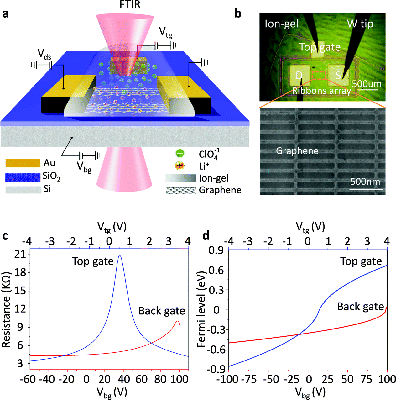 | ||
| Fig. 1 (a) Schematic of the experiment for measuring the extinction spectra of the ion-gel top-gated graphene nanoribbon array by FTIR microscopy. Highly doped Si and SiO2 were used as the back gate and dielectric in the same device for comparison. (b) Top: Optical micrograph of a fabricated device coated with the ion-gel film (green waves). Bottom: Scanning electron microscopy (SEM) image of a graphene nanoribbon array with a ribbon width of ∼65 nm and a gap-to-ribbon ratio of 1:1. (c) Representative transfer characteristics of the device controlled by the top gate voltage Vtg (blue curve) and the back gate voltage Vbg (red curve), respectively. (d) The dependence of the graphene Fermi levels on Vtg and Vbg, respectively. | ||
Using an ion-gel top gate can shift the Fermi level of graphene in a wide range with small gate voltages because of the high capacitance of the ion-gel. This high capacitance results from the nanometer thick (1–5 nm) Debye layer formed at the ion-gel/graphene interface.35–38 As illustrated in Fig. 1a, with a positive gate bias, negative ions (ClO4−) in the ion-gel move toward and accumulate near the top-gate electrode while the positive ions (Li+) accumulate on the surface of the graphene channel. The accumulated Li+ ions create a positive electric field, which draws electrons into the graphene channel. When a negative voltage is applied, holes are injected into graphene. Thus, by using the ion-gel top gate, we were able to obtain highly doped graphene nanoribbons with actively tunable carrier densities via small gate voltages. In addition, the applied gate voltages should be limited in the range from −5 to 5 V in order to prevent unwanted chemical reactions.39
The plasmonic properties of graphene at different Fermi levels EF were characterized by using Fourier transform infrared microscopy (FTIR). First, the extinction spectra (T(CNP)) of the graphene nanoribbon array at the charge neutral point (CNP) (i.e. EF = 0) were detected. Then we changed EF of the graphene nanoribbon array, and measured its extinction spectra T(EF). The electromagnetic response of the graphene plasmon at EF was obtained from the extinction spectrum T, where T = 1 − T(EF)/T(CNP). Since the background IR extinction was all cancelled out, the peaks in the as-obtained extinction spectrum resulted from the plasmon resonances which were strongly dependent on the electronic properties of the graphene.
Electrical characteristics
Gate voltage-dependent resistance properties of the graphene devices were detected by applying a top gate and a back gate, respectively, as shown in Fig. 1c. The CNP appears at 98 V by sweeping the back-gate voltage from −100 to 100 V (blue carve) while it appears at 0.53 V in the transfer characteristics of the same graphene sample with an ion-gel top-gate (red carve). The device was found to be a typical ambipolar FET as manifested by the ‘V’ shape of the resistance dependence on the gate voltage. The graphene at zero gate voltage was found to be highly p-type doped. This can be attributed to the absorption of impurities (e.g. water molecules)40 and the effect of surface dangling bonds of the SiO2 substrate.41,42 In addition, the maximum resistivity was found to increase after the ion-gel was spin coated. This phenomenon likely originated from the additional impurities introduced into the graphene by the ion-gel.35From the determined transfer characteristics, and the capacitance and thickness of the dielectric, we calculated the carrier concentration and EF of the graphene using a standard parallel plate capacitor model (see details below). For the SiO2 thin film, using a relative dielectric constant of 3.9 and a thickness of 300 nm, the capacitance was calculated as 0.0121 μF cm−2.15 The capacitance of the ion-gel dielectric was calculated as 2.42 μF cm−2 from a relationship that the shift in the back-gate voltage at CNP (Vbg, CNP) is linearly dependent on the change of the applied top-gate voltage (Vtg) and 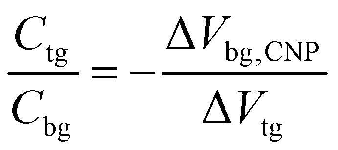 (see Fig. S3 in the ESI†). Based on the value of capacitance, the dielectric constant of the ion-gel can be calculated by using the conventional capacitance equation,
 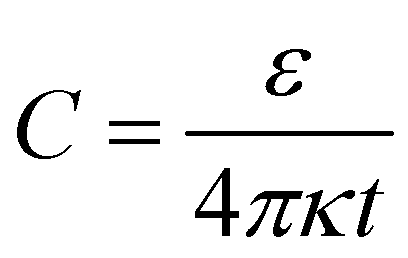 , where k is the static dielectric constant and t is the thickness of the Debye layer. Assuming a Debye length of 2 nm,30 we obtained the dielectric constant as 5.5 for the ion-gel composed of LiClO4 and PEO, which is consistent with previous reported values of PEO (∼5).43
For both the top-gated and back-gated graphene FET, the dependence of the carrier density on the gate voltage satisfies the equation:26,27,35
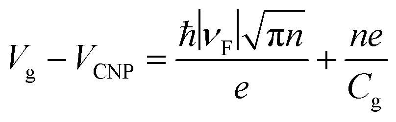
 , we obtained the relation between EF and the gate voltages (see the ESI†). As shown in Fig. 1d, EF is plotted as a function of both the ion-gel top-gate voltage (Vtg) and the SiO2 back-gate voltage (Vbg). When the Vtg is tuned from −4 to 4 V, the values of EF shifts from about −0.94 to 0.81 eV. This shift in EF is much larger than the change made by the back gate, which is about −0.5 to 0.05 eV with Vbg shifted from −100 to 100 V.
Plasmon resonance frequencies characteristics
The plasmonic properties of the as-prepared low voltage-controlled and broadly tunable mid-infrared graphene devices were experimentally characterized for performance. Because the electrical tunability of graphene is symmetric with respect to the CNP, we focused on the hole-doping regime for simplicity. Fig. 2a shows the extinction spectra of the graphene nanoribbon array at different EF controlled by the ion-gel top gate. The extinction spectra of the same graphene nanoribbon array at different EF controlled by the SiO2 back gate are used for comparison (Fig. 2b). In both the top-gated and back-gated strategies, there are two distinct resonance peaks in the extinction spectra, as indicated by diamonds and spheres in Fig. 2a and b. These peaks are ascribed to the coupling of graphene plasmons to two surface optical (SO) phonons of SiO2 at 806 cm−1 (ωsp1) and 1168 cm−1 (ωsp2), respectively.45,46 In order to better compare the electrical tunability of graphene plasmons controlled by the ion-gel and SiO2, we used narrow graphene ribbons (∼65 nm) to reduce this obvious plasmon–phonon coupling by shifting the pristine plasmon resonance frequency of graphene to energies much higher than ωsp2. In most of these extinction spectra (except for the conditions at low Fermi levels), the first resonance peaks (diamonds) are phonon-like polaritons (PP) and the second ones (spheres) are graphene plasmon-like polaritons (GP), which are the main peaks in the extinction spectra.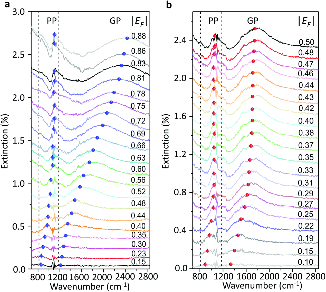 | ||
| Fig. 2 (a) Extinction spectra (T = 1 − T(EF)/T(CNP)) of the graphene nanoribbon array at various values of EF controlled by the ion-gel top gate. (b) Extinction spectra of the same device at various EF values controlled by the back gate. These spectra were characterized before the ion-gel film was coated on the device. The absorption peaks of CO2 (ranging from 2244 to 2395 cm−1) in ambient air were replaced by straight lines. | ||
The resonance frequency ωpl for pristine graphene plasmons is determined by EF and the wave vector q via the equation  ,7,19,47 where q = π/W. When q is fixed, the corresponding value of ωpl scales as EF1/2. For the plasmon–phonon coupling system, when EF of graphene increases, both the PP and the GP peaks gain intensity and shift to higher frequencies, as shown in Fig. 2. The plasmon resonance frequencies of the graphene device controlled by the ion-gel top gate are lower than those of the same device at the same EF controlled by the SiO2 back gate (see ESI Fig. S4†). This is due to the different effective dielectric environments of graphene for these two cases as the environment determines the plasmon resonance frequencies via ω ∝ ε−1/2. For the SiO2 back gate system (air/graphene/SiO2), the average dielectric environment
  , while for the ion-gel top gate system (ion-gel/graphene/SiO2),
  .
.
We used a generalized random phase approximation (RPA) theory to calculate the relationship between EF and the graphene plasmon resonance frequency under the conditions of plasmon–phonon coupling.45,48–50 Calculations were performed according to Yang et al.33Fig. 3a shows the calculated results for a graphene nanoribbon with 65 nm ribbon width at varying EF as controlled by both the ion-gel dielectric top gate (blue lines) and the SiO2 back gate (red lines) alongside the experimental data (diamonds and spheres) extracted from the extinction spectra of Fig. 2a and b. The two-dimensional pseudo-colour background was calculated from the loss function of the graphene plasmons controlled with the ion-gel dielectric top gate. The simulation results are in excellent agreement with our experimental results. The used Fröhlich-like coupling strength between plasmons and two SO phonons of SiO2 are presented in Fig. S5† (for the ion-gel top gate and for the SiO2 back gate). A small deviation between experimental and theoretical values mainly originates from the effect of the phonon–photon coupling of the SiO2 substrate and the calculation error of the ion-gel dielectric constant.
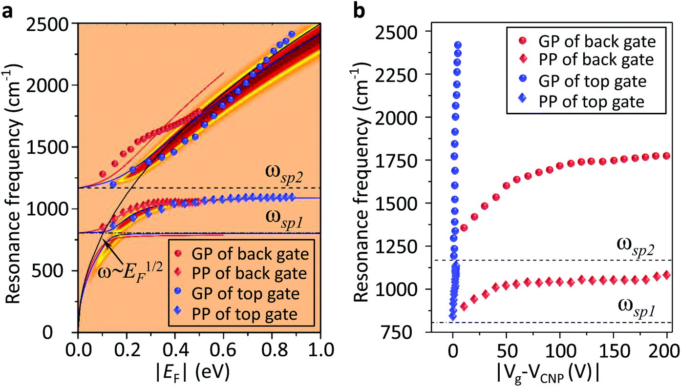 | ||
| Fig. 3 (a) The calculated resonance frequencies of PP and GP peaks as a function of EF controlled by the top gate (blue curves) and the back gate (red curves), respectively. The two-dimensional pseudo-colour background is calculated from the loss function of graphene plasmons controlled by the ion-gel top gate. The experimental data of PP (diamonds) and GP (spheres) peaks extracted from Fig. 2a and b are also plotted. (b) The dependence of the resonance frequencies of PP and GP peaks on the voltage of Vtg and Vbg shifted from the corresponding CNP, respectively. Two SO phonons of SiO2 are indicated by dashed lines. | ||
The plasmon resonance frequencies were plotted as a function of gate voltage shifted from CNP for both the SiO2 back gate (red) and ion-gel top gate (blue), respectively (Fig. 3b). The GP peak dramatically shifts from 1184 to 2455 cm−1 (Δω = 1271 cm−1) and the PP peak shifts from 842 to 1119 cm−1 (Δω = 277 cm−1) by adjusting Vtg to shift 4 V from CNP. In contrast, the GP peak shifts from 1374 to 1753 cm−1 (Δω = 379 cm−1) and the PP peak shifts from 906 to 1065 cm−1 (Δω = 159 cm−1) when Vbg shifts 200 V from CNP. The obtained shift of the GP peak by the ion-gel top gate is nearly 3.5 times as much as the value obtained by the SiO2 back gate while the applied voltage is just 1/50th of the latter.
Plasmon–phonon coupling between graphene and the ion-gel
Graphene plasmons in the mid-infrared spectral range can interact strongly with phonons of the surrounding dielectrics, such as the SO phonons of SiO2 and the optical phonons of h-BN.33,51 These strong plasmon–phonon couplings impede the electrostatic tunability of graphene plasmons significantly, especially at around the phonon energies. Thus, to explore how the ion-gel phonons affect graphene plasmons is of great importance. As shown in Fig. 4a, the molecular vibration modes of the ion-gel can also interact with the graphene plasmon mode. However, the resulting shape is completely different from the case when SiO2 phonons couple with graphene plasmons. The SiO2 phonons split the plasmon resonance peak into well separated multi-peaks (the PP peaks and the GP peaks), while ion-gels only introduce several shallow dips appearing in the extinction spectra (Fig. 4a). The most obvious dips at 844, 1118, 1280 and 2885 cm−1 are accompanied by other dips at 946, 974, 1061, 1154, 1233, 1344, 1363, 1469, and 1610 cm−1. These dips correspond to the respective IR group vibrations of PEO based on a comparison with the IR absorption peaks of the ion-gel thin film. In order to exhibit these plasmon–phonon coupling signals more clearly, zoom-in spectra of Fig. 4a in the range from 1000 to 1500 cm−1 (between the two dashed lines) are shown in Fig. 4b. The strong C–O–C stretching mode at ∼1118 cm−1 of PEO molecules couples with graphene plasmons and slightly splits the PP peak.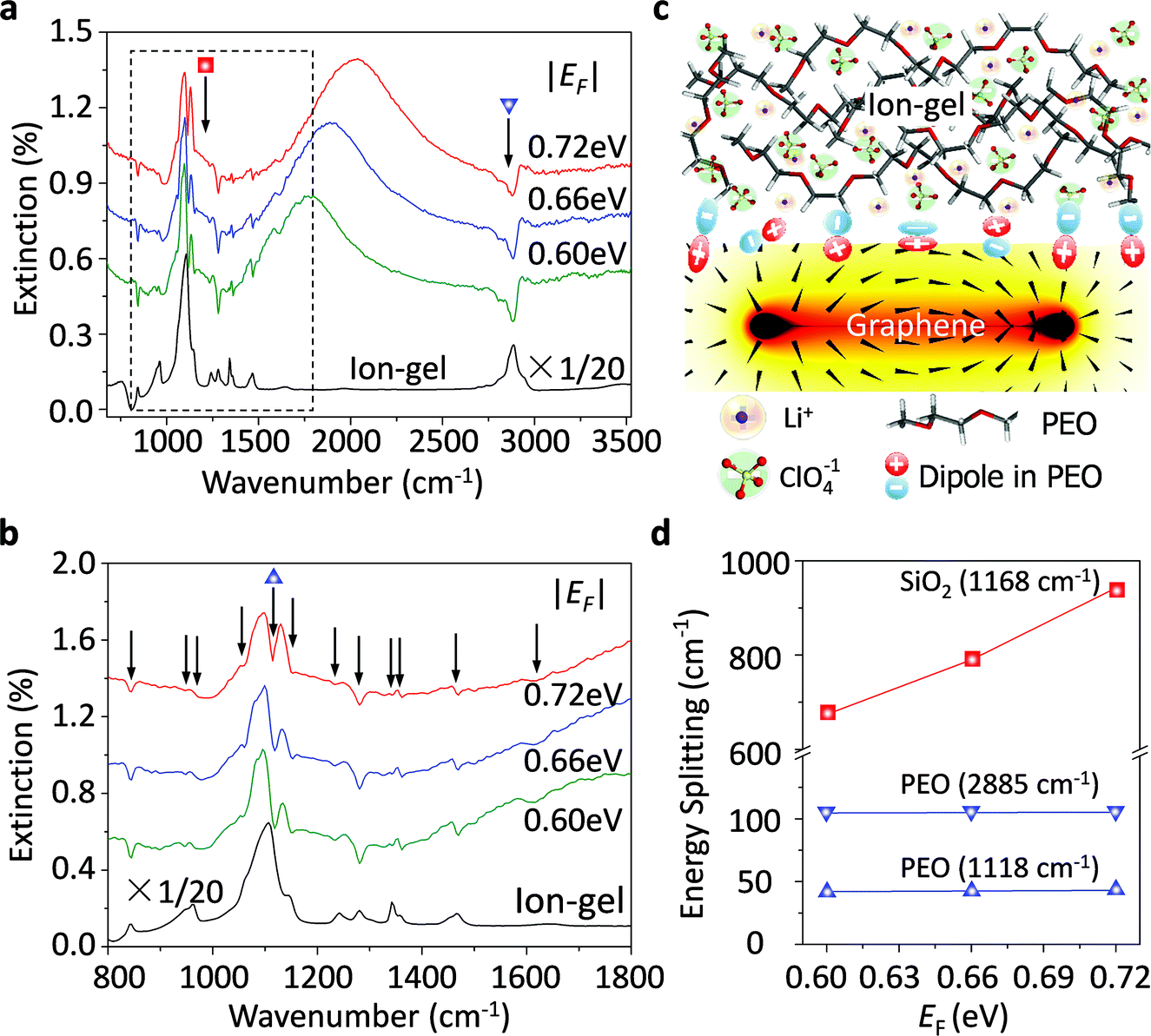 | ||
| Fig. 4 (a) Three selected extinction spectra of the graphene nanoribbon array at different EF controlled by an ion-gel top gate with an enlarged view. The infrared extinction spectrum of the ion-gel film is shown for comparison. The arrow under a red square indicates the SO phonons of SiO2 at 1168 cm−1. The arrow under the blue triangle indicates the molecular resonance of PEO at 2885 cm−1. (b) The zoom-in spectra of (a) illustrating the coupling between graphene plasmons and the dipole moments of C–O–C stretching vibration of PEO molecules. The arrows indicate the IR active molecular resonances of PEO. (c) Schematic of the coupling mechanism of graphene plasmons and PEO optical phonons. (d) Dependence of energy splitting induced by plasmon–phonon coupling on Fermi levels. For the graphene/PEO case, the deepest dips at 1118 (blue triangles, up) and 2885 cm−1 (blue triangles, down) are selected as instances. | ||
When the plasmon mode interacts with a phonon mode, the coupling of external light to the phonon mode (i.e. phonon absorption) can be significantly enhanced due to the plasmon excitation via the near field enhancement.13 The induced phonon resonances form polariton waves with an opposite phase with respect to the plasmon polaritons (Fig. 4c). These two waves with the same wavelength and opposite phase cause coherent destructive interference between them, which results in dips in the plasmon resonance extinction peaks. According to the interference theory of waves, the shape of the dips is mainly determined by the intensity of the induced phonon polariton waves, which determined the coupling strengths. For the plasmon–phonon polaritons, the coupling strength is proportional to the energy splitting of the dip.52Fig. 4d presents the dependence of the energy splitting on the Fermi levels for both graphene/PEO and graphene/SiO2 systems. For both cases, the coupling strength increases coinciding with the shift of the Fermi level, that is the increasing electromagnetic field strength of graphene plasmons. For the graphene/PEO system, the coupling strength is much less than that of graphene/SiO2. The latter enters a strong coupling regime as the splitting energies are much larger than the sum of the linewidths of graphene plasmons and SiO2 phonons. The former is a weak coupling system as the splitting energy is much less than the sum of the linewidths of graphene plasmons and the phonon resonance. This is because the densities of phonon modes in the ion-gel are much smaller than those in the SiO2 films due to a disordered arrangement of long PEO molecular chains (Fig. 4c), which is consistent with the coupling between plasmons and other molecular vibrations.53 Thus, compared with conventional oxide dielectric materials, an ion-gel dielectric has very limited perturbation on the properties of graphene plasmons.
Plasmon lifetime characteristics
The influence of the ion-gel dielectric on plasmon lifetimes, which is closely related to the plasmonic performance, was also studied. The plasmon lifetime T can be obtained via T = 2ħ/Γ for the far field extinction spectra,33,54 where Γ is the linewidth of the resonance peaks extracted by using Fano curve fitting (see the ESI and Fig. S6a†). We compared the graphene plasmon lifetimes of the graphene/SiO2 device before and after spin coating with the ion-gel top gate by plotting the lifetimes of the GP mode as a function of resonance frequencies (Fig. S6b†). In both the systems, the lifetimes dramatically decreased as the resonance frequencies increased. The lifetimes increased slightly at the same resonance frequency after adding the ion-gel film. This is because the ion-gel coating introduces additional scattering (such as charged impurities) to the graphene plasmons. The condition is very similar to that of free standing graphene transferred onto supporting substrates, whose carrier mobility decreases dramatically due to the introduced phonon scattering and charged impurity scattering. However, the mobility of graphene is less reduced by ion gels due to its weak phonon scattering.Conclusions
In conclusion, we achieved a low voltage-controlled and broadly tunable graphene plasmonic device with a top gate prepared by a simple and convenient method of using a spin-coated ion-gel thin film as a dielectric. The ion-gel top gate can shift the plasmon resonance frequency to 1271 cm−1 which is nearly 3.5 times the value obtained by a SiO2 back gate (379 cm−1) while applying 1/50th of the voltage shifted from the CNP (e.g. 4 V compared to the 200 V required for a SiO2 back gate). In addition, unlike the graphene plasmon resonance peaks being split by the SO phonons of SiO2 and the optical phonons of h-BN, the coupling between a graphene plasmon and phonons of PEO is much weaker and has very limited effects on the plasmonic properties. On the whole, the ion-gel is an excellent dielectric for broadly tunable graphene plasmon devices.Experimental section
The device consists of a graphene sheet prepared by chemical vapor deposition (CVD) on copper foil which was transferred onto a SiO2 (300 nm)/Si substrate. The sample was identified to be a monolayer by using a micro-Raman microscope (Horiba JobinYvon, LabRAM HR800) before processing. The nanoribbon arrays were patterned using electron-beam lithography on graphene which was then etched away using oxygen plasma. The graphene nanoribbons were characterized by atomic force microscopy (s-SNOM, Neaspec) using tapping mode and SEM (Hitachi, S-4800). The source, drain and top gate electrodes of the device were made by e-beam lithography, followed by e-beam evaporation of 100 nm of gold and subsequent lift-off in acetone. The ion-gel dielectric material was achieved by dissolving polyethylene oxide (PEO) and LiClO4 in methanol with a mass ratio of 1:0.12:40, as reported in previous work.27,35 The compounded ion-liquid is then spun onto a graphene transistor at 5000 RPM, followed by baking at 60 °C to remove any residual methanol. The electrical transport properties were characterized with a semiconductor parameter analyzer (Agilent, 4294A). Vtg was applied by inserting a wolframium electrode within the polymer layer. The measurement set-up for the device consisted of an infrared microscope coupled to a Fourier-transform infrared spectrometer (ThermoFisher, Nicolet iN10), used in conjunction with a power source (Keithley 2612B). All the measurements were performed at room temperature and under an ambient atmosphere. The finite element method was used to simulate the plasmonic responses of the devices.
Acknowledgements
This work was supported by the National Basic Research Program of China (Grant No. 2015CB932400), the National Natural Science Foundation of China (Grant No. 51372045, and No. 11174252) and the Bureau of International Cooperation, Chinese Academy of Sciences (121D11KYSB20130013).Notes and references
- Q. Bao and K. P. Loh, ACS Nano, 2012, 6, 3677 CrossRef CAS PubMed.
- T. Stauber, J. Phys. Condens. Matter, 2014, 26, 123201 CrossRef PubMed.
- F. MinovKoppensich, D. Chang, S. Thongrattanasiri and F. García de Abajo, Opt. Photonics News, 2011, 22, 36 CrossRef.
- T. Low and P. Avouris, ACS Nano, 2014, 8, 1086 CrossRef CAS PubMed.
- X. Luo, T. Qiu, W. Lu and Z. Ni, Mater. Sci. Eng., R, 2013, 74, 351 CrossRef.
- M. Jablan, M. Soljacic and H. Buljan, Proc. IEEE, 2013, 101, 1689 CrossRef CAS.
- A. Grigorenko, M. Polini and K. Novoselov, Nat. Photonics, 2012, 6, 749 CrossRef CAS.
- F. J. Garcia de Abajo, ACS Photonics., 2014, 1, 135 CrossRef CAS.
- F. Bonaccorso, Z. Sun, T. Hasan and A. Ferrari, Nat. Photonics, 2010, 4, 611 CrossRef CAS.
- B. Sensale-Rodriguez, R. Yan, M. M. Kelly, T. Fang, K. Tahy, W. S. Hwang, D. Jena, L. Liu and H. G. Xing, NatCommun., 2012, 3, 780 Search PubMed.
- S. Badhwar, R. Puddy, P. R. Kidambi, J. Sibik, A. Brewer, J. R. Freeman, H. E. Beere, S. Hofmann, J. A. Zeitler and D. Ritchie, IEEE Photonics J., 2012, 4, 1776 CrossRef.
- L. Ju, B. Geng, J. Horng, C. Girit, M. Martin, Z. Hao, H. A. Bechtel, X. Liang, A. Zettl, Y. R. Shen and F. Wang, Nat. Nanotechnol., 2011, 6, 630 CrossRef CAS PubMed.
- H. Yan, X. Li, B. Chandra, G. Tulevski, Y. Wu, M. Freitag, W. Zhu, P. Avouris and F. Xia, Nat. Nanotechnol., 2012, 7, 330 CrossRef CAS PubMed.
- L. Vicarelli, M. Vitiello, D. Coquillat, A. Lombardo, A. Ferrari, W. Knap, M. Polini, V. Pellegrini and A. Tredicucci, Nat. Mater., 2012, 11, 865 CrossRef CAS PubMed.
- H. Xu, Z. Zhang, H. Xu, Z. Wang, S. Wang and L.-M. Peng, ACS Nano, 2011, 5, 5031 CrossRef CAS PubMed.
- K. S. Novoselov, A. K. Geim, S. Morozov, D. Jiang, Y. Zhang, S. a. Dubonos, I. Grigorieva and A. Firsov, Science, 2004, 306, 666 CrossRef CAS PubMed.
- A. K. Geim and K. S. Novoselov, Nat. Mater., 2007, 6, 183 CrossRef CAS PubMed.
- J. Liu, Q. Qian, Y. Zou, G. Li, Y. Jin, K. Jiang, S. Fan and Q. Li, Carbon, 2014, 68, 480 CrossRef CAS.
- S. Badhwar, J. Sibik, P. R. Kidambi, H. E. Beere, J. A. Zeitler, S. Hofmann and D. A. Ritchie, Appl. Phys. Lett., 2013, 103, 121110 CrossRef.
- Y. Zhang, T.-T. Tang, C. Girit, Z. Hao, M. C. Martin, A. Zettl, M. F. Crommie, Y. R. Shen and F. Wang, Nature, 2009, 459, 820 CrossRef CAS PubMed.
- K. Zou, X. Hong, D. Keefer and J. Zhu, Phys. Rev. Lett., 2010, 105, 126601 CrossRef CAS PubMed.
- A. Konar, T. Fang and D. Jena, Phys. Rev. B: Condens. Matter, 2010, 82, 115452 CrossRef.
- L. Liao, J. Bai, Y. C. Lin, Y. Qu, Y. Huang and X. Duan, Adv. Mater., 2010, 22, 1941 CrossRef CAS PubMed.
- S. Kim, J. Nah, I. Jo, D. Shahrjerdi, L. Colombo, Z. Yao, E. Tutuc and S. K. Banerjee, Appl. Phys. Lett., 2009, 94, 062107 CrossRef.
- J. Bai, L. Liao, H. Zhou, R. Cheng, L. Liu, Y. Huang and X. Duan, Nano Lett., 2011, 11, 2555 CrossRef CAS PubMed.
- B. Chakraborty, A. Das and A. Sood, Nanotechnology, 2009, 20, 365203 CrossRef PubMed.
- J. Liu, Q. Li, Y. Zou, Q. Qian, Y. Jin, G. Li, K. Jiang and S. Fan, Nano Lett., 2013, 13, 6170 CrossRef CAS PubMed.
- M. A. B. H. Susan, T. Kaneko, A. Noda and M. Watanabe, J. Am. Chem. Soc., 2005, 127, 4976 CrossRef CAS PubMed.
- S.-K. Lee, S. H. Kabir, B. K. Sharma, B. J. Kim, J. H. Cho and J.-H. Ahn, Nanotechnology, 2014, 25, 014002 CrossRef PubMed.
- J. H. Cho, J. Lee, Y. Xia, B. Kim, Y. He, M. J. Renn, T. P. Lodge and C. D. Frisbie, Nat. Mater., 2008, 7, 900 CrossRef CAS PubMed.
- N. K. Emani, T.-F. Chung, A. V. Kildishev, V. M. Shalaev, Y. P. Chen and A. Boltasseva, Nano Lett., 2013, 14, 78 CrossRef PubMed.
- Z. Fang, S. Thongrattanasiri, A. Schlather, Z. Liu, L. Ma, Y. Wang, P. M. Ajayan, P. Nordlander, N. J. Halas and F. J. García de Abajo, ACS Nano, 2013, 7, 2388 CrossRef CAS PubMed.
- X. Yang, F. Zhai, B. Bai, H. Hu, J. Chen and Q. Dai, arXiv preprint arXiv:1504.00195, 2015.
- A. Pachoud, M. Jaiswal, P. K. Ang, K. P. Loh and B. Oezyilmaz, EPL-Europhys. Lett., 2010, 92, 27001 CrossRef.
- A. Das, S. Pisana, B. Chakraborty, S. Piscanec, S. Saha, U. Waghmare, K. Novoselov, H. Krishnamurthy, A. Geim and A. Ferrari, Nat. Nanotechnol., 2008, 3, 210 CrossRef CAS PubMed.
- B. J. Kim, H. Jang, S.-K. Lee, B. H. Hong, J.-H. Ahn and J. H. Cho, Nano Lett., 2010, 10, 3464 CrossRef CAS PubMed.
- J. Ye, M. F. Craciun, M. Koshino, S. Russo, S. Inoue, H. Yuan, H. Shimotani, A. F. Morpurgo and Y. Iwasa, Proc. Natl. Acad. Sci. U. S. A., 2011, 108, 13002 CrossRef CAS PubMed.
- X. He, N. Tang, L. Gao, J. Duan, Y. Zhang, F. Lu, F. Xu, X. Wang, X. Yang and W. Ge, Appl. Phys. Lett., 2014, 104, 143102 CrossRef.
- J. Lee, M. J. Panzer, Y. He, T. P. Lodge and C. D. Frisbie, J. Am. Chem. Soc., 2007, 129, 4532 CrossRef CAS PubMed.
- J. Kong, N. R. Franklin, C. Zhou, M. G. Chapline, S. Peng, K. Cho and H. Dai, Science, 2000, 287, 622 CrossRef CAS PubMed.
- Y. Shi, X. Dong, P. Chen, J. Wang and L.-J. Li, Phys. Rev. B: Condens. Matter, 2009, 79, 115402 CrossRef.
- T. O. Wehling, M. I. Katsnelson and A. I. Lichtenstein, Appl. Phys. Lett., 2008, 93, 202110 CrossRef.
- R. H. Boyd, J. Polym. Sci., Polym. Phys. Ed., 1983, 21, 505 CrossRef CAS.
- C. Hwang, D. A. Siegel, S.-K. Mo, W. Regan, A. Ismach, Y. Zhang, A. Zettl and A. Lanzara, Sci. Rep., 2012, 2, 590 Search PubMed.
- H. Yan, T. Low, W. Zhu, Y. Wu, M. Freitag, X. Li, F. Guinea, P. Avouris and F. Xia, Nat. Photonics., 2013, 7, 394 CrossRef CAS.
- X. Yang, X. T. Kong, B. Bai, Z. Li, H. Hu, X. Qiu and Q. Dai, Small, 2015, 11, 591 CrossRef CAS PubMed.
- S. H. Abedinpour, G. Vignale, A. Principi, M. Polini, W.-K. Tse and A. MacDonald, Phys. Rev. B: Condens. Matter, 2011, 84, 045429 CrossRef.
- E. Hwang, R. Sensarma and S. D. Sarma, Phys. Rev. B: Condens. Matter, 2010, 82, 195406 CrossRef.
- M. Jablan, M. Soljačić and H. Buljan, Phys. Rev. B: Condens. Matter, 2011, 83, 161409 CrossRef.
- E. Hwang and S. D. Sarma, Phys. Rev. B: Condens. Matter, 2007, 75, 205418 CrossRef.
- V. W. Brar, M. S. Jang, M. Sherrott, S. Kim, J. J. Lopez, L. B. Kim, M. Choi and H. Atwater, Nano Lett., 2014, 14, 3876 CrossRef CAS PubMed.
- Y. Jia, H. Zhao, Q. Guo, X. Wang, H. Wang and F. Xia, ACS Photonics, 2015, 2, 907 CrossRef CAS.
- F. Neubrech, A. Pucci, T. W. Cornelius, S. Karim, A. García-Etxarri and J. Aizpurua, Phys. Rev. Lett., 2008, 101, 157403 CrossRef PubMed.
- C. Sonnichsen, T. Franzl, T. Wilk, G. von Plessen, J. Feldmann, O. Wilson and P. Mulvaney, Phys. Rev. Lett., 2002, 88, 077402 CrossRef CAS PubMed.
Footnote |
| † Electronic supplementary information (ESI) available. See DOI: 10.1039/c5nr05175d |
| This journal is © The Royal Society of Chemistry 2015 |