Visible light driven type II heterostructures and their enhanced photocatalysis properties: a review
Yajun
Wang
,
Qisheng
Wang
,
Xueying
Zhan
,
Fengmei
Wang
,
Muhammad
Safdar
and
Jun
He
*
National Center for Nanoscience and Technology, Beijing 100190, P. R. China. E-mail: hej@nanoctr.cn
First published on 21st May 2013
Abstract
Considerable efforts have been devoted to enhancing the photocatalytic activity and solar energy utilization of photocatalysts. The fabrication of type II heterostructures plays an important role in photocatalysts modification and has been extensively studied. In this review, we briefly trace the application of type II heterostructured semiconductors in the area of environmental remediation and water splitting, summarize major fabrication methods, describe some of the progress and resulting achievements, and discuss the future prospects. The scope of this review covers a variety of type II heterostructures, focusing particularly on TiO2 and ZnO based visible light driven type II 0D and 1D heterostructured photocatalysts. Some other low dimensional nanomaterials which have shown high-performance photocatalysis are also presented. We expect this review to provide a guideline for readers to gain a clear picture of fabrication and application of type II heterostructures.
 Yajun Wang | Yajun Wang received her BS degree in Environmental Engineering from Tsinghua University in 2006. She received her PhD degree in Chemistry from Tsinghua University in 2011. Currently, she is an assistant professor in National Center of Nanoscience and Technology (NCNST), China. Her research interests include development and modification of photocatalysts for environmental purification and water splitting. |
 Jun He | Jun He received his PhD in physical chemistry from the Institute of Semiconductors, Chinese Academy of Sciences in 2003. Dr He is presently a Professor of physical chemistry of materials in the National Center for Nanoscience and Technology, China, with research interests in low dimensional semiconductor materials synthesis, characterization, and devices. |
1 Introduction
Environmental and energy issues are among the biggest challenges in the new century. With the growth of worldwide industry, severe environmental contaminations have become a major concern of our society. The development of high efficiency, green energy sources and eco-friendly methods for environmental remediation has become an imperative task. Moreover, energy shortages and surging green-house gas (GHG) emissions have been two of the major challenges the world is facing today. For example, in China over 70% of domestic energy originates from coal. As a result, China suffers from a series of environmental problems and public health crises due to the burning of fossil fuel. In order to solve these severe problems, China has set goals to mitigate its CO2 emission per unit of Gross Domestic Production (GDP) by 40–45% by 2020, with an interim target in the 12th 5-Year Plan of 17% by 2015.1Among various strategies, finding renewable energy, instead of fossil fuel is the key measure. Hydrogen, as a clean and non-carbon energy source, is of great potential in solving the environmental crisis and energy shortage. As a result, photocatalysis, as one of the promising technologies in utilizing solar energy to solve environmental and energy issues, has attracted considerable attention.
Fujishima and Honda first reported the UV light induced photo-assisted decomposition of water into hydrogen and oxygen using a titanium dioxide photoanode in electrochemical cell in 1972.2 Since then, semiconductor photocatalysis has attracted widespread attention in scientific community due to its potential application in environmental remediation and hydrogen production. The basic mechanisms of photocatalysis have been established and reported in many literature accounts.3,4 Taking TiO2 as an example, the mechanism of the photocatalytic process is shown in Fig. 1.
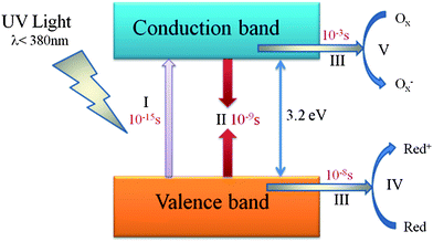 | ||
| Fig. 1 Primary steps in the photocatalytic mechanism (TiO2): (I) formation of electron (e−)–hole (h+) pairs by photoexcitation; (II) photoinduced charge recombination; (III) photoinduced charge transportation; (IV) oxidation caused by a valence band hole; (V) reduction caused by a conduction band electron (adapted with permission from ref. 3, copyright 1995 American Chemical Society). | ||
When the absorbed photon has an energy equaling or exceeding the band gap energy (Eg) of TiO2, an electron in the filled valence band (VB) is excited into the empty conduction band (CB), leaving behind a hole in VB (stage I). Stage II and stage III occur in parallel, but the recombination process (stage II) is much faster than the transportation process (stage III) as shown in Fig. 1. After the electrons and holes transfer to the active sites of the surface of TiO2, they will act as reducing/oxidizing agents to drive reduction/oxidation on the surface (stage VI and V). In detail, at stage VI and V, for photocatalytic degradation of pollutants, holes of VB can react with surface adsorbed H2O to produce hydroxyl radicals. The hydroxyl radicals are strong oxidizing agents, which can oxidize almost all organic pollutants with no selectivity. Moreover, the holes can also directly oxidize the organic pollutants to form R+.3,5 For water splitting, water molecules are reduced by the photoinduced electrons to form H2 and are oxidized by the photoinduced holes to form O2. For effective water splitting, the bottom level of the CB of the semiconductor has to be more negative than the redox potential of H+/H2 (0 V vs. NHE), while the top level of the VB of the semiconductor should be more positive than the redox potential of O2/H2O (1.23 V vs. NHE). The minimum band gap for water splitting is 1.23 eV; theoretically, all types of semiconductors that satisfy the above requirements could be used as photocatalysts for water splitting. Particularly, in a photoelectrochemical (PEC) cell, carriers in the semiconductor should travel to an electrode/liquid junction to drive the hydrogen/oxygen evolution reaction. In electron-transfer processes at semiconductor/liquid junctions, unavoidable losses are caused by concentration and kinetic overpotentials. Therefore, accounting for the losses, the energy required for PEC water splitting at a semiconductor photoelectrode is calculated as 1.6–2.4 eV per electron–hole pair generated.6
Although semiconductor photocatalysis has made great progress during the past three decades, there are still some unsolved problems. Again, taking TiO2 as an example, TiO2 is known as the most widely investigated photocatalyst due to its high oxidative efficiency, high chemical stability, nontoxicity and low-cost.7–9 Presently, the photocatalytic degradation activity and water splitting efficiency of TiO2 is still low, mainly due to the following two reasons: (1) slow reaction rate: the photocatalytic reactions only occur when the photoinduced electrons and holes transfer to the surface active sites of the semiconductor. However, the recombination process is much faster than the transportation process, leading to low photocatalytic efficiency. (2) Poor solar energy utilization: TiO2 with a bandgap of 3.2 eV can be only excited by photons with light wavelengths shorter than about 400 nm in the UV wavelength range, which accounts for about 4% of the solar radiation energy.10,11 Therefore, a great deal of effort has been devoted to enhancing the efficiency of the photocatalytic process and extending the light adsorption range of TiO2, such as formation of semiconductor heterostructures,12,13 codeposition of noble metals,14,15 doping,16,17 surface hybridization18–20 and coupling with other technology.19,20 Among these approaches, formation of semiconductor heterostructures is an effective way to enhance the photoinduced charges separation efficiency and the photocatalytic performance, and has been extensively studied for the last decades. Depending on the bandgaps and the electronic affinity of semiconductors, semiconductor heterostructures can be divided into three different cases: type-I, type-II and type-III band alignment as shown in Fig. 2.
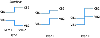 | ||
| Fig. 2 Schematic energy band diagram of three types of semiconductor heterojunctions. | ||
In a type-II band alignment, the position of valance and conduction bands of semiconductor 2 is higher than that of semiconductor 1, and the steps in the conduction and valance bands go in the same direction. Importantly, the difference of chemical potential between semiconductor 1 and 2 causes band bending at the interface of junction. The band bending induces a built-in field, which drives the photogenerated electrons and holes to move in opposite directions, leading to a spatial separation of the electrons and holes on different sides of heterojunction.21 Thus, the formation of type-II heterostructures is an effective approach to enhance charge separation efficiency for improved photocatalytic degradation activity and water splitting efficiency.
Moreover, a UV excited semiconductor (such as TiO2, ZnO, ZnWO4) coupled with a visible light excited semiconductor (a narrow bandgap semiconductor such as CdS, CdSe, CdSSe, C3N4) can effectively improve its solar energy utilization efficiency because the synergic absorption of two semiconductors with different band gaps extends the light response range to the whole solar spectrum. There are two prerequisite conditions to prepare a visible light driven type II heterostructure: (1) the outer shell material should have a strong visible light absorption (photo-sensitizer), and (2) the band alignment at the interface between the outer shell material and inner core should satisfy the conditions of type II heterostructures. In addition, the crystal structure in the junction area of the heterostructure is found to be important in enhancing the quantum efficiency of the photocatalyst. A difference in lattice spacing between two semiconductors is likely cause lattice mismatch. The lattice mismatch at the interface may cause defects, which trap the photogenerated carriers and thus prevent the diffusion of electrons and holes. However, interface strain arising from the lattice mismatch also alters the electronic structure. Indeed, lattice strain could induce an electric field, which further improves the separation efficiency of electrons and holes.22 Consequently, careful selection of materials should be taken before preparing visible light driven type II heterostructures. Fig. 3 shows the band edge position of several widely used semiconductors.23 The type-II heterostructure has attracted widespread attention in fabrication, study of its properties, and applications. Diverse type-II heterostructures have been explored, such as composite nanoparticles,24–29 quantum dots in nanowires,30–32core/shell nanowires,33–35etc. Compared with pure semiconductors, these type-II heterostructures, such as CdS/TiO2,36,37 CdS/ZnO,38,39 ZnSe/ZnO,40 ZnS/ZnO,41 ZnO/TiO2/CuO,42 and SnO2/CdS43 have achieved higher photocatalytic efficiency and solar energy utilization. In this review, we briefly trace the application of type II heterostructured semiconductors in the area of environmental remediation and water splitting, summarize major fabrication methods, describe some of the progress and resulting achievements, and discuss the future prospects.
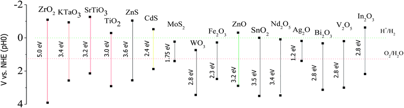 | ||
| Fig. 3 Band edge position of several semiconductors, using the normal hydrogen electrode (NHE) as a reference (adapted with permission from ref. 23, copyright 2009 Royal Society of Chemistry). | ||
2 Synthesis of type II heterostructures
Due to their wide application in the degradation of pollutants, energy conversion and water splitting, controllable synthesis of visible-light driven type II heterostructured photocatalysts have attracted tremendous attention. Over the past decades, various synthesis techniques, such as chemical vapor deposition,44 chemical deposition,45–47 electrodeposition, etc.,48 have been well developed and successfully used in preparing high-quality type II core/shell heterostructures.Compared with the synthesis of the core material, the growth of outer shell material (sensitizer) is more complicated. For example, different thicknesses of sensitizer may result in different photocatalytic properties.49 Therefore, in this section, we will focus our attention on methods for the synthesis of the sensitizer. Considering the wide application of ZnO and TiO2 as the photocatalysts, here we will mainly discuss the preparation of sensitizers based on ZnO and TiO2 nanostructured material. Other type II heterostructured photocatalysts prepared by special synthetic methods are also presented.
2.1 Chemical vapor deposition
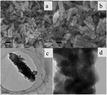
Vapor-phase synthesis is probably the most extensively explored approach in the field of nanofabrication. Chemical vapor deposition (CVD) or chemical vapor transport (CVT) is very commonly used for type II heterostructure synthesis. This method has the ability to control the sensitizer composition, thickness and stability by controlling several processing parameters such as temperature, pressure, carrier gas, substrate and evaporation time period. A number of type-II heterostructured sensitizers, for example, CdSe, CdSSe, ZnxCd1−xSe, ZnSxSe1−x, ZnSxSe1−x/ZnSe, ZnGa2O4 and ZnTe have been deposited on ZnO cores via the CVD method.44,50–54 In most cases, type II heterostructure can be obtained in two-step growth procedure. Firstly, the inner core semiconductor nanostructure is grown on a suitable substrate via CVD or another synthetic technique. In the second step, the substrate with pre-grown core nanostructure, is kept in a tube furnace to deposit the shell and under optimized conditions, controlled shell materials can be obtained. Myung and co-workers have reported 10 nm and 50 nm thick CdS shells on ZnO nanowires which were remarkably associated with time and temperature variation.50Our group has recently successfully synthesized a ZnSxSe1−x shell on a vertical ZnO nanowire array via the CVD method.44 Firstly, a single crystalline ZnO nanowire array was obtained on an Au deposited Si substrate using a two-zone furnace tube and mixed graphite and ZnO powder as sources. In the second step, a homogenous shell of ZnSxSe1−x was deposited on the exposed surface of ZnO by CVD. In detail, ZnS and ZnSe mixed in a 3![[thin space (1/6-em)]](https://www.rsc.org/images/entities/char_2009.gif) :7 mole ratio were used as the source in the center of a quartz tube keeping 8 cm of distance from the pre-grown ZnO nanowire substrate. The source was evaporated at 1100 °C and deposited on the ZnO nanowire array, and the shell thickness was carefully controlled by adhering to the optimum deposition time. The synthesized core/shell structure is presented in Fig. 4. Fig. 4a represents the ZnO nanowire before coating (inset of Fig. 4a) and after ZnSSe coating. X-ray EDS spectra demonstrate that the core and shell have an approximate 1:3 atomic ratio (Fig. 4b). Transmission electron microscopy (TEM) investigation confirms that the synthesized material was a typical core/shell structure and with a fine single crystalline structure as shown in Fig. 4c and d.
:7 mole ratio were used as the source in the center of a quartz tube keeping 8 cm of distance from the pre-grown ZnO nanowire substrate. The source was evaporated at 1100 °C and deposited on the ZnO nanowire array, and the shell thickness was carefully controlled by adhering to the optimum deposition time. The synthesized core/shell structure is presented in Fig. 4. Fig. 4a represents the ZnO nanowire before coating (inset of Fig. 4a) and after ZnSSe coating. X-ray EDS spectra demonstrate that the core and shell have an approximate 1:3 atomic ratio (Fig. 4b). Transmission electron microscopy (TEM) investigation confirms that the synthesized material was a typical core/shell structure and with a fine single crystalline structure as shown in Fig. 4c and d.
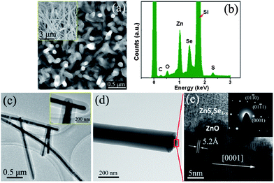 | ||
| Fig. 4 (a) SEM image of ZnSxSe1−x/ZnO core/shell nanowires, inset is a side-view SEM image of ZnO nanowires before coating, (b) an X-ray EDS of ZnSxSe1−x/ZnO core/shell nanowires. (c) and (d) TEM images of ZnSxSe1−x/ZnO core/shell nanowires along inset of enlarged head ends. (e) HRTEM images of a single ZnSxSe1−x/ZnO core/shell nanowire, inset SAED pattern of the core/shell nanowire (reprinted with permission from ref. 44, copyright 2012 American Institute of Physics). | ||
2.2 Chemical deposition
Chemical deposition is a simple and low cost method to fabricate type-II heterostructures. In this technique, the growth of thin films results from the bulk precipitation of the solution.55 Chalcogenide layers are usually prepared by this method. The temperature, pH, deposition time, and the concentration of the precursor play important roles in this method. Based on this method, some type II heterostructures can be easily obtained,56,57 such as CdS/TiO2,45 CdSe/CdS/ZnO,46 ZnxCd1−xS/ZnO,47 CdS/ZnS,58 g-C3N4/TiO2.59For example, TiO2/CdS heterostructure can be obtained by a chemical bath deposition method.45 Firstly, the TiO2 core was prepared by a hydrothermal method, and then further converted into an ITO substrate, which was vertically immersed in an aqueous bath containing 10 mL 0.02 M CdCl2·2.5H2O, 10 mL 0.2 M CH4N2S, 10 mL of 1.5 M NH4NO3and 10 mL 0.5 M KOH to deposit the CdS shell at 85 °C. Typical SEM and TEM images of the TiO2/CdS are shown in the Fig. 5. This facile method was also used in another example to fabricate heterostructured ZnxCd1−xS/ZnO.47 The morphologies of the ZnO/ZnxCd1−xS heterostructure could be controlled by altering the ratio of the ZnxCd1−xS precursors.
 | ||
| Fig. 5 SEM images of the as-prepared TiO2 nanorod film before (a) and after (b) coating with CdS nanoparticles at high magnification; TEM image of a single CdS/TiO2 core/shell nanorod (c) and high-resolution TEM image of a single CdS/TiO2 core/shell nanorod (d) (reprinted with permission from ref. 45, copyright 2007 Elsevier). | ||
2.3 Electrochemical deposition
Compared with the CVD method, electrochemical deposition allows large-scale nanostructure fabrication at low temperature. This conventional technique is most suitable for production of highly dense, uniform and ordered type-II heterostructured nanomaterials for large scale applications.60–64 The shell thickness of type-II heterostructures, which directly influences their performance, can be controlled by temperature, potential and time duration. For instance, Yao and co-workers reported that the thickness of CdS shell on ZnO nanorod can be controlled by this method via adjustment of deposition time.60 In addition, Wu and co-workers synthesized Co3O4 nanowires on Ni foil by a hydrothermal method and then used this material as the working electrode for electrodeposition of an NiO shell. Co3O4 nanowires can be covered by the NiO nanoflake shell when 0.25 mA cm−2 constant anodic current was applied for 1 h.64In the electrodeposition system, the pre-grown materials on indium-doped tin oxide (ITO), fluorine-doped tin oxide (FTO) or other relevant substrates is used as the working electrode. As a representative case, the large scale electrodeposition of a CdTe shell on a ZnO nanorod array was reported by Wang and co-workers.48 A thermally evaporated ZnO nanorod array on ITO was used as the working electrode, Pt foil as the counter electrode and saturated calomel electrode (SCE) as the reference electrode. Electrodeposition of the CdTe shell was completed by applying −1.0 V versus SCE in TeO32− and Cd2+ electrolyte solution with pH 8.3. The thickness of the CdTe shell was controlled by maintaining the total charge of the electrodeposition system. Fig. 6a and c display SEM images of the bare ZnO nanorod array. Fig. 6b and d show the SEM images of ZnO nanorods after CdTe electrodeposition. The TEM image in Fig. 6e reveals the smooth covering of the ZnO core with an 11 nm CdTe shell, and the HRTEM image in Fig. 6f depicts the crystalline structure of CdTe/ZnO nanocable. As demonstrated by these examples, electrochemical deposition is a suitable technique to fabricate controlled type-II heterostructures.
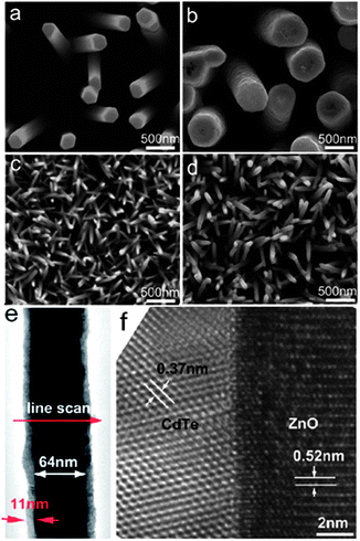 | ||
| Fig. 6 ZnO nanorod arrays (a) before and (b) after electrodeposition (160 nm thick shell) with total charge of 6.7 C; ZnO nanorod arrays (c) before and (d) after electrodeposition (11 nm thick shell) with total charge of 0.7 C. (e) Low-magnification TEM image showing the uniform morphology of a single CdTe/ZnO nanocable; (f) typical HRTEM image taken from the same CdTe/ZnO nanocable, showing the interface and crystalline structure of the nanocable (reprinted with permission from ref. 48, copyright 2010 American Chemical Society). | ||
2.4 Ion exchange
Ion exchange is a novel technique to prepare core/shell heterostructures by exchanging the ions at the interface of the heterostructure. In this method, the anion or cation is transferred into the nanostructure, then the shell is formed in gas or solution phase. In the process of cation exchange,65 external cations enter the parent crystal at the same time as the original cations diffuse out of the crystal. For example, Konenkamp and Dloczik have proved that the oxygen component of highly structured ZnO films can be replaced by S in the H2S phase and thus a ZnS shell with similar morphology to the initial ZnO was obtained.66 Meanwhile, through the exchange of metal ions in solution, synthesis of columnar and tubular films of Ag2S, Cu2S, Bi2S3, or Sb2S3 has been achieved from columnar ZnO.66 Khanchandani and the co-workers67 have synthesized CdS/ZnO core/shell nanorod arrays through an ion exchange reaction between [Zn2+O2−] ions and [Cd2+S2−] ions. The thickness of the shell can be controlled by adjusting the amounts of precursors. The different morphologies of ZnO nanorods and CdS/ZnO are shown in the Fig. 7. The comparison of photocatalytic properties, photoluminescence (PL), and absorbance band of ZnO nanorods and CdS/ZnO is shown in Table 1.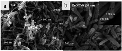 | ||
| Fig. 7 FESEM images of (a) ZnO nanorods and (b) CdS/ZnO nanorods (reprinted with permission from ref. 67, copyright 2012 American Chemical Society). | ||
| Sample | Shell thickness (nm) | Absorbance band (nm) | PL band (nm) | Current (A) | Photocatalytic efficiency (%) |
|---|---|---|---|---|---|
| ZnO | 372 | 380 | 9.22 × 10⁻⁷ | 70.0 | |
| ZnO/CdS1 | 10 | 425 | 460 | 8.09 × 10⁻⁶ | 85.0 |
| ZnO/CdS2 | 15 | 442 | 473 | 1.62 × 10⁻⁵ | 91.5 |
| ZnO/CdS3 | 30 | 465 | 490 | 1.75 × 10⁻⁵ | 98.0 |
2.5 Successive ionic layer adsorption and reaction
The “successive ionic layer adsorption and reaction” (SILAR) technique is another facile synthetic method to fabricate type-II core/shell heterostructures. This method was proposed by Nicolau68 in 1985. It is a heterogeneous chemical reaction at the solution–solid interface on which the cations and anions are absorbed. This reaction is as follows: m[CLp]n+ + n[AL′q]m− → CmAn↓ + mpL + nqL′. Here, L and L′ stand for different ligands and [CLp]n+and [AL′q]m− are cations and anions. After each immersion, the substrate with core/shell arrays should be rinsed by deionized water. The shell synthesized by SILAR can achieve better photoluminescence properties than those of shells synthesized by other methods.For example, Lee and Yong49 fabricated CuS nanoparticle/ZnO nanowire heterostructures on a mesh substrate. In this process, uniform CuS NPs were deposited on the pre-grown ZnO NWs array through SILAR. The synthesized CuS/ZnO heterostructured NWs exhibited superior photocatalytic activity under visible light illumination compared with that of the pure ZnO NWs. In addition, type-II heterostructured PbS/CdS p–n junctions have also been synthesized by successive cation exchange.69 Moreover, the photoelectrochemical activity of this structure could be tuned by changing the size and density of the PbS nanoparticles on the CdS nanowires. The morphology of this nanostructure is shown in Fig. 8.
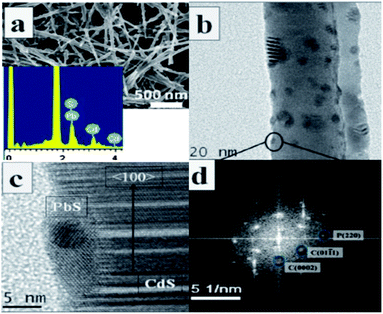 | ||
| Fig. 8 (a) SEM image of PbS/CdS synthesized by a cation exchange method, inset is EDX of the heterostructure. (b) TEM image showing a section of the nanowire with islands. (c) HRTEM indicating the presence of CdS and (d) FFT (SAED) pattern confirming the formation of PbS (reprinted with permission from ref. 69, copyright 2012 Royal Society of Chemistry). | ||
2.6 Solvothermal/hydrothermal method
The methods mentioned above are normally utilized to synthesize core/shell structures on substrates. For the preparation of powdery type II heterostructured photocatalysts, these methods are not the ideal choices due to the fact that powdery heterostructures are always dispersed in the solution. Solvothermal/hydrothermal methods, where the reaction occurs in a solvent, are one of the most commonly used preparation methods of powdery nanostructures.24,70–73 In a typical process, the mixture of a reagent such as amines and a precursor with appropriate ratio are injected in to a solvent which not only accelerates the dissolution of precursor but also speeds up the reaction rate between precursor and reagent with the increase of pressure and temperature. A pronounced advantage of this method is that most materials can be dissolved in appropriate solvent by modulating the temperature and pressure. In the case of the synthesis of AgIn5S8/TiO2 heterojunction nanocomposites,72 the mixture of TiO2, thioacetamide, AgNO3 and In(NO3)3·4.5H2O were dissolved in distilled water. After adjusting the pH value of the mixed solution to 10.2, it was then sealed in a Teflon-lined autoclave. Keeping the temperature at 180 °C for 24 h, the AgIn5S8/TiO2 heterojunction nanocomposite was precipitated. Interestingly, Yu and co-workers developed a microemulsion-mediated solvothermal synthetic method that simplifies the formation of CdS/TiO2 nanocomposites.24 In detail, titanium isopropoxide was first added into Millipore water (microemulsion A), and then Cd(NO3)2 (microemulsion B) and (NH4)2S (microemulsion C) were successively added in the mix solution. With simultaneous coprecipitation of Cd(NO3)2 and (NH4)2S in the water nanodroplets, CdS was coupled with TiO2 colloids.3 Photocatalysis properties and applications
During the past decades, various photocatalysts have been reported, such as TiO2, ZnO, WO3, ZnWO4, Bi2WO6, etc. The coupling of different semiconductors will result in improved photocatalytic activity. In type II heterostructure, excited electrons on the sensitizer semiconductor can transfer to the lower conduction band of the wide bandgap semiconductor, while holes are confined in sensitizer semiconductor, leading to an enhanced photocatalytic performance and an extended light absorption spectrum. Powdery photocatalysts have been a focus of great attention and development due to the high photocatalytic activity and relative simplicity of fabrication. However, powdery photocatalysts dispersed in solution agglomerate easily and are hard to separate from water. Recently, one-dimensional (1D) semiconductor nanostructures with type II core/shell structure grown on a substrate have made a profound impact on the application of photocatalysis. In this section, we review the photocatalytic properties of both powdery type II heterostructure photocatalysts and 1D type II core/shell structures grown on substrates based on very commonly used TiO2 and ZnO material systems. Some others photocatalysts like ZnWO4, Bi2WO6, α-Fe2O3, which have been intensively studied recently, are also presented. In particular, some type II structures which show high photocatalytic performance are highlighted.3.1 Powdery photocatalysts
Photocatalysts are widely used in powdery form due to the high photocatalytic activity and relative simplicity of fabrication. A wide bandgap semiconductor is usually coated with a narrow bandgap semiconductor to form a type II heterostructure. As a result, the photoinduced charge separation efficiency and the solar energy utilization of semiconductor are greatly improved. The morphology and geometry of heterostructure, surface texture, and particle size of the sensitizer play important roles in interface charge transfer and photocatalytic performance.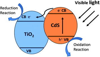 | ||
| Fig. 9 Schematic illustration of charge transfer in CdS/TiO2 heterostructure. | ||
Visible light generated electron transfer from CdS to TiO2 can not only enhance the charge separation efficiency but also extend the spectral response. Liu and co-workers prepared CdS/TiO2 semiconductor nanoparticles by microemulsion-mediated solvothermal hydrolyzation followed by acidic peptization of the precipitate. The photocatalytic activity of the CdS/TiO2 photocatalyst was confirmed by methylene blue (MB) degradation under visible light irradiation (λ > 420 nm).74 Yu and co-workers prepared nanosized CdS-sensitized TiO2 nanocrystals via a microemulsion-mediated solvothermal method.24 The morphologies of CdS/TiO2 are shown in Fig. 10a and b. Compared with pure TiO2, CdS/TiO2 nanocrystals exhibit enhanced efficiency for decomposition of methylene blue under visible light irradiation (Fig. 10c). Formation of Ti3+ on TiO2 under visible-light irradiation was demonstrated by electron paramagnetic resonance spectrum (EPR), indicating the effective photogenerated electron transfer from CB of CdS to that of TiO2. They also synthesized a CdSe/TiO2 heterostructured photocatalyst by an ultrasound-driven solution method.13 The CdSe/TiO2 heterostructured photocatalyst shows a higher photocatalytic activity than that of pure TiO2 in the degradation of 4-chlorophenol under visible light irradiation (λ > 400 nm). The quantum size effect of CdSe plays an important role in enhancing charge separation efficiency and photocatalytic activity of the CdSe/TiO2 heterostructured photocatalyst.13 Moreover, MoS2 and WS2 nanocluster sensitized TiO2 nanoparticles were synthesized via in situ photoreduction deposition by the same group.29 The quantum confinement effects of MoS2 and WS2 can cause an appropriate alternation in the energy levels of the conduction and valence band edges, making them suitable for the photosensitization of visible light in a coupled semiconductor system. Compared with pure TiO2, MoS2/TiO2 and WS2/TiO2 heterostructures show higher photocatalytic activity in MB and 4-chlorophenol degradation under visible light irradiation (λ > 400 nm).29 Besides the chalcogenides, there are various narrow bandgap semiconductors that can be coupled with TiO2 to form a type II heterostructure, enhancing photocatalytic performance and extending the light adsorption spectrum of TiO2, such as Ag2O,80,81 CuAlO2,82 LaVO4,28 AgIn5S8,83 V2O5.84
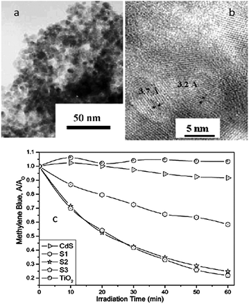 | ||
| Fig. 10 (a and b) TEM and HRTEM images of CdS/TiO2; (c) the MB degradation under visible light irradiation (660 nm) in the prepared photocatalysts (reprinted with permission from ref. 24, copyright 2003 Royal Society of Chemistry). | ||
In addition, type II heterostructures can combine with another material to form ternary hybrid catalysts. For example, TiO2 type II heterostructures usually combine with noble metals to enhance the photocatalytic activity in hydrogen production.85 In the CdS/TiO2/Pt system, the formation of the potential gradient at the interface between CdS and TiO2 and the Pt fabrication method play important roles in determining the hydrogen production efficiency.85
:1. It is worth pointing out that ZnO has low stability under long reaction times due to photocorrosion, and some effort has been devoted to inhibiting photocorrosion.
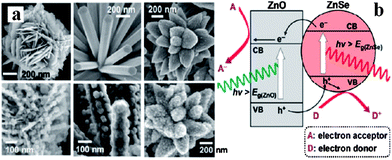 | ||
| Fig. 11 (a) SEM images of ZnO/ZnSe heterostructures; (b) schematic diagram showing the energy band structures of a ZnO/ZnSe heterostructure (reprinted with permission from ref. 90, copyright 2011 American Chemical Society). | ||
Zhu and co-workers fabricated a type II graphite-like C3N4/ZnO heterostructure.25 After coupling with C3N4, the photocurrent and photocatalytic activity of ZnO were both greatly enhanced under UV and visible light irradiation (Fig. 12a and b). Moreover, the photocorrosion of ZnO was successfully suppressed in the C3N4/ZnO heterostructure. The photocorrosion of ZnO is caused by photoinduced dissolution due to hole oxidation. Since the VB position of ZnO is lower than that of the C3N4, the photogenerated holes on ZnO could directly transfer to C3N4, leading to an effective photocorrosion inhibition (Fig. 12c). As shown in Fig. 12d, the visible photoactivity of C3N4/ZnO heterostructure originates from the injection of excited electrons from CB of C3N4 to the CB of ZnO.
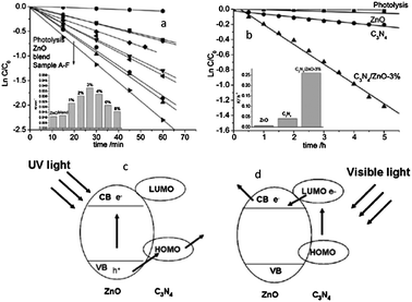 | ||
| Fig. 12 Photocatalytic degradation of MB over ZnO and C3N4/ZnO photocatalysts: (a) under UV light irradiation and (b) under visible light irradiation (visible light region in the range of 400–800 nm; the main wavelength is about 550 nm); schematic drawing illustrating the mechanism of charge separation of C3N4/ZnO photocatalyst: (c) under UV light irradiation and (d) under visible light irradiation (reprinted with permission from ref. 25, copyright 2011 Royal Society of Chemistry). | ||
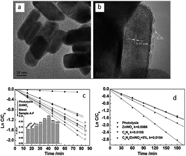 | ||
| Fig. 13 The morphology of ZnWO4 and C3N4/ZnWO4 photocatalysts: (a) ZnWO4 (b) C3N4/ZnWO4; pseudo-first-order rates of MB degradation over ZnWO4 and C3N4/ZnWO4 photocatalysts: (c) under UV light irradiation (λ = 254 nm) (d) under visible light irradiation (λ > 420 nm) (reprinted with permission from ref. 26, copyright 2012 Royal Society of Chemistry). | ||
3.2 1D type II core/shell photocatalysts
Compared with powder photocatalysts, one-dimensional (1D) semiconductor nanostructures with type II core/shell structures grown on substrates have made a profound impact on the application of photocatalysts because they effectively avoid agglomeration and possess a direct electrical pathway for the rapid transport of photogenerated carriers to the photoelectrode.102–104 The core is usually coated with a uniform shell and consequently a large interfacial area is formed in the interlayer, which ensures rapid charge separation. As a result, the nonradiative recombination of the electrons with electrolyte is inhibited and corrosion of core nanowires is prevented from electrolyte.105 Sometimes, the shell is substituted by quantum dots, which has been confirmed as a promising alternative to photosensitive dyes.106 They can produce multiple electron–hole pairs per photon and thus enhance the photoconversion efficiency.107Significantly, Yang and co-workers synthesized Z-scheme type CdS/Au/TiO2 hollow nanorod arrays (THNAs) on glass substrates by co-modifying TiO2 nanorods with Au and CdS nanoparticles.111 Ultraviolet-visible absorption spectra showed a red shift to 585 nm due to the strong electromagnetic coupling of Au and CdS compared with the pure TiO2 nanorod arrays and single Au or CdS nanoparticles. The CdS/Au/THNAs three-component nanojunction also exhibited enhanced photocatalytic activity. Using this kind of three-component nanojunction photocatalyst, the content of MB reduced by 72% after 2 h which is much more than that (15%) of pure THNAs under the same conditions.
Some ternary compounds are also used to modify TiO2 to get continuously adjustable spectral absorption by controlling the components. Park and co-workers reported that the TiO2 nanocable arrays coated by an Se-rich composition (CdS/CdSSe/CdSe multishell structures) showed excellent solar photocurrents and hydrogen generation rates.112 They also studied the photoelectric conversion efficiency of samples shelled with different compositions. It was confirmed that the CdS/CdSSe/CdSe multishell structures gained higher photoelectric conversion efficiency than that of CdSe and CdS.
In addition to TiO2 nanowire arrays, TiO2 nanotube arrays have also been used for type II band structures by decorating with CdS (ref. 113) and SrTiO3.114 Lin and co-workers used free-standing open-ended TiO2 nanotube membranes to degrade RhB, and then fabricated compound nanocables by stuffing the membrane with CdS.113Fig. 14 shows the setup used for flow-through photocatalysis experiments and the way in which the CdS is loaded. CdS/TiO2 nanocomposites show higher photocatalytic degradation activity compared with that of bare TiO2 nanotubes. The results suggest that the load of CdS increases light absorption of the CdS/TiO2 nanocomposites and, meanwhile, enhances the carrier separation efficiency. Furthermore, N and F codoped TiO2 nanotube arrays coupled with PbO nanoparticles showed significant enhancement on the photocatalytic degradation of organic pollutants due to the optoelectronic cooperation between TiO2 and PbO.115 Also, based on the same mechanism, this enhanced photocatalytic degradation has been realized with a CdSe nanoparticle-decorated TiO2 nanotube array.116
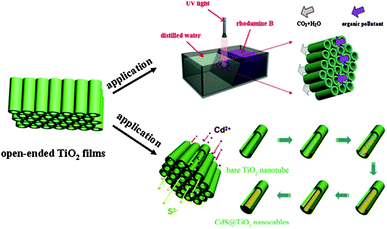 | ||
| Fig. 14 Schematic of applications of free-standing open-ended TiO2 nanotube membranes (reprinted with permission from ref. 113, copyright 2012 Elsevier). | ||
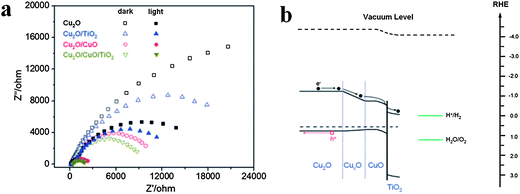
Furthermore, compared with single shell nanostructures, double-shell TiO2 nanostructures further improve photoelectrochemical (PEC) properties, as reported by Xiao and co-workers.117 Cu2O could absorb a wide range of visible light due to its narrow band gap (<2 eV), but it's difficult to use for water splitting due to its weak stability in solution. Xiao and co-workers prepared TiO2/CuO/Cu2O nanowire arrays on Au-coated copper substrates through controlled air annealing of the electrodeposited Cu nanowires and then dip coating with TiO2. The step-by-step enhancement of charge separation efficiency is indicated in the electrochemical impedance spectra (EIS) data in Fig.15a. Fig. 15b shows the energy band diagram of TiO2/CuO/Cu2O nanowire arrays and also the charge transfer route in electrolyte solution.
Recently, highly efficient photoelectrochemical hydrogen generation has been demonstrated on hierarchical WOx/ZnO nanowires by cosensitizing CdSe and CdS as shown in Fig. 16a.120 The support of the CdSe shell and CdS nanoparticles extended the light absorption of the WOx/ZnO nanowire array to a wavelength of 800 nm. A photocurrent density as high as 11 mA cm−2 at −0.5 V (vs. SCE) under 1.5 AM irradiation was achieved. This kind of enhanced light harvesting is obviously attributed to the synergy between WOx/ZnO and CdSe/CdS as well as the formation of type II core/shell structure. Fig. 16b and c show current density of CdSe/CdS/WOx/ZnO under chopped illumination.
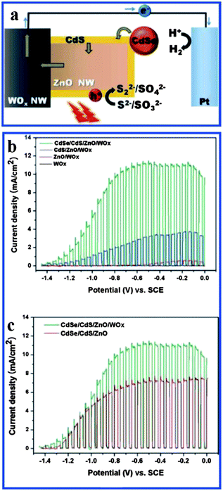 | ||
| Fig. 16 (a) Schematic of the photoelectrochemical hydrogen generation system based on CdSe/CdS/WOx/ZnO; (b) current density as a function of potential under chopped illumination (100 mW cm−2) of (black) as-prepared WOx nanowhiskers, (red) WOx/ZnO, (blue) CdS/WOx/ZnO, and (green) CdSe/CdS/WOx/ZnO; (c) comparison of J–E curves of CdSe/CdS/WOx/ZnO and CdSe/CdS/ZnO under chopped illumination (reprinted with permission from ref. 120, copyright 2011 American Chemical Society). | ||
In addition to quantum dots, a more commonly used decoration is the uniform nanoscale shell. For example, a ZnO nanowire array coated with a CdTe shell demonstrated a photocurrent density of ∼5.9 mA cm−2 under visible light illumination of 100 mW cm−2 at zero bias potential. The authors suggested that the favorable absorption of CdTe and the type II band alignment contributed to the excellent performance of this photoelectrode.48 Furthermore, our group recently successfully fabricated ZnSxSe1−x/ZnO core/shell nanowires via a two-step CVD method. The obtained core/shell structure showed a significant improvement of visible light absorption efficiency. It was explicitly demonstrated that the introduction of a ZnSxSe1−x shell to ZnO nanowires profoundly improved the photogenerated charge separation process.44
Based on the similar mechanism, there are also other 1D core/shell examples like CdSSe/ZnO.50 However, these works paid more attention to the manipulation of electronic structure. One method is to tailor the composition of the shell through controlling the synthetic process, and thus a tunable band gap can be achieved, which results in the continuous absorption of the solar spectrum. For example, ZnxCd1−xSe/ZnO core/shell nanowire arrays which were synthesized by temperature-gradient CVD yielded a continuous absorption edge from 2.7 to 1.77 eV across the sample surface by adjusting the Zn composition.35 This core/shell nanowire array showed photocurrent density of ∼5.6 mA cm−2 under 1 sun solar light illumination at zero bias versus Ag/AgCl. Another example is the ZnxCd1−xS/ZnO core/shell nanorod array whose shell also showed a tunable band gap from 2.52 to 3.11 eV.47 They exhibited a high photocatalytic activity and good stability in the degradation of the methylorange.
Another method is to change the element ratio of the intermediate layer so that exciton generation and separation were facilitated. For example, due to the formation of a CdZnSSe intermediate layer, CdSSe/ZnO core/shell nanowire showed higher photocurrent and hydrogen generation rate than that of CdS/TiO2 under AM 1.5 G conditions.50 The authors believe that Zn containing alloy layers in the interface region improved the epitaxial growth of single-crystalline shell layers on the ZnO nanowire core by the way of reducing the lattice mismatch and the number of defect sites.
Some other narrow band gap semiconductor materials, such as V2O5 whose band gap is 2.2 eV covering visible light range, have also been used to decorate ZnO.121 In the example of a V2O5-sensitized ZnO nanowire array, a ZnO nanowire array was first synthesized by a hydrothermal growth process, and then coated with V2O5 by magnetron sputtering. The absorption edge of the V2O5/ZnO core/shell structure was longer than that of pure ZnO nanowires. In addition, after annealing, the absorption of UV became weak while visible light absorption was enhanced due to the low diffusion of Zn atoms into the V2O5 layer. To further improve photoelectrochemical hydrogen generation, a double-shell structure such as CdSe/CdS has been used to decorate ZnO nanowire arrays.122 This fabrication lengthens the absorbance spectra of ZnO NWs array to 700 nm. The PEC performance of pure ZnO NWs, CdS/ZnO NWs, CdSe/CdS/ZnO NWs also demonstrated a step by step enhancement.
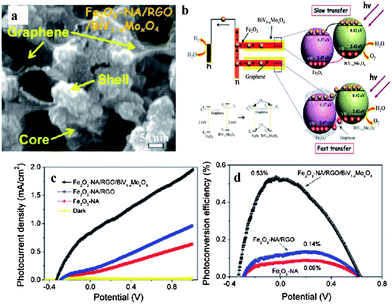 | ||
| Fig. 17 (a) Top SEM image of BiV1−xMoxO4/graphene/α-Fe2O3 core/shell; (b) schematic of energy band structure of BiV1−xMoxO4/graphene/α-Fe2O3 core/shell; (c) potential-dependent photocurrent density and (d) photoconversion efficiency as a function of applied potential of α-Fe2O3, RGO/α-Fe2O3, BiV1−xMoxO4/graphene/α-Fe2O3 (reprinted with permission from ref. 34, copyright 2012 American Chemical Society). | ||
In visible light driven photocatalytic systems, Si nanowire was also used as the core owing to its relatively high conduction band and valence band. Semiconductor materials with wide bandgap were used as the shell, such as TiO2,125,126 ZnO,127 ZnSe.128 As discussed in Xie's work, p-Si nanowires/TiO2 heterojunction arrays as the photocathode could utilize the visible light including wavelengths longer than 600 nm.125 They used p-Si as the under-layer to construct a p–n heterojunction with n-type TiO2 so that the semiconductors with narrow band gap could capture most of the sunlight photons to generate more photoelectrons for pollutant decomposition. The results show that the degradation efficiency of phenol reached 80.7% in 100 min under visible light owing to the synergy between the electrochemical process and the photocatalytic process. Later, Wang and co-workers demonstrated a mace-like core/shell three-dimensional (3D) nanorod network. In this network, the core array is composed of Si nanowires and the TiO2 nanorods were grown vertically on the frame.126 This unique structure gained a PEC efficiency of 2.1% which is three times higher than that of the TiO2 film/Si nanowire structure.
Based on a similar principle, Chen and co-workers obtained ZnO/Si core/shell nanowire arrays with about 8% optical reflectance in the visible region, which results in good optical absorption.127 They also studied the water splitting performance of ZnO/Si nanowire arrays. It was confirmed that the ZnO/Si core/shell nanowire arrays achieved higher photoconversion efficiency than that of the planar bilayer structure of ZnO/Si and the pure planar ZnO. In addition, p-type Si nanowire arrays coated with ZnSe nanoparticles also exhibited enhanced photodetection and photocatalytic performances.128
4 Conclusions
Photocatalysis appears to be a promising way to solve environmental and energy issues in the future. Over the past few decades, continuous breakthroughs in the synthesis, modification and application of semiconductors have been reported. In this review, we have described the general strategies and recent progress in the fabrication of type II heterostructures for environmental remediation and water splitting. We focus on synthetic methods and photocatalytic properties of TiO2 and ZnO based visible light driven type II 0D and 1D heterostructured photocatalysts. Some other low dimensional nanomaterials which showed high-performance photocatalysis are also presented, such as ZnWO4 nanoparticles, Bi2WO6 nanoparticles, α-Fe2O3 nanowire arrays and p-Si nanowire arrays. The formation of a type II heterostructure that integrates multiple functional components in the nanoscale significantly enhances the photocatalytic performance, which arises from: (1) the synergy of absorption between the core and the sensitizer; (2) type II heterostructures promote separation and transformation efficiency of photogenerated electron–hole pairs.It is worth noting that although great progress has achieved in the study of type II heterostructured photocatalysts, extensive application of type II heterostructured photocatalysts still faces several tough challenges: firstly, the quantum efficiency of type II heterostructures is still too low to utilize solar energy with high efficiency. Thus the dynamic behaviour of photogenerated carriers in the interface and surface of type II heterostructure needs to be further clarified so that researchers can design type II heterostructures rationally. Moreover, despite the successfully use of various synthetic methods to prepare type II nanoscale heterostructured photocatalysts, production by these methods is far from sufficient for industrial applications. In addition, type II heterostructured nanomaterials still suffer from chemical instability, which severely decreases the efficiency of the photocatalysts. Even the safety and the secondary pollution to the environment of nanoscale photocatalysts are still ambiguous. All in all, researchers all around the world need to carry out systematic and careful experimental studies and thus establish general and rational design guidelines in fabricating type II heterostructured nanoscale photocatalysts.
Acknowledgements
This work was supported by the 973 Program of Ministry of Science and Technology of China (no. 2012CB934103) and the 100-Talents Program of the Chinese Academy of Sciences (no. Y1172911ZX).Notes and references
- R. J. Cambell, China and the United States—A comparison of green energy programs and policies. Congressional Research Service. Report for Congress, Washington, DC, 2011 Search PubMed.
- A. Fujishima and K. Honda, Nature, 1972, 238, 37–38 CrossRef CAS.
- M. R. Hoffmann, S. T. Martin, W. Choi and D. W. Bahnemann, Chem. Rev., 1995, 95, 69–96 CrossRef CAS.
- H. Zhou, Y. Qu, T. Zeid and X. Duan, Energy Environ. Sci., 2012, 5, 6732–6743 CAS.
- I. K. Konstantinou and T. A. Albanis, Appl. Catal., B, 2004, 49, 1–14 CrossRef CAS.
- M. G. Walter, E. L. Warren, J. R. McKone, S. W. Boettcher, Q. Mi, E. A. Santori and N. S. Lewis, Chem. Rev., 2010, 110, 6446–6473 CrossRef CAS.
- A. Fujishima, T. N. Rao and D. A. Tryk, J. Photochem. Photobiol., C, 2000, 1, 1–21 CrossRef CAS.
- K. I. Hadjiivanov and D. G. Klissurski, Chem. Soc. Rev., 1996, 25, 61–69 RSC.
- A. Heller, Acc. Chem. Res., 1995, 28, 503–508 CrossRef CAS.
- H. Kominami, S. Murakami, J. Kato, Y. Kera and B. Ohtani, J. Phys. Chem. B, 2002, 106, 10501–10507 CrossRef CAS.
- J. C. Yu, L. Z. Zhang, Z. Zheng and J. C. Zhao, Chem. Mater., 2003, 15, 2280–2286 CrossRef CAS.
- R. Wang, G. Jiang, Y. Ding, Y. Wang, X. Sun, X. Wang and W. Chen, ACS Appl. Mater. Interfaces, 2011, 3, 4154–4158 CAS.
- W. Ho and J. C. Yu, J. Mol. Catal. A: Chem., 2006, 247, 268–274 CrossRef CAS.
- B. Kraeutler and A. J. Bard, J. Am. Chem. Soc., 1978, 100, 4317–4318 CrossRef CAS.
- V. Subramanian, E. E. Wolf and P. V. Kamat, J. Am. Chem. Soc., 2004, 126, 4943–4950 CrossRef CAS.
- R. Asahi, T. Morikawa, T. Ohwaki, K. Aoki and Y. Taga, Science, 2001, 293, 269–271 CrossRef CAS.
- P. V. Kamat, Pure Appl. Chem., 2002, 74, 1693–1706 CrossRef CAS.
- Y. Wang, R. Shi, J. Lin and Y. Zhu, Appl. Catal., B, 2010, 100, 179–183 CrossRef CAS.
- Y. Wang, J. Xu, W. Zong and Y. Zhu, J. Solid State Chem., 2011, 184, 1433–1438 CrossRef CAS.
- Y. Wang, J. Lin, R. Zong, J. He and Y. Zhu, J. Mol. Catal. A: Chem., 2011, 349, 13–19 CrossRef CAS.
- H. McDaniel, P. E. Heil, C. L. Tsai, K. K. Kim and M. Shim, ACS Nano, 2011, 5, 7677–7683 CrossRef CAS.
- M. Shim, H. McDaniel and N. Oh, J. Phys. Chem. Lett., 2011, 2, 2722–2727 CrossRef CAS.
- A. Kudo and Y. Miseki, Chem. Soc. Rev., 2009, 38, 253–278 RSC.
- J. C. Yu, L. Wu, J. Lin, P. Lia and Q. Li, Chem. Commun., 2003, 1552–1553 RSC.
- Y. Wang, R. Shi, J. Lin and Y. Zhu, Energy Environ. Sci., 2011, 4, 2922–2929 CAS.
- Y. Wang, Z. Wang, S. Muhammad and J. He, CrystEngComm, 2012, 14, 5065–5070 RSC.
- Y. Wang, X. Bai, C. Pan, J. He and Y. Zhu, J. Mater. Chem., 2012, 22, 11568–11573 RSC.
- H. Huang, D. Li, Q. Lin, W. Zhang, Y. Shao, Y. Chen, M. Sun and X. Fu, Environ. Sci. Technol., 2009, 43, 4164–4168 CrossRef CAS.
- W. Ho, J. C. Yu, J. Lin, J. Yu and P. Li, Langmuir, 2004, 20, 5865–5869 CrossRef CAS.
- Y. Tak, H. Kim, D. Lee and K. Yong, Chem. Commun., 2008, 4585–4587 RSC.
- Y. Tak, S. J. Hong, J. S. Lee and K. Yong, Cryst. Growth Des., 2009, 9, 2627–2632 CAS.
- H. M. Chen, C. K. Chen, Y. C. Chang, C. W. Tsai, R. S. Liu, S. F. Hu, W. S. Chang and K. H. Chen, Angew. Chem., 2010, 122, 6102–6105 CrossRef.
- J. Johansson and K. A. Dick, CrystEngComm, 2011, 13, 7175–7184 RSC.
- Y. Hou, F. Zuo, A. Dagg and P. Feng, Nano Lett., 2012, 12, 6464–6473 CrossRef CAS.
- H. Li, C. Cheng, X. Li, J. Liu, C. Guan, Y. Y. Tay and H. J. Fan, J. Phys. Chem. C, 2012, 116, 3802–3807 CAS.
- J. Li, M. W. G. Hoffmann, H. Shen, C. Fabrega, J. D. Prades, T. Andreu, F. Hernandez-Ramirezbc and S. Mathur, J. Mater. Chem., 2012, 22, 20472–20476 RSC.
- J. Luo, L. Ma, T. He, C. F. Ng, S. Wang, H. Sun and H. J. Fan, J. Phys. Chem. C, 2012, 116, 11956–11963 CAS.
- X. Wang, L. Yin, G. Liu, L. Wang, R. Saito, G. Q. M. Lu and H. M. Cheng, Energy Environ. Sci., 2011, 4, 3976–3979 CAS.
- X. Liu, C. Wang, X. Xu, J. Xu, X. Chen, X. Liu, R. Zou and H. Xing, CrystEngComm, 2013, 15, 1139–1145 RSC.
- S. Cho, J. W. Jang, J. S. Lee and K. H. Lee, Nanoscale, 2012, 4, 2066–2071 RSC.
- J. Schrier, D. O. Demchenko and L. W. Wang, Nano Lett., 2007, 7, 2377–2382 CrossRef CAS.
- Z. Yin, Z. Wang, Y. Du, X. Qi, Y. Huang, C. Xue and H. Zhang, Adv. Mater., 2012, 24, 5374–5378 CrossRef CAS.
- A. Kar, S. Kundu and A. Patra, RSC Adv., 2012, 10222–10230 RSC.
- Z. Wang, X. Zhan, Y. Wang, M. Safdar, M. Niu, J. Zhang, Y. Huang and J. He, Appl. Phys. Lett., 2012, 101, 073105 CrossRef.
- H. Jia, H. Xu, Y. Hu, Y. Tang and L. Zhang, Electrochem. Commun., 2007, 9, 354–360 CrossRef CAS.
- Z. Lu, J. Xu, X. Xie, H. Wang, C. Wang, S.-Y. Kwok, T. Wong, H. L. Kwong, I. Bello, C. S. Lee, S. T. Lee and W. Zhang, J. Phys. Chem. C, 2012, 116, 2656–2661 CAS.
- S. Xie, X. Lu, T. Zhai, J. Gan, W. Li, M. Xu, M. Yu, Y. M. Zhang and Y. Tong, Langmuir, 2012, 28, 10558–10564 CrossRef CAS.
- X. Wang, H. Zhu, Y. Xu and H. Wang, ACS Nano, 2010, 4, 3302–3308 CrossRef CAS.
- M. Lee and K. Yong, Nanotechnology, 2012, 23, 1–7 Search PubMed.
- Y. Myung, D. M. Jang, T. K. Sung, Y. J. Sohn, G. B. Jung, Y. J. Cho, H. S. Kim and J. Park, ACS Nano, 2010, 4, 3789–3800 CrossRef CAS.
- Z. Wang, H. Yin, C. Jiang, M. Safdar and J. He, Appl. Phys. Lett., 2012, 101, 253109 CrossRef.
- M. Zhong, Y. Li, I. Yamada and J. J. Delaunay, Nanoscale, 2012, 4, 1509–1514 RSC.
- M. Zhong, Y. Li, T. Tokizono, M. Zheng, I. Yamada and J. J. Delaunay, J. Nanopart. Res., 2012, 14, 804–814 CrossRef.
- H. Y. Chao, J. H. Cheng, J. Y. Lu, Y. H. Chang, C. L. Cheng and Y. F. Chen, Superlattices Microstruct., 2010, 47, 160–164 CrossRef CAS.
- R. S. Mane and C. D. Lokhande, Mater. Chem. Phys., 2000, 65, 1–31 CrossRef CAS.
- R. Ghosh Chaudhuri and S. Paria, Chem. Rev., 2011, 112, 2373–2433 CrossRef.
- X. Fang, T. Zhai, U. K. Gautam, L. Li, L. Wu, Y. Bando and D. Golberg, Prog. Mater. Sci., 2011, 56, 175–287 CrossRef CAS.
- A. Datta, S. K. Panda and S. Chaudhuri, J. Phys. Chem. C, 2007, 111, 17260–17264 CAS.
- S. Zhao, S. Chen, H. Yu and X. Quan, Sep. Purif. Technol., 2012, 99, 50–54 CrossRef CAS.
- C. Z. Yao, B. H. Wei, L. X. Meng, H. Li, Q. J. Gong, H. Sun, H. X. Ma and X. H. Hu, J. Power Sources, 2012, 207, 222–228 CrossRef CAS.
- B. Sun, Y. Z. Hao, F. Guo, Y. Cao, Y. Zhang, Y. Li and D. Xu, J. Phys. Chem. C, 2011, 116, 1395–1400 Search PubMed.
- X. Zhou, B. Jin, L. Li, F. Peng, H. Wang, H. Yub and Y. Fang, J. Mater. Chem., 2012, 22, 17900–17905 RSC.
- H. Wang, T. Wang, X. Wang, R. Liu, B. Wang, H. Wang, Y. Xu, J. Zhang and J. Duan, J. Mater. Chem., 2012, 22, 12532–12537 RSC.
- J. B. Wu, Z. G. Li, X. H. Huang and Y. Lin, J. Power Sources, 2013, 224, 1–5 CrossRef CAS.
- M. Y. Chen and Y. J. Hsu, Nanoscale, 2013, 5, 363–368 RSC.
- L. Dloczik and R. Konenkamp, Nano Lett., 2003, 3, 651–653 CrossRef CAS.
- S. Khanchandani, S. Kundu, A. Patra and A. K. Ganguli, J. Phys. Chem. C, 2012, 116, 23653–23662 CAS.
- Y. F. Nicolau, Appl. Surf. Sci., 1985, 22/23, 1061–1074 CrossRef.
- B. Mukherjee, A. Peterson and V. R. Subramanian, Chem. Commun., 2012, 48, 2415–2417 RSC.
- W. Ho and J. C. Yu, J. Mol. Catal. A: Chem., 2006, 247, 268–274 CrossRef CAS.
- M. T. Uddin, Y. Nicolas, C. L. Olivier, T. Toupance, L. Servant, M. M. Muller, H. Kleebe, J. Ziegler and W. Jaegermann, Inorg. Chem., 2012, 51, 7764–7773 CrossRef CAS.
- K. Li, B. Chai, T. Peng, J. Mao and L. Zan, ACS Catal., 2013, 3, 170–177 CrossRef CAS.
- A. Kar, S. Kundu and A. Patra, RSC Adv., 2012, 2, 10222–10230 RSC.
- J. Wang, Z. Liu, Q. Zheng, Z. He and R. Cai, Nanotechnology, 2006, 17, 4561–4566 CrossRef CAS.
- H. L. Meng, C. Cui, H. L. Shen, D. Y. Liang, Y. Z. Xue, P. G. Li and W. H. Tang, J. Alloys Compd., 2012, 527, 30–35 CrossRef CAS.
- A. Fujishima, X. Zhang and D. A. Tryk, Surf. Sci. Rep., 2008, 63, 515–582 CrossRef CAS.
- J. S. Jang, S. H. Choi, H. G. Kim and J. S. Lee, J. Phys. Chem. C, 2008, 112, 17200–17250 CAS.
- J. C. Yu, L. Wu, J. Lin, P. Li and Q. Li, Chem. Commun., 2003, 1552–1553 RSC.
- Y. Bessekhouad, D. Robert and J. V. Weber, J. Photochem. Photobiol., A, 2004, 163, 569–580 CrossRef CAS.
- W. Zhou, H. Liu, J. Wang, D. Liu, G. Du, S. Han, J. Lin and R. Wang, Phys. Chem. Chem. Phys., 2010, 12, 15119–15123 RSC.
- D. Sarkar, C. K. Ghosh, S. Mukherjee and K. K. Chattopadhyay, ACS Appl. Mater. Interfaces, 2012, 5, 331–337 Search PubMed.
- R. Brahimi, Y. Bessekhouad, A. Bouguelia and M. Trari, J. Photochem. Photobiol., A, 2007, 186, 242–247 CrossRef CAS.
- K. Li, B. Chai, T. Peng, J. Mao and L. Zan, ACS Catal., 2013, 3, 170–177 CrossRef CAS.
- Y. Wang, Y. R. Su, L. Qiao, L. X. Liu, Q. Su, C. Q. Zhu and X. Q. Liu, Nanotechnology, 2011, 22, 225702–225709 CrossRef CAS.
- H. Park, W. Choi and M. R. Hoffmann, J. Mater. Chem., 2008, 18, 2379 RSC.
- B. Dindar and S. Icli, J. Photochem. Photobiol., A, 2001, 140, 263–268 CrossRef CAS.
- C. Lizama, J. Freer, J. Baeza and H. D. Mansilla, Catal. Today, 2002, 76, 235–246 CrossRef CAS.
- A. A. Khodja, T. Sehili, J. Pilichowski and P. Boule, J. Photochem. Photobiol., A, 2001, 141, 231–239 CrossRef CAS.
- C. Ye, Y. Bando, G. Shen and D. Golberg, J. Phys. Chem. B, 2006, 110, 15146–15151 CrossRef CAS.
- S. Cho, J. W. Jang, J. Kim, J. S. Lee, W. Choi and K. H. Lee, Langmuir, 2011, 27, 10243–10250 CrossRef CAS.
- Z. Wang, B. Huang, Y. Dai, X. Qin, X. Zhang, P. Wang, H. Liu and J. Yu, J. Phys. Chem. C, 2009, 113, 4612–4617 CAS.
- J. S. Jang, J. Lee, H. Ye, F. F. Fan and A. J. Bard, J. Phys. Chem. C, 2009, 113, 6719–6724 CAS.
- L. Li, Y. Chu, Y. Liu and L. Dong, J. Phys. Chem. C, 2007, 111, 2123–2127 CAS.
- R. Abe, T. Takata, H. Sugihara and K. Domen, Chem. Commun., 2005, 3829–3831 RSC.
- A. Kudo and S. Hijii, Chem. Lett., 1999, 1103–1104 CrossRef CAS.
- R. Shi, Y. Wang, D. Li, J. Xu and Y. Zhu, Appl. Catal., B, 2010, 100, 173–178 CrossRef CAS.
- C. Pan and Y. Zhu, Environ. Sci. Technol., 2010, 44, 5570–5574 CrossRef CAS.
- C. Pan, J. Xu, Y. Wang, D. Li and Y. Zhu, Adv. Funct. Mater., 2012, 22, 1518–1524 CrossRef CAS.
- J. Yu and A. Kudo, Adv. Funct. Mater., 2006, 16, 2163–2169 CrossRef CAS.
- J. Ye, Z. Zou, M. Oshikiri, A. Matsushita, M. Shimoda, M. Imai and T. Shishido, Chem. Phys. Lett., 2002, 356, 221–226 CrossRef CAS.
- Z. Zhang, W. Wang, L. Wang and S. Sun, ACS Appl. Mater. Interfaces, 2012, 4, 593–597 CAS.
- L. J. Lauhon, M. S. Gudiksen, D. Wang and C. M. Lieber, Nature, 2002, 420, 57–61 CrossRef CAS.
- N. Skold, L. S. Karlsson, M. W. Larsson, M. E. Pistol, W. Seifert, J. Tragardh and L. Samuelson, Nano Lett., 2005, 5, 1943–1947 CrossRef.
- Y. Zhang, L. W. Wan and A. Mascarenhas, Nano Lett., 2007, 7, 1264–1269 CrossRef CAS.
- M. Seol, H. Kim, Y. Tak and K. Yong, Chem. Commun., 2010, 46, 5521–5523 RSC.
- A. J. Nozik, Physica E, 2002, 14, 115–120 CrossRef CAS.
- J. E. Murphy, M. C. Beard, A. G. Norman, S. P. Ahrenkiel, J. C. Johnson, P. Yu, O. I. Micic, A. J. Nozik, R. J. Ellingson and A. J. Nozik, J. Am. Chem. Soc., 2006, 128, 3241–3247 CrossRef CAS.
- H. Wang, Y. Bai, H. Zhang, Z. Zhang, J. Li and L. Guo, J. Phys. Chem. C, 2010, 114, 16451–16455 CAS.
- H. Wang, G. Wang, Y. Ling, M. Lepert, C. Wang, J. Z. Zhanga and Y. Li, Nanoscale, 2012, 4, 1463–1466 RSC.
- K. Shin, J. B. Yoob and J. H. Park, J. Power Sources, 2013, 225, 263–268 CrossRef CAS.
- H. Zhu, B. Yang, J. Xu, Z. Fu, M. Wen, T. Guo, S. Fu, J. Zuo and S. Zhang, Appl. Catal., B, 2009, 90, 463–469 CrossRef CAS.
- T. K. Sung, J. H. Kang, D. M. Jang, Y. Myung, G. B. Jung, H. S. Kim, C. S. Jung, Y. J. Cho, J. Park and C. L. Lee, J. Mater. Chem., 2011, 21, 4553–4561 RSC.
- J. Liao, S. Lin, N. Pan, D. Li, S. Li and J. Li, Chem. Eng. J., 2012, 211–212, 343–352 CrossRef CAS.
- X. Zhang, K. Huo, L. Hu, Z. Wu and P. K. Chuw, J. Am. Ceram. Soc., 2010, 93, 2771–2778 CrossRef CAS.
- Q. Li and J. K. Shang, Environ. Sci. Technol., 2010, 44, 3493–3499 CrossRef CAS.
- L. Yang, S. Luo, R. Liu, Q. Cai, Y. Xiao, S. Liu, F. Su and L. Wen, J. Phys. Chem. C, 2010, 114, 4783–4789 CAS.
- Q. Huang, F. Kang, H. Liu, Q. Lia and X. Xiao, J. Mater. Chem. A, 2013, 1, 2418–2425 CAS.
- M. a. Quintana, T. Edvinsson, A. Hagfeldt, G. Boschloo and T. Edvinsson, J. Phys. Chem. C, 2007, 111, 1035–1041 CAS.
- C. H. Hsu, C. H. Chen and D. H. Chen, J. Alloys Compd., 2013, 554, 45–50 CrossRef CAS.
- H. Kim, M. Seol, J. Lee and K. Yong, J. Phys. Chem. C, 2011, 115, 25429–25436 CAS.
- C. W. Zou, Y. F. Ra, A. Alyamani, W. Chu, M. J. Chen, D. A. Patterson, E. A. C. Emanuelsson and W. Gao, Langmuir, 2010, 26, 11615–11620 CrossRef CAS.
- M. Seol, H. Kim, W. Kim and K. Yong, Electrochem. Commun., 2010, 12, 1416–1418 CrossRef CAS.
- K. Sivula, F. L. Formal and M. Grtzel, ChemSusChem, 2011, 4, 432–449 CrossRef CAS.
- W. Wu, S. Zhang, X. Xiao, J. Zhou, F. Ren, L. Sun and C. Jiang, ACS Appl. Mater. Interfaces, 2012, 4, 3602–3609 CAS.
- H. Yu, X. Li, X. Quan, S. Chen and Y. Zhang, Environ. Sci. Technol., 2009, 43, 7849–7855 CrossRef CAS.
- J. Shi, Y. Hara, C. Sun, M. A. Anderson and X. Wang, Nano Lett., 2011, 11, 3413–3419 CrossRef CAS.
- M. Shi, X. Pan, W. Qiu, D. Zheng, M. Xu and H. Chen, Int. J. Hydrogen Energy, 2011, 36, 15153–15159 CrossRef CAS.
- Y. H. Chen, W. S. Li, C. Y. Liu, C. Y. Wang, Y. C. Chang and L. J. Chen, J. Mater. Chem. C, 2013, 1, 1345–1351 RSC.
| This journal is © The Royal Society of Chemistry 2013 |