
 Open Access Article
 This Open Access Article is licensed under a Creative Commons Attribution-Non Commercial 3.0 Unported Licence
Shelf lifetime analysis of organic solar cells combining frequency and time resolved techniques†
Alfonsina Abat Amelenan
Torimtubun
 *a,
Maria
Méndez
b,
José G.
Sánchez
b,
Josep
Pallarès
*a,
Emilio
Palomares
*bc and
Lluis F.
Marsal
*a
*a,
Maria
Méndez
b,
José G.
Sánchez
b,
Josep
Pallarès
*a,
Emilio
Palomares
*bc and
Lluis F.
Marsal
*a
aDepartment of Electric, Electronic and Automatic Engineering, Universitat Rovira I Virgili, 43007 Tarragona, Spain. E-mail: josep.pallares@urv.cat; lluis.marsal@urv.cat
bInstitute of Chemical Research of Catalonia (ICIQ-BIST), 43007 Tarragona, Spain. E-mail: epalomares@iciq.es
cCatalan Institution for Research and Advanced Studies (ICREA), 08010 Barcelona, Spain
First published on 15th November 2021
Abstract
The device operational lifetime and the understanding of the degradation pathways are critical steps for inverted organic solar cells (iOSCs) to enter the energy market. In this work, a combined study of impedance spectroscopy (IS) and photovoltage/photocurrent transient (TPV/TPC) techniques was employed to analyze the degradation of PTB7-Th:PC70BM-based iOSCs in accordance with the ISOS-D1 protocol under ambient conditions without encapsulation. Both techniques provide real information on how devices with different electron transport layers (PFN, TiOx, and ZnO) were degraded, affecting the stability of the active layer. We found that the main cause of degradation is the formation of interface traps in the dark and upon air exposure. The increase of trap density in the active layer upon degradation was revealed by TPV. The change in interface trap density due to the interfacial defect over the shelf-lifetime was further confirmed by the data from IS measurements. Last but not least, modelling dark current–voltage (J–V) using the IS data as well as the morphological changes of each ETL verified our hypothesis.
Introduction
Emerging photovoltaic technologies such as dye sensitized solar cells, perovskite solar cells, and organic solar cells have established their significance as sustainable solar to energy devices. Organic solar cells (OSCs), in contrast to current perovskite solar cells, are lead-free and low-cost with a short energy payback time, and can be solution processed on light-weight, semitransparent, flexible substrates over large areas by the roll-to-roll technique.1–5 Along with these appealing properties, in recent years, a rapid improvement in power conversion efficiency (PCE) up to over 18% in single-junction OSCs may endow OSCs with an opportunity to enter the market.6–8 However, high efficiency and low cost are not the only requirements to scale up OSC devices in the market. Device operational stability is also one of the key criteria to make the large-scale production of OSCs commercially more feasible. Up to now, silicon-based photovoltaic (PV) companies guarantee their products for 25 years of operational stability.9 For OSCs, a lifetime of over 20 years is estimated to be financially competitive,10 giving space for further device stability improvement.A huge effort is being made to understand the degradation mechanisms and strategies to make the OSC lifetime longer. For instance, modifying the chemical structure of the active layer materials, employing a ternary strategy for the active layer, using a compatibilizer to reduce the interfacial tension, inverting the OSC device polarity, optimizing buffer layers, using stable electrodes, eliminating the photo-dimerization of fullerenes, and increasing the material crystallinity of non-fullerene materials are known degradation mechanisms to minimize the intrinsic degradation.11–15 Meanwhile, a proper encapsulation is widely used to prevent the interaction of oxygen and moisture from the atmosphere with OSC devices. This method can lead to the suppression of the device extrinsic degradation. Nevertheless, the production cost, weight, and device flexibility are important concerns from the industrial engineering perspective when the devices need to be encapsulated. It is hence highly desirable to improve the intrinsic stability and minimize the encapsulation.
Some studies on polymer:fullerene OSCs showed that the inverted structure and the choice of the metal oxide, stable metal or electron transport polymer for the cathode material have a key contribution to improve the air stability of the device.16–18 In iOSCs, the use of hygroscopic and acidic poly(3,4-ethylenedioxythiophene):poly(styrene sulfonic acid) (PEDOT:PSS) can be avoided and the low work function aluminium electrode that causes the degradation can be replaced with a high work function metal electrode such as silver or gold.19 The electron transport layer (ETL) is a key component in acquiring high performance and stable iOSCs. The ETL has a role in modifying the alignment between the work function of the transparent conductive ITO cathode and the Fermi level of the semiconductor, promoting the electron transfer and the carrier extraction process.20,21 To improve the stability, the ETL may act as a scavenging layer to protect the active layer from oxygen and moisture.17 Transition metal oxides as ETLs, such as titanium dioxide (TiOx) and zinc oxide (ZnO), and water-soluble organic ETLs, poly[(9,9-bis(3′-(N,N-dimethylamino)propyl)-2,7-fluorene)-alt-2,7-(9,9-dioctylfluorene)] (PFN), are the most common ETLs used in iOSCs. These ETL materials exhibit high electron conductivity, an excellent optical transmittance, a low work function, a high refractive index, good chemical stability, non-toxicity, and an ability to improve charge carrier extraction.22–25
It is apparent that interlayer engineering and its optimization are the crucial factors to be considered to fabricate high performance and air-stable devices. To gain further insight into the physical mechanisms governing the device operation, optoelectronic characterization techniques are widely employed. Small-perturbation time- and frequency-domain measurements such as transient photovoltage/photocurrent (TPV/TPC) spectroscopy, charge extraction, and impedance spectroscopy (IS) have been widely employed to study relaxation processes in the field of dye-sensitized solar cells (DSSCs),26,27 OSCs,28,29 and perovskite solar cells,30 but fewer studies focused on the combination of both techniques. Electronic transitions can be studied with TPV/TPC on a very fast time scale (higher frequency), while the electronic and ionic conduction can be observed by IS on lower time scales (lower frequency).31 Nevertheless, the same information and comparable results can be obtained from TPV/TPC or EIS. Combined TPV and IS techniques have already been used by Pockett et al. to study the effect of degradation on the active layer and interlayer in OSCs.32 However, in-depth discussion of device lifetime analysis according to ISOS protocols using combined TPV and IS techniques remains unclear. In the meantime, ISOS protocols play an important role in the advancement of OSC's research and future industrial manufacture.
In this study, we perform IS and TPV/TPC measurements on an inverted PTB7-Th:PC70BM-based device with different ETL materials to investigate the effect of the ETL on the stability of nonencapsulated iOSCs. The standard procedure of the ISOS D-1 protocol (under dark and ambient conditions) was used for an accurate lifetime determination.33 Three different ETLs were investigated: one water-soluble organic-based (PFN) and two metal oxide-based (TiOx and ZnO). We demonstrate that TPV/TPC combined with IS can be employed to gain a deeper insight into the behavior and degradation mechanisms of iOSCs concerning the cathode interlayer used. The TPV measurements are useful in observing the degradation of the active layer as a result of trap formation, while the IS measurements give more detailed information about the interfacial density of states across the interlayer. We found that using an appropriate ETL can significantly improve the stability of iOSCs. Under nonencapsulated ambient conditions, metal oxides show a more stable ETL while organic interlayers are more susceptible to oxygen and moisture ingress.
Results & discussion
Photovoltaic characteristics obtained by current–density (J–V) measurements
In this study, bulk heterojunction (BHJ) devices were fabricated with an inverted configuration ITO/ETL/PTB7-Th:PC70BM/V2O5/Ag as schematically illustrated in Fig. 1a by using different ETL materials. An inverted structure is chosen to minimize any degradation originating from metal electrode oxidation and the acidic interfacial layer.34 The selected interlayers studied here represent the most common organic and inorganic materials employed as ETLs in iOSCs. The as-fabricated device namely “fresh device” was characterized immediately after the fabrication process. The nonencapsulated fresh devices were then kept in an ambient environment (room temperature (RT) of 23–27 °C and controlled relative humidity (RH) of 35–50%) under open circuit conditions with no illumination, following the ISOS-D1 protocol.33 The devices were only exposed to light during device characterization and returned to the dark shelf chamber.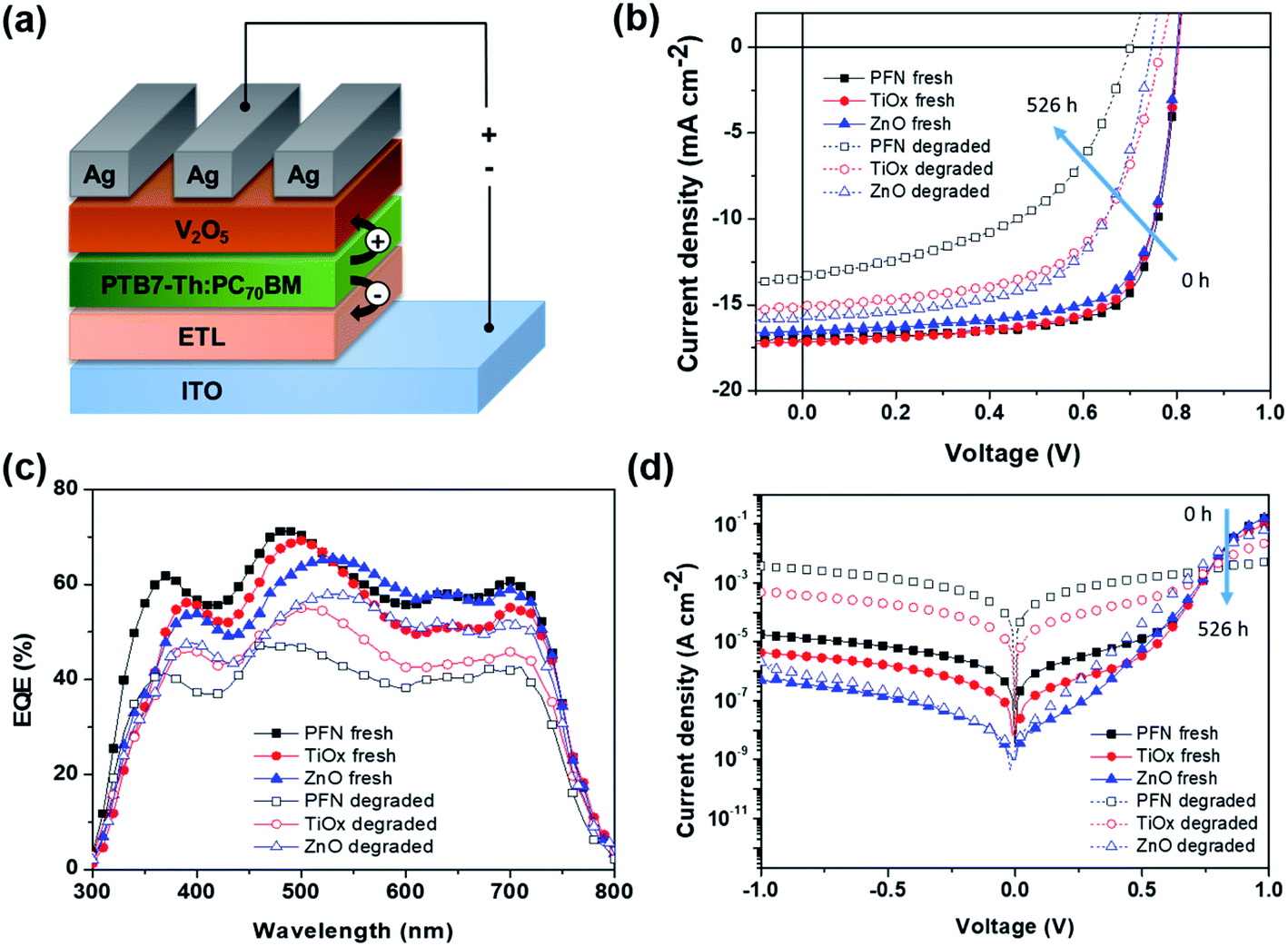 | ||
| Fig. 1 (a) Schematic illustration of the inverted device architecture, (b) J–V characteristics under illumination, (c) EQE spectra, and (d) dark J–V characteristics of fresh and 526 h degraded PTB7-Th:PC70BM-based devices with different ETLs (PFN, TiOx and ZnO). | ||
Fig. 1b shows the current density–voltage (J–V) characteristics of these fresh and degraded cells measured under simulated AM 1.5G illumination (100 mW cm−2) at RT. The corresponding device parameters are summarized in Table 1. In addition, Fig. S1a–c† show the initial transient of the illuminated J–V measurements. As for the performance of the fresh device, ZnO-iOSC shows the lowest JSC, the lowest shunt resistance (RSh), and thus the lowest PCEmax of 9.79%. TiOx-iOSC exhibits the highest JSC, the lowest FF and the highest series resistance (RS), resulting in a PCEmax of 9.99%. Meanwhile, PFN-iOSC can improve the device performance, showing the highest VOC, FF and RSh, which leads to the highest PCEmax of 10.35%. From the degradation perspective, degraded (526 h) devices show a prominent reduction in the device performance for all ETLs compared to the fresh (0 h) devices. The JSC of PFN-, TiOx-, and ZnO-iOSCs fell 13%, 9% and 7% after 526 h. The JSC reduction in all degraded cells is coherent with the reduction of calculated JSC values obtained from external quantum efficiency when compared to those of fresh devices, as shown in Fig. 1c. On the other hand, VOC decreases slightly after degradation, fell 10% for PFN-iOSC and fell 4% for each TiOx- and ZnO-iOSC. In addition, a significant decrease in FF after 526 h degradation is observed; FF fell by 33%, 17% and 16% for PFN-, TiOx- and ZnO-iOSCs, respectively. A significance FF reduction may arise from a gradual increase of RS and a drop of RSh is observed for degraded devices as a result of the parasitic resistance effect. It leads to a considerably lower PCE, where the PCE of PFN-iOSC drops to almost 50% of its initial value while those of TiOx- and ZnO-iOSCs drop to 26% and 24% from their initial value. In general, the devices using PFN as the cathode interlayer in iOSCs suffer from the worst stability, while the devices using ZnO as the ETL resulted in the most stable devices. Since the device architecture and fabrication process are identical, the difference in device parameter stability observed may be attributed to the different ETL materials used.
| ETL | J SC (Jcalc)a [mA cm−2] | V OC [V] | FF [%] | PCE (PCEmax) [%] | R S [Ω cm2] | R Sh [Ω cm2] | |
|---|---|---|---|---|---|---|---|
| a The Jcalc is the integrated current density calculated from the EQE spectra. | |||||||
| PFN | Fresh | 16.83 ± 0.37 (15.98) | 0.80 ± 0.006 | 74.40 ± 0.52 | 10.00 ± 0.20 (10.35) | 0.95 ± 0.06 | 1618 ± 542 |
| Degraded | 14.69 ± 0.93 (14.04) | 0.71 ± 0.018 | 50.21 ± 1.22 | 5.31 ± 0.36 (5.89) | 7.94 ± 1.08 | 242 ± 23 | |
| TiOx | Fresh | 17.19 ± 0.17 (16.71) | 0.79 ± 0.005 | 71.40 ± 1.12 | 9.73 ± 0.18 (9.99) | 1.69 ± 0.08 | 1044 ± 315 |
| Degraded | 15.71 ± 0.39 (15.01) | 0.76 ± 0.004 | 59.43 ± 1.62 | 7.11 ± 0.32 (7.39) | 5.16 ± 2.04 | 543 ± 63 | |
| ZnO | Fresh | 16.70 ± 0.20 (15.43) | 0.79 ± 0.005 | 72.45 ± 0.61 | 9.60 ± 0.14 (9.79) | 0.94 ± 0.07 | 858 ± 424 |
| Degraded | 15.53 ± 0.32 (14.47) | 0.76 ± 0.017 | 61.17 ± 1.86 | 7.21 ± 0.25 (7.41) | 2.78 ± 1.27 | 531 ± 132 | |
Fig. 1d further compares the dark J–V characteristics of all devices before and after 526 hours of degradation. Table S1† summarizes the experimental and modeled device performance parameters from dark J–V curves. The fitting values are obtained using a two-diode equivalent model, where the detailed fitting calculation can be found elsewhere.35 In addition, Fig. S1d–f† show the initial transient of the dark J–V measurements and Fig. S2† displays the fitting for the fresh and degraded devices. All fresh devices show an ideal exponential region with an ideality factor in the range of 1.05 to 1.11, combined with RS at medium–high voltage bias and a leakage current at low bias, which can be linked to the manufacturing imperfections.36 The leakage current depends on the ETL and can be ascribed to the combination of a RSh and a second non-ideal exponential region with an ideality factor larger than 2. A high leakage current is probably caused by lower contact selectivity within the cell and higher surface energy when aged in the presence of water and oxygen.37,38 After 526 h degradation, all devices show a reduction in the current density in forward and reverse biases due to the loss in diode and resistance properties. The observed RS increment in all degraded devices can be ascribed to several factors such as the creation of deep and shallow traps due to the interaction of oxygen and water with the polymer reducing charge carrier mobility, a loss of injection efficiency from the electrode contact into the active layer due to increasing barrier for charge injection or the creation of an isolation layer between the bulk active layer and contact hindering the charge carrier collection.39 In addition, the ideality factor values of the degraded devices in the first exponential region change to 1.59–1.91 and the leakage current strongly increases due to the reduction of RSh values and the worsening of the second exponential region, with ideality factors much larger than 2. Therefore, the lower PCE observed in PFN-iOSC and TiOx-iOSC than those of ZnO-iOSC could be due to lower charge extraction and higher leakage current. Therefore, the lower PCE observed in PFN-iOSC and TiOx-iOSC than those of ZnO-iOSC could be due to lower charge extraction and higher leakage current, which are limiting factors that correlated with the higher trap defects upon degradation, as described later in this work.
To get a further insight into the degradation trend behavior of iOSCs with different ETLs over shelf lifetime in an ambient environment, the normalized device performance parameters (VOC, JSC, FF and PCE) are presented in Fig. 2. Corresponding to the ISOS-D1 protocol, the operating shelf lifetime of each studied cell is summarized in Table 2. The term E0 is the initial testing measurement of fresh devices at 0 h (T0), while E80 is the testing measurement of degraded devices under dark ambient conditions after the PCE decays 20% from its initial value at time T80.33Fig. 2a shows the PCE decay behavior of all devices. It is worth noting that rapid PCE decay in the first few hours is observed in all devices. It is known as the “burn-in loss” degradation loss mechanism due to the photochemical reaction within the device layers.40,41 It can be seen that PFN-iOSC degraded to 80% of its initial PCE (T80) after only 26 h, faster than its TiOx- and ZnO-iOSC counterparts that took 341 h (2 weeks) and 526 h (3 weeks) to reach T80, suggesting the poor stability of PFN as the ETL in nonencapsulated iOSCs. It is because their performance parameter decreases rapidly in a short exposure time, as shown in Fig. 2b and Table 2. The VOC, JSC, and FF of PFN-iOSC at T80 are reduced down to 4%, 6% and 16%, while those of TiOx-iOSC at T80 fall to 3%, 7%, and 11% (Fig. 2c) and those of ZnO-iOSC at T80 are decreased down to 5%, 8%, and 14% (Fig. 2d), respectively. The evolution of illuminated and dark J–V characteristics over the device lifetimes is shown in Fig. S1.† In general, compared to the other device parameters, VOC seems to be the least affected by the degradation in PTB7-Th:PC70BM-based iOSCs, while JSC and FF appear to suffer more by the degradation. It suggests that the performance deterioration is probably more associated with the charge extraction and leakage current-dominated photogeneration, which is correlated with the interlayer quality of the devices.
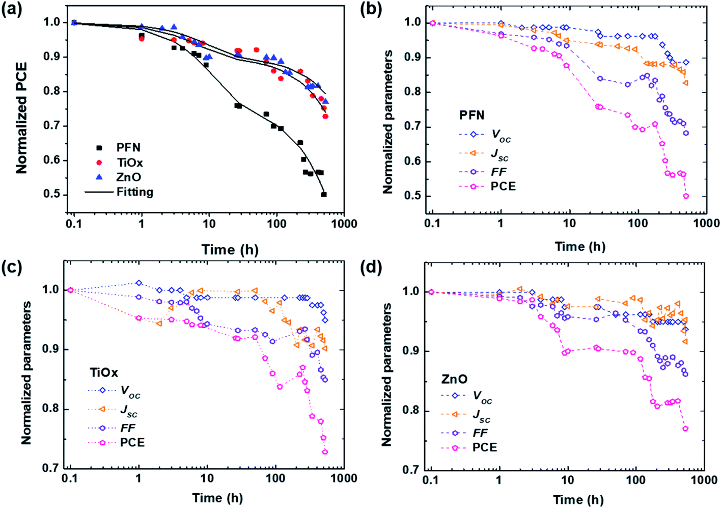 | ||
| Fig. 2 (a) Fitting of the normalized PCE over the storage time using eqn (1) for all devices. (b)–(d) Normalized device performance parameters of each inverted PTB7-Th:PC70BM-based device with different ETLs: (b) PFN, (c) TiOx, and (d) ZnO. The symbols are the experimental data, the solid lines are the fitting curves, and the dashed lines are guide to the eyes. The samples were degraded in dark ambient environment and all measurements were carried out under AM 1.5G illumination. | ||
| Standard lifetime | PFN | TiOx | ZnO |
|---|---|---|---|
| E 0, T0 (PCE, %) | 10.35 | 9.99 | 9.79 |
| T 95 | 3 | 8 | 7 |
| T 90 | 9 | 70 | 115 |
| T 85 | 12 | 224 | 224 |
| T 80 | 26 | 341 | 526 |
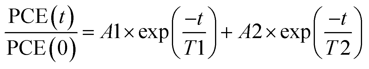
As displayed in Fig. 2a, the degradation of all devices displays an exponential decay. A fast initial decay followed by a slow decay can be fitted by the superposition of two exponential functions with different time constants, as previously reported:18,42
 | (1) |
Fig. 3 presents the behaviour of series and shunt resistances over shelf lifetime. As shown in Fig. 3a, the RS of nonencapsulated iOSCs with different ETLs increases after 526 h exposure to ambient conditions in which the decay behaviour of RS is observed similarly with the PCE decay behavior in Fig. 2a. RS values keep constant from its initial time and start to increase at 3 h (T95), 70 h (T90), and 115 h (T90) for PFN-, TiOx- and ZnO-iOSCs, respectively. Afterwards, RS values rise abruptly for PFN-, increase gradually for TiOx- and increase steadily for ZnO-iOSCs until 526 h. Interestingly, in Fig. 3b, it is shown that the RSh of ZnO-iOSC was stable for 526 h, while those of PFN- and TiOx-iOSCs showed a rapid decrease for 26 h (T80) and 70 h (T90), respectively, following the PCE decay behaviour. The most stable and the lowest RS combined with the highest RSh values belong to ZnO-iOSC which is coherent with FF and PCE decay behaviour (see Fig. 2 and Table S2†). As the increase of RS and decrease of RSh are followed by the FF and PCE decay, it is reasonable to suppose that the stability of the studied iOSCs exposed to ambient conditions is related to interface degradation, as observed in similar work.43,44 This is in good agreement with the AFM measurement of each ETL fresh and degraded film, as shown in Fig. S4.† The difference between the root-mean-square (RMS) roughness of fresh and degraded ZnO films is very small (ΔRMS = 0.01 nm) compared to the PFN film (ΔRMS = 1.31 nm), which indicates an effective interfacial area between the ZnO layer and the active layer. The smoother the ETL film, the smaller the ETL/active layer interfacial area and the fewer the interface traps, leading to suppressed undesired charge recombination and leakage current, which reduces the FF.45,46 This can be attributed to the function of the ZnO layer as a scavenging layer to prevent the diffusion of oxygen and water molecule ingress to the active layer.17 Moreover, a better quality ZnO film than the other ETLs can help to passivate the blend/ETL interface layer from the interface defect due to the chemisorption of oxygen as trap states causing the concentration of free electrons to decrease.47,48 Nevertheless, it is important to note that due to the complexity of the degradation mechanisms of each layer within the device, the information extracted solely from the J–V characteristics does not provide conclusive evidence to understand the dominating mechanism of performance deterioration. Therefore, a combined technique of time and frequency domains to perform shelf-lifetime degradation analysis is discussed more in detail in the following section.
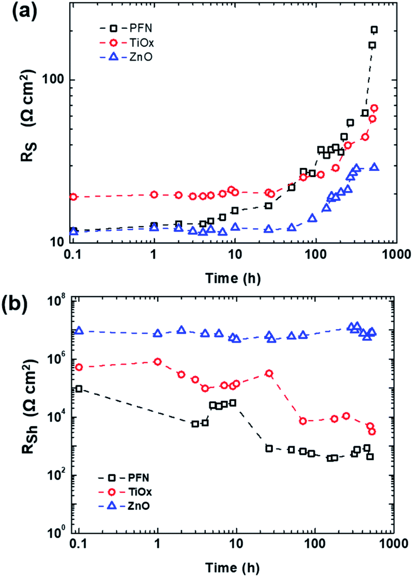 | ||
| Fig. 3 (a) Series and (b) shunt resistances of the inverted PTB7-Th:PC70BM-based device over shelf lifetime with different ETLs (PFN, TiOx and ZnO) extracted from dark J–V measurements. | ||
Transient photovoltage (TPV)/photocurrent (TPC) analysis
To investigate the effect of different ETLs on charge kinetics and recombination, fresh and degraded nonencapsulated iOSCs were measured under operando conditions by using charge extraction (CE) and transient photovoltage (TPV)/photocurrent (TPC) techniques. These techniques have been frequently employed to analyze the carrier losses and the carrier recombination in dye-sensitized solar cells and OSCs,49–51 and more recently in perovskite solar cells.52–54 Understanding the carrier loss mechanisms is key to increase solar cell efficiency. Therefore, we consider analyzing fresh and degraded devices as an important way to elucidate the different mechanisms at the device interfaces. While a brief description of the experimental procedure can be found in the Device characterization section, the technique is described in detail elsewhere.55In general, the CE technique allows the measurement of accumulated charges and the TPV enables the study of carrier recombination decay under different light biases (solar cell voltage as a result of light irradiation). In most kinds of solar cells, such as full-organic or dye-sensitized solar cells, photo-generated carriers are extracted before they recombine. In other words, the CE decay is always much faster than the TPV at the same light bias, as we can observe from our devices (see Fig. S5†). Nevertheless, the combination of TPV/TPC allows obtaining the differential capacitance (DC) as an alternative technique to CE.56 Here we used both CE and DC techniques to accurately analyse the charge density of the devices (see an example in Fig. S6†).
For a comparison between iOSCs with different ETLs, we made sure that the film thicknesses are equal in all devices within the measurement error, i.e. ETL thicknesses close to 20 nm. Fig. 4a shows photo-generated charges stored in the fresh and degraded cells at equilibrium at different VOC values, achieved by tuning the background illumination from the dark to 1 Sun equivalent. At first sight, the degraded samples showed higher charge density values for a given VOC. In agreement with similar work recently reported,32 this can be attributed to chemical reactions as a result of interlayer degradation originating near the interface. Meanwhile, the charge density for the fresh devices is very similar for the different ETLs and consistent with the observed VOC (∼0.8 V), and the increase in charge density upon degradation is different for each ETL and so less consistent with the VOC. Charge density usually exhibited a linear and exponential part, attributed to the charges accumulated at the interfaces – known as geometrical capacitance – and within the bulk – chemical capacitance–, as depicted in Fig. S7.† By analyzing both separately, we obtained more information about how the degradation process affects the charge extraction of the devices depending on the ETL used. Fig. S7b† shows that TiOx in degraded cells presents slightly higher charge density.
 | ||
| Fig. 4 (a) The charge density vs. VOC and (b) the charge lifetime vs. charge density for fresh and degraded devices. | ||
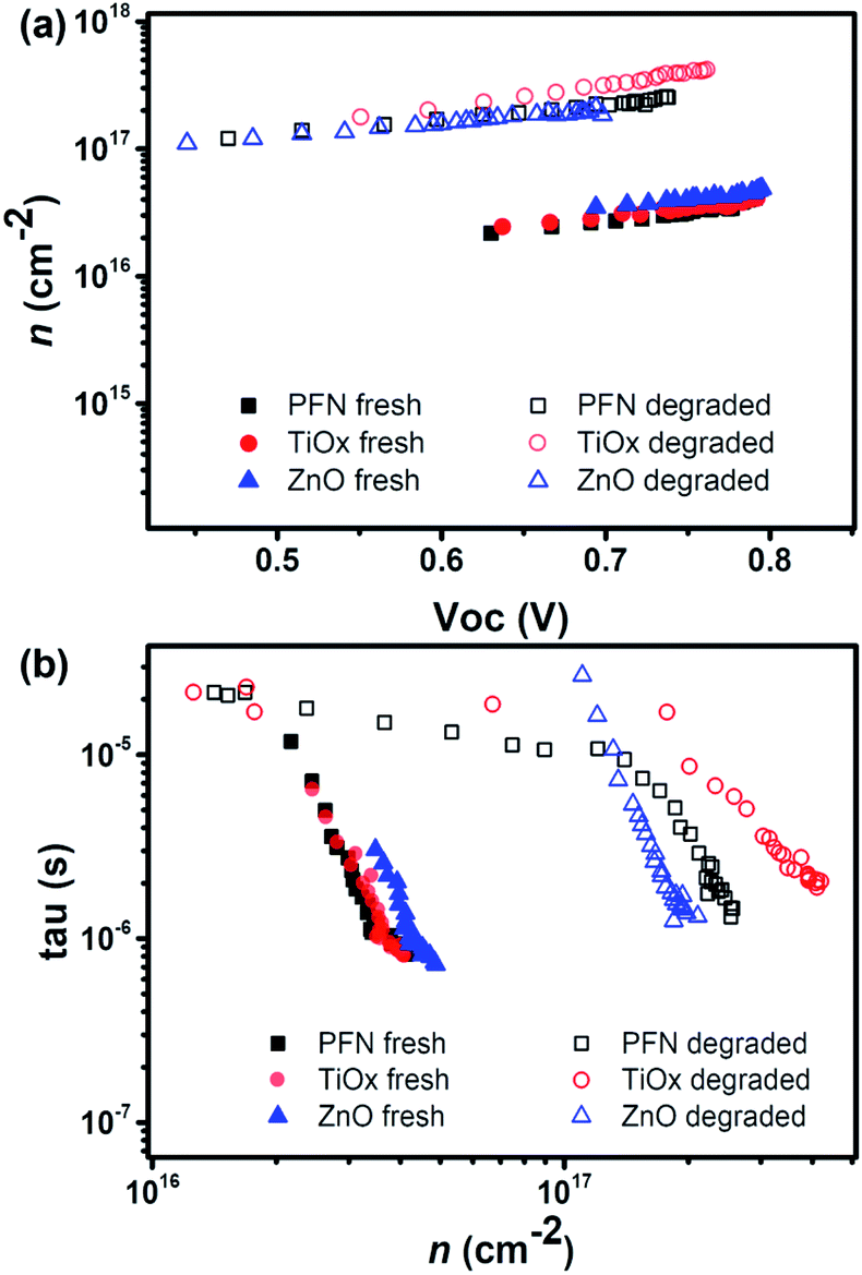
A change in recombination kinetics can be observed by looking at the charge density dependence of the carrier lifetime. Therefore, the carrier lifetimes (τ) obtained from the TPV decays of fresh and degraded devices are plotted as a function of charge density in Fig. 4b. There is an improvement in the carrier lifetime in the degraded devices, approximately 3 times longer than the fresh devices at a charge density of 2.5 × 1016 cm−2.
These results are consistent with the increase in trap formation upon degradation (mainly due to oxygen and water penetration) as carrier lifetimes are shown to increase for given carrier densities. Due to the presence of traps, charges may spend a certain amount of time in these traps, before being released and so being recombined. We have seen that the increased carrier lifetime does not causes higher VOC values for those degraded devices because to reach the same Fermi-level splitting, much higher charge density would now be needed compared to the fresh devices. We can also notice that, in general, lifetimes are similar for all devices, especially close to 1 Sun intensity, which indicates that the ETL properties do not have a significant influence on recombination kinetics.
Therefore, we can conclude from this section that, as we have not observed significant changes in recombination behavior and in the device ideality factor from light intensity dependency measurement (see Fig. S8†), the observed performance degradation is improbable to come from energy level changes. In this case, we can confirm that the degradation does not induce significant increases in trap-assisted recombination which may be one potential source of performance loss.
Impedance spectroscopy analysis
To obtain a deeper understanding of the degradation mechanism associated with the interfaces, we performed IS measurements on the same devices investigated by TPV/TPC. IS measures the phase shift and the amplitude of the current response obtained upon applying an AC voltage to the device at a given frequency. The frequency dependent measurements aid to explain the several mechanisms occurring at several interfaces.57 Thus, the interface state will be distinguished more easily by IS than by TPV, in which all charges are forced to recombine.The first approach to fit the experimental IS data of all fresh samples is to use an equivalent circuit model comprising one series resistance connected in series with three resistor/capacitor components (3RC). The 3RC equivalent circuit model can be employed to get information about each layer within the devices.58,59 To properly fit the impedance data at higher frequencies (HFs), i.e. f > 0.1 MHz, for all fresh samples, the main effect to overcome is the reduction of the phase values. From the circuital point of view, a reduction of the −Z′′ experimental value on the negative x-axis can only be explained by the presence of series inductance (L). The physical origin of the L term could be related to wiring, although compensation was done before the measurement. An alternative origin could be the typical equivalent circuit of a capacitor at HF. A series resistance element (RS) takes into consideration the ITO sheet resistance and three RC elements correspond to the capacitance and resistance of the ETL, the bulk active layer, and the hole transport layer (HTL). The geometrical capacitance (Cgeo) values of each layer are listed in Table S3.† These values depend on the dielectric permittivity and the thickness of the layer, as expressed by eqn (S1).† The comparison of the different Cgeo values of each layer and the fitting values enables us to predict the correlation between RC components.
The typical arc behavior with a single semi-circle is observed in the Cole–Cole plots (Fig. 5a) with one peak in the phase angle of Bode plots (Fig. 5b), suggesting the presence of RC components. Table S4† summarizes the extracted capacitance and resistance values from fitting the impedance spectra of all devices using the 3RC equivalent circuit model under open-circuit conditions. It is noticed that ITO sheet resistances depend on the ETL used, where a RS value in the range of 10 Ω was expected. Among the fresh samples, at a given frequency, PFN-iOSCs demonstrate the lowest impedance value in the flat region of |Z| vs. f compared to the metal oxide-ETL counterparts. These results corroborate the highest device performance obtained using PFN-ETL as the fresh device. It is worth noting that the fitted equivalent capacitance values (Cfit) of the bulk are higher than the Cgeo of the blend by ≈3 nF. From the circuital point of view, an increase of Cfit compared to Cgeo can only be explained by the presence of a parallel capacitance. Fig. S9† shows the equivalent circuit model used to fit the impedance spectra, allowing the interfacial density of states (Dit) of the blend and the traps created during the degradation process to be observed. This estimation is based on polymer metal–insulator–semiconductor (MIS) capacitor work.60,61 The interface states are represented by an interface trap capacitance (Cit) in parallel with the capacitance of the semiconductor. Cit can be obtained by subtracting Cgeo from Cfit (Cit = Cfit − Cgeo), so the interface density of states Dit = Cit/qA can be calculated as 4–6 × 1011 cm−2 eV−1 for PTB7-Th under open-circuit conditions, see Table 3. These values are within the range of values obtained for the interface density of states in P3HT.62,63
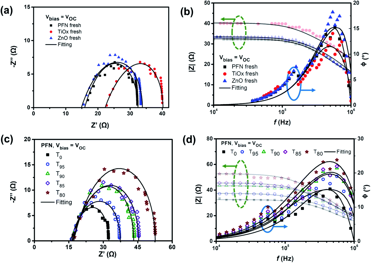 | ||
| Fig. 5 (a) and (c) Cole–Cole plot and (b) and (d) Bode plot (modulus green-dashed arrow and phase blue-solid arrow) for (a) and (b) fresh devices using three different ETLs and (c) and (d) degraded PFN-based non-encapsulated devices over degradation time (T0, T95, T90, T85, and T80) measured under open-circuit conditions. The experimental results were fitted using a RC circuit model (solid lines) shown in Fig. S9.† | ||
| ETL | C it = Cfit − Cgeo (nF) | D it = Cit/QA (cm−2 eV−1) | ΔDit (%) | ||
|---|---|---|---|---|---|
| Fresh | Degraded | Fresh | Degraded | ||
| PFN | 7 | 11 | 4.86 × 10¹¹ | 7.64 × 10¹¹ | 57 |
| TiOx | 6 | 9 | 4.17 × 10¹¹ | 6.25 × 10¹¹ | 50 |
| ZnO | 9 | 10 | 6.25 × 10¹¹ | 6.94 × 10¹¹ | 11 |
After degradation, as shown in Fig. 5c, a single semicircle behavior is still observed with the increased average diameter of the arcs over storage time for PFN-iOSCs under open-circuit conditions. A similar trend is observed for the other studied ETLs. The time degradation impedance characteristics have been examined by fitting these with an equivalent circuit model. Another common characteristic for PFN-, TiOx- and ZnO-iOSCs is that the diameter of arcs decreases with increasing applied bias voltage, which can be related to the efficient charge extraction.58Fig. 5d exhibits the |Z|–f relation of PFN-iOSC over degradation time in which the impedance values increase as the degradation time increases and the difference is more prominent in the lower frequencies (LF) region, suggesting that the LF feature becomes evident in the degraded cells. As compared to Cgeo values, the fitted capacitance values of charge transport layers (ETL and HTL) appear to be the same and remain constant during degradation, see Table S4.† However, the fitted capacitance values of the blend in all samples are higher than those of geometrical values and their values increase with the degradation time. As shown in Table 3, the interface density of states values after a degradation time of 526 hours increases by 57%, 50% and 11% for PFN-, TiOx- and ZnO-iOSCs, respectively, in good agreement with the increase of the dark leakage current–voltage characteristic in the degraded devices. The highest degradation of the PFN iOSC correlates with the largest increase of the interface density of states values for this sample. Thus, we can assume that the traps created by water and oxygen will modify only the bulk interface with the ETL and HTL, whereas the ETL and HTL are fully depleted layers.
Combined steady-state and transient techniques
To obtain an excellent agreement within the steady-state and transient techniques, we compare both the ideality factors obtained from dark J–V modelling results with TPV/TPC studies. As shown in Fig. 6, the charge carrier density and charge carrier lifetime both exponentially depend on VOC, following eqn (2) and (3): | (2) |
 | (3) |
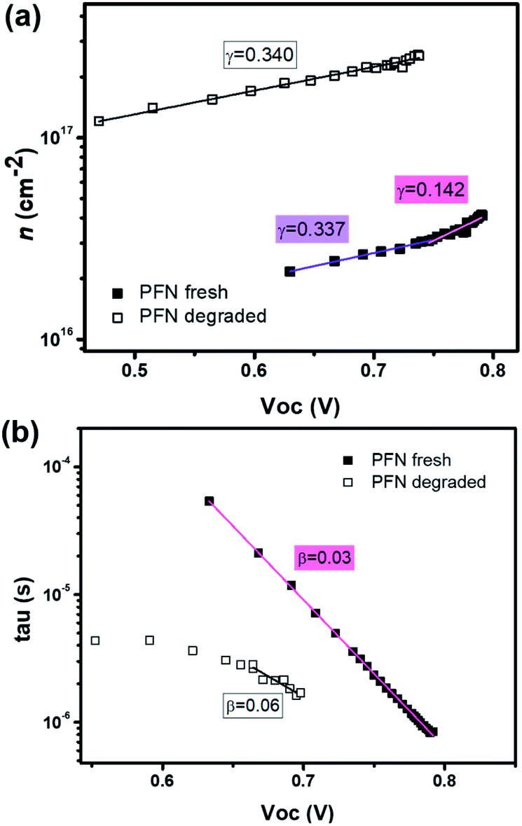 | ||
| Fig. 6 The fitted data of (a) charge carrier density and (b) charge carrier lifetime versus open circuit voltage from CE and TPV measurements using eqn (2) and (3) for the fresh and degraded PFN-iOSCs. | ||
| n n | n τ | n id (CEnn/TPVnτ) | n id (J–V) | |
|---|---|---|---|---|
| PFN fresh | 5.48 (VOC > 0.75) | 1.42 | 1.12 | 1.11 |
| 13.01 (VOC < 0.75) | — | — | ||
| PFN deg. | 13.13 | 2.31 | 1.96 | 1.91 |
Charge extraction and transient photovoltage techniques can be used to determine not only charge carrier densities and carrier recombination but also steady-state parameters like the ideality factor nid. The diode ideality factor is correlated with nn (at higher VOC voltages, i.e. 0.75–0.79 V) and nτ by following eqn (4):
| n−1id = n−1n + n−1τ | (4) |
Although the ideality factors were determined in two different ways – from J–V characteristics and from CE and TPV techniques – both nid found to be identical for our solar cells. These nid values have already been compared by other authors,64,66,67 where they obtained identical ideality factors as in our case, very close values or slightly underestimated compared to the steady-state values. Therefore, the good agreement of steady-state and transient techniques demonstrates the validity of the Shockley model for this kind of solar cell.
To validate the aforementioned assumption and the proposed model of Dit, we checked the time constant obtained from the IS and TPV measurements. The similar carrier lifetime values between the two techniques should correlate with each other when the recombination took place. The characteristic time constant from the RC circuit of IS data under open-circuit conditions is given by τ = R × C. The time constants measured from both techniques for PFN-iOSCs are shown in Fig. 7. On one side, each VOC bias point from IS data corresponds to a different degradation time with the same illumination, whereas on the other side those of TPV data correspond to the same degradation time with different illumination. A good agreement is observed between the total τ of IS in the VOC range from 0.8 V (fresh sample) to 0.74 V (degraded sample 176 h) and the total τ of TPV fresh PFN-iOSCs data from 0.8 V (the highest light intensity) to 0.74 V (lower light intensity). The time constant obtained from IS in the VOC range from 0.74 V to 0.70 V (degraded 526 h) mismatched the pattern of TPV fresh and follow the pattern of TPV degraded data. To determine which layer is the primary cause of shelf degradation, we analyze the contribution of each layer. We found that by fitting the ETL time constant, τETL = RETL × CETL, it follows the trend of τ extracted from TPV for degraded devices at 267 h and 526 h. The relative τ contribution of each layer to the total τ is shown in Fig. S10.† In fresh devices, almost 30% contribution of τ values is due to the HTL, whereas in the degraded devices, almost 70% contribution of τ values is due to the ETL. This result is in good agreement with the generation of interfacial traps in the degradation process. It suggests that the interfacial defects, demonstrated by the presence of the interface state effect, Dit, can be the main cause of degradation.
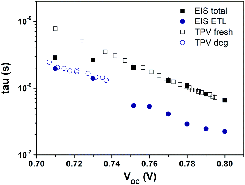 | ||
| Fig. 7 IS time constant under open-circuit conditions compared to the carrier lifetimes extracted from TPV measurements for the fresh and degraded PFN-iOSCs. | ||
Conclusions
In summary, we performed both frequency and time-domain characterization techniques to investigate the shelf-life degradation of ITO/ETL/PTB7-Th:PC70BM/V2O5/Ag using three different ETLs, one organic-based ETL (PFN) and two metal oxide-based ETLs (TiOx and ZnO), following the ISOS-D1 protocol. Both techniques can provide real information on how different ETLs were degraded, affecting the stability of the active layer over storage time. We have found that the main cause of degradation is the formation of interface traps in the r dark and upon air exposure. TPV measurements give an insight into the interfacial recombination processes, and particularly they show an increase of trap density in the active layer due to the degradation. From the IS data, it is possible not only to determine the relative contribution of each layer to the total time constant but also to estimate the increase of the interface density of states values due to the degradation process. Modelling dark current–voltage (J–V) characteristic and atomic force microscopy (AFM) measurements further confirm the presence of traps in the degraded devices.Conflicts of interest
The authors declare that there is no conflict of interest.Acknowledgements
A. A. A. T. acknowledges the financial support from the European Union's Horizon 2020 research and innovation programme under the Marie Skłodowska-Curie grant agreement No. 713679. This work was further supported by the Spanish Ministerio de Ciencia, Innovación y Universidades (MICINN/FEDER) RTI2018-094040-B-I00, by the Agency for Management of University and Research Grants (AGAUR) ref. 2017-SGR-1527, by Diputació de Tarragona 2021CM14 and from the Catalan Institution for Research and Advanced Studies (ICREA) under the ICREA Academia Award. ICIQ and ICREA are also acknowledge for its contribution with the transient photo-induced measurements and discussion of the results.References
- B. Zhao, Z. He, X. Cheng, D. Qin, M. Yun, M. Wang, X. Huang, J. Wu, H. Wu and Y. Cao, J. Mater. Chem. C, 2014, 2, 5077–5082 RSC.
- A. Gusain, R. M. Faria and P. B. Miranda, Front. Chem., 2019, 7, 1–25 Search PubMed.
- V. I. Madogni, B. Kounouhéwa, A. Akpo, M. Agbomahéna, S. A. Hounkpatin and C. N. Awanou, Chem. Phys. Lett., 2015, 640, 201–214 CrossRef CAS.
- Z. Hu, J. Wang, X. Ma, J. Gao, C. Xu, X. Wang, X. Zhang, Z. Wang and F. Zhang, J. Mater. Chem. A, 2021, 9, 6797–6804 RSC.
- Y. Wang, F. Wang, J. Gao, Y. Yan, X. Wang, X. Wang, C. Xu, X. Ma, J. Zhang and F. Zhang, J. Mater. Chem. C, 2021, 9, 9892–9898 RSC.
- Y. Lin, B. Adilbekova, Y. Firdaus, E. Yengel, H. Faber, M. Sajjad, X. Zheng, E. Yarali, A. Seitkhan, O. M. Bakr, A. El-Labban, U. Schwingenschlögl, V. Tung, I. McCulloch, F. Laquai and T. D. Anthopoulos, Adv. Mater., 2019, 1902965, 1902965 CrossRef PubMed.
- Y. Lin, Y. Firdaus, M. I. Nugraha, F. Liu, S. Karuthedath, A. Emwas, W. Zhang, A. Seitkhan, M. Neophytou, H. Faber, E. Yengel, I. Mcculloch, L. Tsetseris, F. Laquai and T. D. Anthopoulos, Adv. Sci., 2020, 1903419, 1–9 Search PubMed.
- Q. Liu, Y. Jiang, K. Jin, J. Qin, J. Xu, W. Li, J. Xiong and J. Liu, Sci. Bull., 2020, 65, 272–275 CrossRef CAS.
- W. R. Mateker and M. D. McGehee, Adv. Mater., 2017, 1603940, 1–16 Search PubMed.
- X. Xu, J. Xiao, G. Zhang, L. Wei, X. Jiao, H. L. Yip and Y. Cao, Sci. Bull., 2020, 65, 208–216 CrossRef CAS.
- M. J. Newman, E. M. Speller, J. Barbé, J. Luke, M. Li, Z. Wang, S. M. Jain, J. Kim, H. Ka, H. Lee, M. J. Newman, E. M. Speller, J. Barbé, J. Luke, M. Li, Z. Wang, S. M. Jain, J. Kim, H. Ka, H. Lee and W. C. Tsoi, Sci. Technol. Adv. Mater., 2018, 6996, 1–9 Search PubMed.
- A. A. A. Torimtubun, J. Follana-Berná, J. G. Sánchez, J. Pallarès, Á. Sastre-Santos and L. F. Marsal, ACS Appl. Energy Mater., 2021, 4, 5201–5211 CrossRef CAS.
- P. Cheng and X. Zhan, Chem. Soc. Rev., 2016, 45, 2544–2582 RSC.
- L. Duan and A. Uddin, Adv. Sci., 2020, 1903259, 1–39 Search PubMed.
- Q. An, F. Zhang, W. Gao, Q. Sun, M. Zhang, C. Yang and J. Zhang, Nano Energy, 2018, 45, 177–183 CrossRef CAS.
- B. Ecker, J. C. Nolasco, J. Pallarés, L. F. Marsal, J. Posdorfer, J. Parisi and E. Von Hauff, Adv. Funct. Mater., 2011, 21, 2705–2711 CrossRef CAS.
- J. G. Sánchez, V. S. Balderrama, M. Estrada, E. Osorio, J. Ferré-Borrull, L. F. Marsal and J. Pallarès, Sol. Energy, 2017, 150, 147–155 CrossRef.
- V. S. Balderrama, M. Estrada, P. L. Han, P. Granero, J. Pallarés, J. Ferré-Borrull and L. F. Marsal, Sol. Energy Mater. Sol. Cells, 2014, 125, 155–163 CrossRef CAS.
- I. I. Jeon and Y. Matsuo, Sol. Energy Mater. Sol. Cells, 2015, 140, 335–343 CrossRef CAS.
- Y. Wang, H. Cong, B. Yu, Z. Zhang and X. Zhan, Materials, 2017, 10, 1064 CrossRef PubMed.
- A. A. A. Torimtubun, J. G. Sanchez, J. Pallares and L. F. Marsal, in 2020 IEEE Latin America Electron Devices Conference (LAEDC), IEEE, San Jose, Costa Rica, 2020, pp. 1–4 Search PubMed.
- D. Yang, P. Fu, F. Zhang, N. Wang, J. Zhang and C. Li, J. Mater. Chem. A, 2014, 2, 17281–17285 RSC.
- M. Prosa, M. Tessarolo, M. Bolognesi, O. Margeat, D. Gedefaw, M. Gaceur, C. Videlot-Ackermann, M. R. Andersson, M. Muccini, M. Seri and J. Ackermann, ACS Appl. Mater. Interfaces, 2016, 8, 1635–1643 CrossRef CAS PubMed.
- F. X. Xie, W. C. H. Choy, W. E. I. Sha, D. Zhang, S. Zhang, X. Li, C. W. Leung and J. Hou, Energy Environ. Sci., 2013, 6, 3372–3379 RSC.
- A. A. A. Torimtubun, J. G. Sánchez, J. Pallarès and L. F. Marsal, Sustainable Energy Fuels, 2020, 4, 3378–3387 RSC.
- A. Sacco, Renewable Sustainable Energy Rev., 2017, 79, 814–829 CrossRef CAS.
- W. Yan, M. M. Huo, R. Hu and Y. Wang, RSC Adv., 2019, 9, 1734–1740 RSC.
- M. Jiang, H. R. Bai, H. F. Zhi, J. K. Sun, J. L. Wang, F. Zhang and Q. An, ACS Energy Lett., 2021, 6, 2898–2906 CrossRef CAS.
- M. Jiang, H. Bai, H. Zhi, L. Yan, H. Y. Woo, L. Tong, J. Wang, F. Zhang and Q. An, Energy Environ. Sci., 2021, 14, 3945–3953 RSC.
- J. Jiménez-López and E. Palomares, Nanoscale, 2019, 11, 20024–20029 RSC.
- E. Von Hauff, J. Phys. Chem. C, 2019, 123, 11329–11346 CrossRef CAS.
- A. Pockett, H. K. H. Lee, B. L. Coles, W. C. Tsoi and M. J. Carnie, Nanoscale, 2019, 11, 10872–10883 RSC.
- M. O. Reese, S. A. Gevorgyan, M. Jørgensen, E. Bundgaard, S. R. Kurtz, D. S. Ginley, D. C. Olson, M. T. Lloyd, P. Morvillo, E. A. Katz, A. Elschner, O. Haillant, T. R. Currier, V. Shrotriya, M. Hermenau, M. Riede, K. R. Kirov, G. Trimmel, T. Rath, O. Inganäs, F. Zhang, M. Andersson, K. Tvingstedt, M. Lira-Cantu, D. Laird, C. McGuiness, S. Gowrisanker, M. Pannone, M. Xiao, J. Hauch, R. Steim, D. M. Delongchamp, R. Rösch, H. Hoppe, N. Espinosa, A. Urbina, G. Yaman-Uzunoglu, J. B. Bonekamp, A. J. J. M. Van Breemen, C. Girotto, E. Voroshazi and F. C. Krebs, Sol. Energy Mater. Sol. Cells, 2011, 95, 1253–1267 CrossRef CAS.
- N. Chaturvedi, S. Kumar Swami, A. Kumar and V. Dutta, Sol. Energy Mater. Sol. Cells, 2014, 126, 74–82 CrossRef CAS.
- J. Pallarès, R. Cabré, L. F. Marsal and R. E. I. Schropp, J. Appl. Phys., 2006, 100, 2–7 CrossRef.
- N. Grossiord, J. M. Kroon, R. Andriessen and P. W. M. Blom, Org. Electron., 2012, 13, 432–456 CrossRef CAS.
- A. Guerrero, N. F. Montcada, J. Ajuria, I. Etxebarria, R. Pacios, G. Garcia-Belmonte and E. Palomares, J. Mater. Chem. A, 2013, 1, 12345–12354 RSC.
- M. A. Islam, M. Hasanuzzaman and N. A. Rahim, IEEE Journal of Photovoltaics, 2018, 8, 1259–1265 Search PubMed.
- K. Kawano, R. Pacios, D. Poplavskyy, J. Nelson, D. D. C. Bradley and J. R. Durrant, Sol. Energy Mater. Sol. Cells, 2006, 90, 3520–3530 CrossRef CAS.
- A. Sacramento, V. S. Balderrama, M. Ramírez-como, L. F. Marsal and M. Estrada, Sol. Energy, 2020, 198, 419–426 CrossRef CAS.
- J. Kong, S. Song, M. Yoo, G. Y. Lee, O. Kwon, J. K. Park, H. Back, G. Kim, S. H. Lee, H. Suh and K. Lee, Nat. Commun., 2014, 5, 1–8 Search PubMed.
- H. Bin Yang, Q. L. Song, C. Gong and C. M. Li, Sol. Energy Mater. Sol. Cells, 2010, 94, 846–849 CrossRef.
- K. Norrman, M. V. Madsen, S. A. Gevorgyan and F. C. Krebs, J. Am. Chem. Soc., 2010, 132, 16883–16892 CrossRef CAS PubMed.
- A. Guerrero, M. Pfannmöller, A. Kovalenko, T. S. Ripolles, H. Heidari, S. Bals, L. D. Kaufmann, J. Bisquert and G. Garcia-Belmonte, Org. Electron., 2015, 16, 227–233 CrossRef CAS.
- Z. Ma, Z. Tang, E. Wang, M. R. Andersson, O. Inganäs and F. Zhang, J. Phys. Chem. C, 2012, 116, 24462–24468 CrossRef CAS.
- B. Qi and J. Wang, Phys. Chem. Chem. Phys., 2013, 15, 8972–8982 RSC.
- M. R. Lilliedal, A. J. Medford, M. V. Madsen, K. Norrman and F. C. Krebs, Sol. Energy Mater. Sol. Cells, 2010, 94, 2018–2031 CrossRef CAS.
- M. Ramírez-Como, A. Sacramento, J. G. Sánchez, M. Estrada, J. Pallarès, V. S. Balderrama and L. F. Marsal, Sol. Energy Mater. Sol. Cells, 2021, 230, 111265 CrossRef.
- L. Xu, C. Aumaitre, Y. Kervella, G. Lapertot, C. Rodríguez-seco, E. Palomares, R. Demadrille and P. Reiss, Adv. Funct. Mater., 2018, 1706291 CrossRef.
- V. S. Balderrama, J. G. Sánchez, G. Lastra, W. Cambarau, S. Arias, J. Pallarès, E. Palomares, M. Estrada and L. F. Marsal, J. Mater. Chem. A, 2018, 6, 22534–22544 RSC.
- S. M. Tuladhar, M. Azzouzi, F. Delval, J. Yao, A. A. Y. Guilbert, T. Kirchartz, N. F. Montcada, R. Dominguez, F. Langa, E. Palomares and J. Nelson, ACS Energy Lett., 2016, 1, 302–308 CrossRef CAS.
- C. Rodríguez-Seco, M. Méndez, C. Roldán-Carmona, R. Pudi, M. K. Nazeeruddin and E. J. Palomares, Angew. Chem., Int. Ed., 2020, 1–6 Search PubMed.
- N. Y. Nia, M. Méndez, A. Di Carlo and E. Palomares, Philos. Trans. R. Soc., A, 2019, 377, 1–8 Search PubMed.
- N. F. Montcada, M. Méndez, K. T. Cho, M. K. Nazeeruddin and E. Palomares, Nanoscale, 2018, 10, 6155–6158 RSC.
- E. Palomares, N. F. Montcada, M. Méndez, J. Jiménez-López, W. Yang and G. Boschloo, in Characterization Techniques for Perovskite Solar Cell Materials, 2019, pp. 161–180 Search PubMed.
- A. Maurano, C. G. Shuttle, R. Hamilton, A. M. Ballantyne, J. Nelson, W. Zhang, M. Heeney and J. R. Durrant, J. Phys. Chem. C, 2011, 115, 5947–5957 CrossRef CAS.
- S. K. Gupta, L. S. Pali and A. Garg, Sol. Energy, 2019, 178, 133–141 CrossRef CAS.
- E. Osorio, J. G. Sánchez, L. N. Acquaroli, M. Pacio, J. Ferré-Borrull, J. Pallarès and L. F. Marsal, ACS Omega, 2017, 2, 3091–3097 CrossRef CAS PubMed.
- A. A. A. Torimtubun, J. G. Sanchez, J. Pallares and L. F. Marsal, IEEE J. Electron Devices Soc., 2021, 9, 484–491 CAS.
- I. Torres and D. M. Taylor, J. Appl. Phys., 2005, 98, 073710 CrossRef.
- H. Hirwa, S. Pittner and V. Wagner, Org. Electron., 2015, 24, 303–314 CrossRef CAS.
- C. M. Proctor, C. Kim, D. Neher and T. Q. Nguyen, Adv. Funct. Mater., 2013, 23, 3584–3594 CrossRef CAS.
- A. Foertig, J. Kniepert, M. Gluecker, T. Brenner, V. Dyakonov, D. Neher and C. Deibel, Adv. Funct. Mater., 2014, 24, 1306–1311 CrossRef CAS.
- A. Foertig, J. Rauh, V. Dyakonov and C. Deibel, Phys. Rev. B: Condens. Matter Mater. Phys., 2012, 86, 1–7 CrossRef.
- C. G. Shuttle, B. O'Regan, A. M. Ballantyne, J. Nelson, D. D. C. Bradley, J. De Mello and J. R. Durrant, Appl. Phys. Lett., 2008, 92, 1–4 CrossRef.
- D. Kiermasch, L. Gil-Escrig, A. Baumann, H. J. Bolink, V. Dyakonov and K. Tvingstedt, J. Mater. Chem. A, 2019, 7, 14712–14722 RSC.
- T. Kirchartz, B. E. Pieters, J. Kirkpatrick, U. Rau and J. Nelson, Phys. Rev. B: Condens. Matter Mater. Phys., 2011, 83, 1–13 CrossRef.
Footnote |
| † Electronic supplementary information (ESI) available: Experimental section, dark J–V fitting, modelled normalized PCE, AFM, CE and DC techniques, JSC and VOCvs. light intensity, capacitance & resistance values and IS data. See DOI: 10.1039/d1se01107c |
| This journal is © The Royal Society of Chemistry 2021 |