
Sb2S3 solar cells: functional layer preparation and device performance
Qian
Wang
ab,
Zhu
Chen
ac,
Jianyue
Wang
ac,
Yinyan
Xu
ab,
Yaping
Wei
ab,
Yuhan
Wei
*d,
Longzhen
Qiu
 a,
Hongbo
Lu
a,
Yunsheng
Ding
b and
Jun
Zhu
*a
a,
Hongbo
Lu
a,
Yunsheng
Ding
b and
Jun
Zhu
*a
aNational Engineering Lab of Special Display Technology, State Key Lab of Advanced Display Technology, Academy of Opto-Electronic Technology, Hefei University of Technology, Hefei, 230009, China. E-mail: jzhu@hfut.edu.cn
bAnhui Provincial Key Laboratory of Advance Functional Materials and Devices, School of Chemistry and Chemical Engineering, Hefei University of Technology, Hefei, 230009, China
cSchool of Electronic Science and Applied Physics, Hefei University of Technology, Hefei, 230009, China
dKey Laboratory of Biobased Polymer Materials, Shandong Provincial Education Department, College of Polymer Science and Engineering, Qingdao University of Science and Technology, Qingdao, 266042, China. E-mail: weiyh@qust.edu.cn
First published on 27th September 2019
Abstract
Photovoltaic power generation, as a rapidly growing new energy source, is a technology that uses a semiconductor to convert light energy into electrical energy. Sb2S3 solar cells possess the advantages of simple binary components, abundant resources, nontoxicity, and excellent stability; they have recently attracted extensive investigation interest. Various strategies, such as solution and vacuum deposition, have been used to fabricate functional layers, including Sb2S3 photoactive layers, electron transport layers and hole transport layers. Here, we briefly review the preparation methodologies, morphologies, structures, optoelectronic properties and the corresponding solar cell performance of functional layers for both planar heterojunction solar cells and mesoporous sensitized solar cells. Some viewpoints of further improvement of Sb2S3 solar cell conversion efficiency from the aspect of material fabrication and modification are given.
 Qian Wang | Qian Wang received her bachelor's degree from Anhui Jianzhu University in 2010 and her master's degree from China University of Mining and Technology in 2013. After that, she worked as a lecturer at Liupanshui Normal University until 2018. She is currently a Ph.D. candidate under the supervision of Prof. Jun Zhu at Hefei University of Technology. Her research interests focus on the design and fabrication of novel solar cells. |
 Zhu Chen | Zhu Chen received his bachelor's degree from Hefei University in 2018. Currently, he is a master's student at the Hefei University of Technology. His research interests focus on the preparation of perovskite solar cells. |
 Yuhan Wei | Yuhan Wei received her Ph.D. degree in 2009 from Changchun Institute of Applied Chemistry, Chinese Academy of Sciences. Then, she worked as a postdoctoral fellow at City University of Hong Kong in 2010. She has been an associate professor of Qingdao University of Science and Technology since 2015. Her current research interests focus on polymer structures and properties, polymer solar cells and Sb2S3 solar cells. |
 Jun Zhu | Jun Zhu received his B.S. (2000) and Ph.D. (2005) from the University of Science and Technology of China. He joined Hefei Institutes of Physical Science, Chinese Academy of Sciences, where he was promoted to professor in 2015. Now, he is a professor at Hefei University of Technology. His research interests focus on novel thin film solar cells, including Sb2S3 solar cells and perovskite solar cells. |
1. Introduction
Solar cells are an important way to utilize solar energy directly; they convert irradiation energy into electricity. In 1839, Becquerel discovered the photovoltaic effect with light-sensitive materials such as AgCl and AgBr.1,2 Adams and Day found in 1877 that selenium semiconductors generated current when exposed to sunlight.3 To date, selenium solar cells have achieved a power conversion efficiency (PCE) of 6.5%.4 In 1954, Chapin, Fuller and Pearson of Bell Labs developed the first crystalline silicon solar cell, achieving 4.5% PCE.5 Since then, solar cells have captured the attention of researchers worldwide. The photovoltaic industry based on crystalline silicon solar cells has been rapidly growing since the 1990s. In 2017, the cumulative solar photovoltaic capacity reached almost 398 GW and generated over 460 TWh, representing around 2% of global power output.6Crystalline silicon solar cells are the first generation solar cells, and the highest PCE of monocrystalline silicon solar cells has approached 26.7%.7 Thin film solar cells, including Cu(In, Ga)Se2 (CIGS), amorphous Si (a-Si) and CdTe solar cells, sometimes called second generation solar cells, have been extensively investigated since the last century. However, the high cost of In and Ga and the toxicity of Cd decrease the commercial competitiveness of CIGS and CdTe solar cells.8 Perovskite solar cells, organic polymer solar cells, dye-sensitized solar cells and quantum dot solar cells have the advantages of solution-processing, adjustable chemical composition and absorption spectroscopy. Especially, the highest PCEs of perovskite solar cells and organic polymer solar cells have approached 25.2%7 and 16.5%,7 respectively, showing high commercialization potential. The research and development history of solar cells has demonstrated the importance of novel semiconductor photovoltaic materials.
In addition to the above light absorption materials, some earth-abundant and environmentally “green” binary materials have attracted the attention of researchers, such as FeS2,9 Cu2S,10 Cu2O,11 SnS12 and Sb2(S,Se)3.13,14 FeS2's band gap of 0.95 eV and absorption coefficient of 105 cm−1 are very attractive. Due to the large absorption coefficient, only a 40 nm thickness of pyrite film is required to absorb 90% of incident light.15 Cu2S is stoichiometrically and structurally complex.16 With a band gap of 1.1 to 1.4 eV,17 it appears to be an ideal material with low cost and low toxicity. Cu2O has a direct band gap of 2.0 eV, which is suitable for the top cell in a tandem device.18 SnS has a bandgap in the range of 1.1 eV and an absorption coefficient of ∼104 to 105 cm−1.19,20 Sb2S3 and Sb2Se3 are nearly isomorphous; they crystallize in orthorhombic crystal structures (Pnma(62) space group).21 The band gaps of Sb2S3 and Sb2Se3 are ∼1.7 and ∼1.1 eV, respectively. Sulfur and selenium in Sb2(S,Se)3 can form a homogenous alloy which renders the band gap tunable from 1.1 to 1.7 eV, falling into the suitable energy gap requirement predicted by Shockley–Queisser theory.22 In principle, a PCE based on Sb2(S,Se)3 can reach ∼32%.23 However, none of these materials have yet reached the PCE level that is required for industrial applications or is comparable with matured thin film technologies.
Note that Sb2Se3 and Sb2S3 have similar orthorhombic crystal structures. The band gap of Sb2Se3 (∼1.1 eV) is smaller than that of Sb2S3; a smaller band gap is beneficial for absorbing light towards longer wavelengths. In 2019, Li et al. reported the highest efficiency to date of 9.2% for Sb2Se3-based solar cells.24 On the other hand, Sb2S3 has a large bandgap of ∼1.7 eV, it can generate high open circuit voltage (Voc) in devices and is a promising material for the top cell in Si-based tandem solar cells, with an expected maximum theoretical PCE of over 40%.25 As a single junction solar cell, a maximum PCE of 28.64% was achieved at a band gap energy of 1.7 eV according to the Shockley–Queisser limit.23 Sb2S3 is the main focus of this paper; here, we will emphasize the preparation and development of Sb2S3 solar cell functional layers.
Sb2S3 has the advantages of abundant resources, nontoxicity, high stability, etc. As a binary semiconductor compound with a single stable phase, no impurity phase will be produced. Moreover, Sb2S3 has a bandgap of ∼1.7 eV and a high absorption coefficient (1.8 × 105 cm−1 at 450 nm);26 thus, it is an attractive material for solar cells. The melting point of Sb2S3 (∼550 °C) is lower than those of other photovoltaic metal chalcogenides (CIGS 990 °C to 1070 °C),27 enabling relatively low synthesis temperatures;28 this is in line with the requirements of energy conservation and consumption reduction. In 1992, Savadogo and Mandal reported the first Sb2S3 photoelectrochemical solar cells;29 later, the first solid planar Sb2S3 solar cell with a PCE of 5.19% was reported.30 The first report on Sb2S3 mesoporous sensitized solar cells was published by Itzhaik et al.31 Both planar and mesoporous Sb2S3 solar cells have been extensively investigated recently. Fig. 1 shows the progress of the PCE of Sb2S3 solar cells.
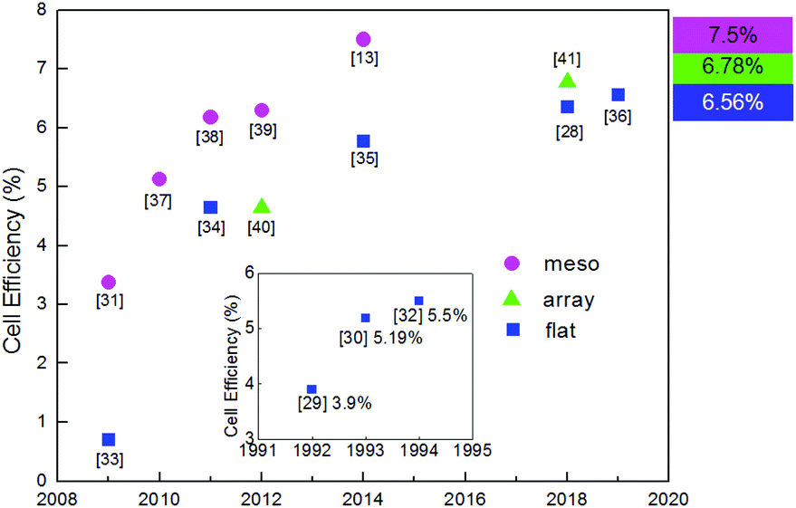 | ||
| Fig. 1 Progress of the PCE of Sb2S3 solar cells. Figures in square brackets indicate reference numbers. The efficiency measurement conditions in the inset are not standard test conditions. | ||
From the aspect of their working mechanisms, Sb2S3 solar cells can be divided into two categories: mesoporous sensitized solar cells and planar heterojunction solar cells. For sensitized Sb2S3 solar cells, which are also sometimes called quantum dot sensitized solar cells, the working mechanism is similar to that of dye sensitized solar cells.42,43 The Sb2S3 nanocrystals deposited on the mesoporous oxide scaffold harvest sunlight first, after which electron–hole pairs are produced in the Sb2S3 layer; then, the electrons are injected into the wide band gap oxide and the holes into the liquid electrolyte or solid hole transporting material (HTM). For planar heterojunction Sb2S3 solar cells, TiO2/Sb2S3/HTM solar cells with similar n–i–p structures have achieved relatively high PCE.13,41 Although their structures are similar to those of high-efficiency n–i–p perovskite solar cells44 and the working mechanism is also assumed to be similar, it is noteworthy that the defect properties and carrier concentrations of lead halide perovskite and Sb2S3 are very different.45,46 In addition, the planar configuration without an HTM layer has delivered attractive PCE recently,47,48 indicating that further investigation of the working mechanism is needed.
Compared with other types of solar cells, Sb2S3 solar cells are less efficient, and much progress is still necessary before they can be used in industry. Limited review articles focusing on Sb2S3 solar cells have been published, and these reviews usually include articles on metal chalcogenide semiconductor planar heterojunctions and sensitized solar cells.42,43,49–51 Wang et al.8 published a review of Sb2(S,Se)3-based solar cells; they presented the synthetic approaches towards Sb2(S,Se)3 films, including Sb2S3 film, for solar cell construction. Kondrotas et al.45 presented a comprehensive review of Sb2S3 solar cells, examined their potential as the front subcell for Si-based tandem solar cells, and provided a roadmap for further technology development. In this review, we focus on the preparation and development of Sb2S3 solar cell functional layers, including their preparation methdologies, morphological structures, optoelectronic properties and corresponding solar cell performance for both planar heterojunction solar cells and mesoporous sensitized solar cells. Sb2S3 films prepared by chemical bath deposition (CBD), spin-coating, vacuum deposition, etc. are first reviewed. Then, the influences of the electron and hole transport materials are examined. Finally, we present some viewpoints toward further PCE improvement from the aspects of material fabrication and device mechanisms.
2. Sb2S3 film fabrication, properties and solar cell efficiency
Most Sb2S3 solar cells reported to date have been deposited by CBD,13,29–33,38,39 spin coating27,28,52–55 or thermal evaporation (TE).56–59 While there have been a few reports of Sb2S3 solar cells produced using atomic-layer deposition (ALD),35,60,61 the in situ hydrothermal approach,62 spray pyrolysis,63 sputtering64,65 and vacuum coating,66 novel synthetic methods to produce uniform, dense Sb2S3 films with fewer defects are still under investigation.Solution processes, including CBD and spin coating, are promising preparation technologies due to their low demand of equipment, simple operation and low cost.67 The CBD method holds two key advantages, one is that film doping can be easily achieved by adding different concentrations of dopants to the chemical bath, and the other is that during the synthesis process, the solution can readily permeate into the porous structure, where the film can co-deposit.45 However, the formation of Sb2O3, SbOCl or other side products cannot be avoided in the conventional aqueous phase CBD technique; this can lead to deep traps and recombination of generated charge carriers.35 The conventional CBD technique usually does not afford large-grained compact films;45 however, the PCE of Sb2S3 solar cells prepared by spin coating is still lower than the best record (7.5%) that was obtained via the CBD method, although the spin-coating-based Sb2S3 film had a large grain size.27 Vacuum deposition can achieve compact, high purity and larger-grained films.45 However, vacuum deposition methods, including TE, ALD and sputtering, have several drawbacks. In the TE process, if a carbon-containing solvent is used, the annealing process is likely to result in carbon residue in the film. The residual carbon can induce recombination sites in the film. The ALD-based film growth rate is low.8
2.1 CBD
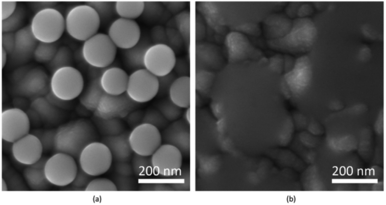
CBD is one of the simplest methods to deposit films of metal sulfides, selenides, oxides, etc.; it has a very long history and has been comprehensively reviewed.68,69 Sb2S3 thin films were deposited by CBD from both acidic and alkaline media in the first report,70 using Sb2O3-EDTA complex and Na2S2O3 as the Sb and S source, respectively. The resulting Sb2S3 films showed optical band gaps of 1.82 to 1.97 eV due to their amorphous states without annealing. Savadogo and Mandal71 later reported a different chemical deposition method involving an aqueous solution of potassium antimonyl tartrate as the Sb3+ source, thioacetamide as the source of S2−, triethanolamine, ammonia, and silicotungstic acid (STA) as a complexing agent. The as-deposited films were amorphous, and annealing at 300 °C for 1 h in a N2 atmosphere led to polycrystalline n type films. From the scanning electron microscopy (SEM) images (Fig. 2), the 300 °C annealed film showed substantial granular growth. The observed binding energy peak of the Sb (3d) energy level in X-ray photoelectron spectroscopy (XPS) for the annealed films demonstrated the impurity of a thin layer of Sb2O3. Various solar cells were prepared using Sb2S3 films in subsequent research; n-Sb2S3/0.01 M KI/C photoeletrochemical solar cells with a PCE of 3.9% at 40 mW cm−2,29 n-Sb2S3/p-Si30 and n-Sb2S3/p-Ge72 heterojunction solar cells with PCEs of 5.19% and 7.3% under AM 1 illumination, and Pt/n-Sb2S3 Schottky barrier solar cells with a PCE of 5.5% under AM 1 illumination31 were obtained.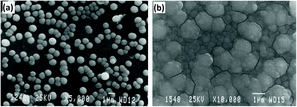 | ||
| Fig. 2 (a) and (b) Sb2S3 film deposited on glass and annealed at 300 °C in a N2 atmosphere for 1 h before and after STA treatment. Reprinted from Savadogo et al.,71 with permission. | ||
To avoid the tendency of hydrolysis when using aqueous media in the CBD method, Messina et al.73 dissolved 650 mg SbCl3 (Aldrich) in 2.5 ml acetone instead of water solution and added 25 ml 1 M Na2S2O3 solution and sufficient water to deposit Sb2S3 thin films. Smooth, specularly reflective thin films were obtained at deposition temperatures from −3 °C to 10 °C. However, the fabricated solar cells with the structure FTO/CdS/Sb2S3/Ag(paint) showed a low current density of 0.02 mA cm−2.
By optimizing the processing conditions of CBD, such as deposition time and pre- and post-treatments, Zimmermann et al.74 fabricated planar heterojunction ITO/TiO2/Sb2S3/hole transport material(HTM)/Ag solar cells with a PCE exceeding 4%. They noted that fine-tuning of the deposition and post-deposition processes was extremely important for achieving high PCEs above 3%. The best device performance was found for compact Sb2S3 layer thicknesses of about 50 to 70 nm with larger crystallites. Although the authors placed the samples tilted face down into the bath to avoid large particles, large crystallites ∼1 μm in size were widely distributed on the film surface, as shown in the SEM image (Fig. 3).
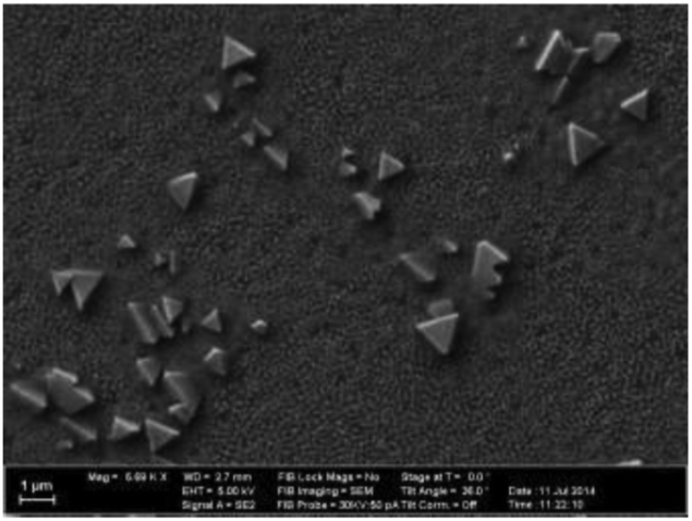 | ||
| Fig. 3 Scanning electron microscopy image of the Sb2S3 surface. Reprinted from Zimmermann et al.,74 with permission. | ||
Sb2S3 was deposited on nanoporous TiO2 (Degussa, P25) film by CBD for the first time in 2009 by Itzhaik et al.31 The as-deposited Sb2S3 layer thickness was estimated to be in the range of 5 to 10 nm from SEM images. The authors stated that X-ray diffraction (XRD) showed the presence of some Sb2O3 when Sb2S3 was removed hot from the oven and allowed to cool in air. Due to the fact that much poorer performance was obtained if the as-deposited Sb2S3 film was cooled under N2, the authors assumed that the surface oxide Sb2O3 acted as a passivation layer. The conversion efficiency reached 3.37% for the FTO/c-TiO2/mp-TiO2/In-OH-S/Sb2S3/KSCN/CuSCN/Au cell structure.
With increasing deposition time, the thickness of Sb2S3 layers deposited onto mesoporous TiO2 films should increase, which is expected to have a remarkable effect on the solar cell performance. Chang et al.37 investigated the effects of Sb2S3 CBD times from 1 to 4 h in FTO/TiO2/Sb2S3/P3HT-sensitized solar cells. The deposited Sb2S3 showed a broad distribution of particle sizes or thin layers. Large particles were also observed in the cross-section SEM image of the device, probably due to Sb2S3 (Fig. 4a). The absorbance of the Sb2S3-sensitized films increased with the Sb2S3 deposition time (t) from 1 to 4 h (Fig. 4b). Meanwhile, a thicker Sb2S3 layer (t = 4 h) exhibited decreased values of incident-photon-to-current efficiency (IPCE), current density (Jsc) and Voc compared to the Sb2S3 layer obtained at t = 3 h (Fig. 4c). The thick absorber layers may increase the charge carrier recombination before they are injected into the electron and hole conductors.75 A device under the deposition time of 3 h demonstrated 5.06% and 5.13% PCE before and after adding the interfacial modifier decylphosphonic acid (DPA).
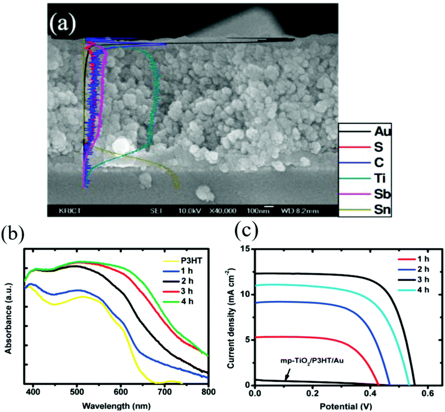 | ||
| Fig. 4 (a) Cross-section SEM image of FTO/TiO2/Sb2S3/P3HT. (b) Absorption spectra of P3HT and Sb2S3-deposited mp-TiO2 for various deposition times on the surface of mesoporous TiO2 layers in a chemical bath. (c) Current density–voltage (J–V) curves for TiO2/P3HT/Au and TiO2/Sb2S3/P3HT/Au fabricated with different deposition times. Reprinted from Chang et al.,37 with permission. | ||
Gui et al.76 also investigated the influence of CBD time on solid Sb2S3 sensitized solar cells. They evaluated the grain sizes of the Sb2S3 samples from their XRD patterns using Scherrer's equation; there were no significant differences in the films deposited for 1 h, 2 h, or 3 h, all of which contain grains about 19 to 20 nm in size. It is noteworthy that there is usually inaccuracy when employing Scherrer's equation, especially due to the fact that deposited Sb2S3 has a broad distribution of particle sizes. In addition, diffraction peaks corresponding to Sb2O3 phase with orientations of (111) and (222) were observed in the XRD patterns (Fig. 5a). After the chemical bath deposition, a surface treatment consisting of thermal oxidation and subsequent HCl etching of the Sb2S3 layer was introduced to improve the solar cell performance (Fig. 5b). The best PCE of 2.32% was obtained for the 3 h CBD time, and the optimal particle size of the TiO2 mesoporous film (∼2 μm) was 100 nm.
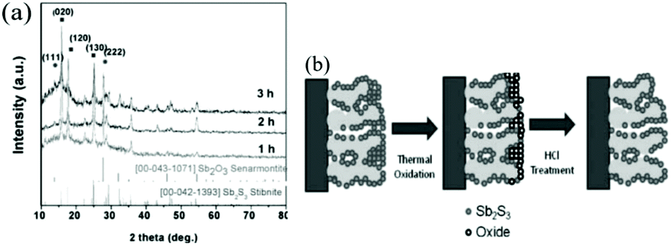 | ||
| Fig. 5 (a) X-Ray diffraction patterns of 1 h, 2 h and 3 h-deposited Sb2S3 films. (b) Schematic of a surface modification consisting of a 2-step treatment: (i) thermal oxidation, (ii) HCl treatment. Reprinted from Gui et al.,76 with permission. | ||
Thioacetamide (TA) was used to sulfurize the surface of Sb2S3, decreasing the content of oxide impurities and improving the performance of solid Sb2S3-sensitized solar cells, by Choi et al.13 The 0.01 g mL−1 TA solutions diluted in DMF were spin coated on DMF-treated FTO/BL-TiO2/mp-TiO2/Sb2S3 at 3000 rpm for 60 s; then, the samples were annealed at 300 °C. Hydrogen sulfide (H2S) decomposed from TA reacted with the surface Sb2O3 to form Sb2S3, and the assumed reactions are:
| CH3CSNH2 → CH3CN(g) + H2S(g) |
| Sb2O3 + 3H2S(g) → Sb2S3 + 3H2O(g) |
TA treatment decreased the amount of Sb2O3, as confirmed by the XPS spectra (Fig. 6a and b); the relative atomic ratio of Sb2O3/Sb2S3 dramatically decreased from 49/51 to 20/80 after TA treatment. The untreated Sb2S3 film showed hole traps (Ev + 0.52 eV) with a defect density of about 2 to 5 × 1014 cm−3. The average PCE of the TA-treated devices (∼5.5%) was about 0.8% higher than that of the untreated devices (∼4.7%). To improve the performance of Sb2S3-sensitized solar cells obtained by TA treatment, they studied the Sb2S3 CBD reaction time. The most efficient devices were obtained after 2 h 20 to 25 min. The best device exhibited a PCE of 7.5%, which is the highest reported for Sb2S3-based solar cells to date (Fig. 6c).
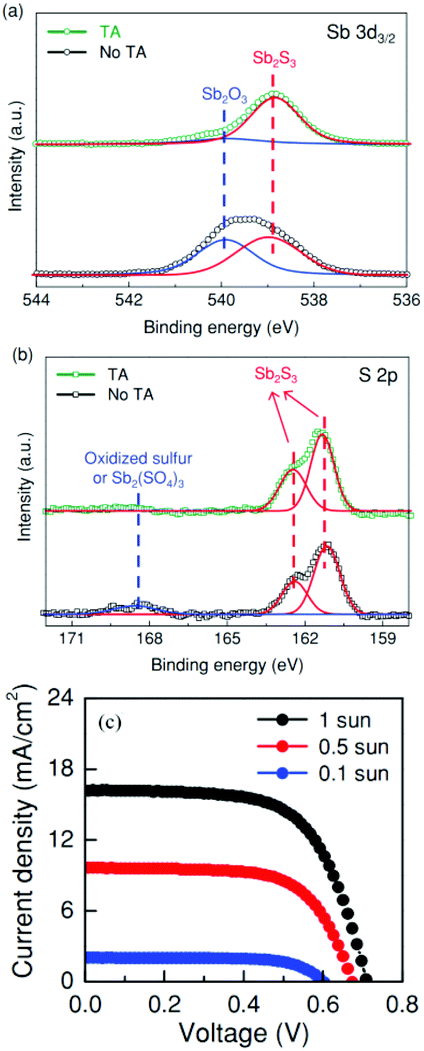 | ||
| Fig. 6 Effects of TA sulfurization on the surface states of Sb2S3. High resolution XPS spectra of (a) Sb3d3/2 and (b) S2p of samples with TA and without TA. (c) J–V characteristics of the best cell. Reprinted from Choi et al.,13 with permission. | ||
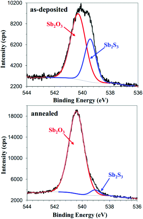
As mentioned above, oxide impurities are sometimes considered to act as a passivation layer and have beneficial effects on Sb2S3 solar cells.31,77,78 Gödel et al.77 investigated the effects of post heat treatment of CBD-deposited Sb2S3 samples on solid Sb2S3-sensitized solar cells in air for different times from 0 to 20 min. UV-vis measurements did not show obvious changes; also, the peaks of antimony oxide did not appear in the XRD spectra. The author pointed out that absorption spectroscopy measures the bulk properties of a material sensitively instead of the thin surface layers. Also, antimony oxide did not exist as crystals. XPS measurements of the films showed a Sb3d3/2 peak at 539.5 eV corresponding to antimony oxide (SbxOy); the intensity of the peak increased with increasing annealing time. From the J–V curves of the samples, short annealing times were beneficial to the PCE; the best PCE of 2.4% was obtained after annealing for 1 min at 200 °C in air (Fig. 7). Itzhaik et al.78 estimated the Sb2O3 overlayer thickness in a TiO2/In-OH-S/Sb2S3 film to be 3 to 5 nm or 1 nm according to XPS and energy-dispersive X-ray spectroscopy (EDS), respectively, for the standard air-cooled Sb2S3 film after CBD and N2 annealing. A grain radius of Sb2S3 of 10 nm was used for the EDS thickness evaluation, while the authors noted that in reality, Sb2S3 grains appeared in clusters with radii ca. 40 nm; some even had radii of 100 nm. They further pointed that the Sb2O3 thin layer effectively presented a ca. 1 eV barrier to hole transport according to the raw XPS valence band spectra of the Sb2S3 film (Fig. 8).
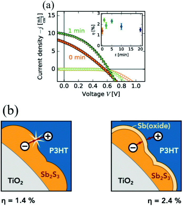 | ||
| Fig. 7 (a) J–V characteristics of an unannealed and an annealed (1 min) solar cell under 1 Sun illumination (full symbols) and in the dark (open symbols). The inset shows the averaged efficiencies for different annealing times in air. (b) Surface oxidation by controlled heat treatment in air leads to improved Sb2S3-sensitized solar cells by decreasing the charge carrier recombination. Reprinted from Gödel et al.,77 with permission. | ||
 | ||
| Fig. 8 Sb3d3/2 XPS spectra of the as-deposited (top) and annealed (bottom) Sb2S3 film on TiO2/In-OH-S substrate. The Sb signal is composed of both Sb2S3 and Sb2O3 components. Reprinted from Itzhaik et al.,78 with permission. | ||
The reactions of conventional CBD must be slowed by cooling below 10 °C to avoid immediate precipitation.79 This is disadvantageous for large-scale applications at low temperatures. Gödel et al.80 presented a room temperature deposition route of Sb2S3 using the same precursor materials (SbCl3 and Na2S2O3) as the conventional CBD method. They changed the order of reactant addition at room temperature to slow the formation of Sb2S3 on 1 μm thick TiO2 mesoporous films composed of 50 nm particles. The average Sb2S3 crystallite sizes were calculated to be 40 nm and 35 nm for room temperature and conventional low temperature deposition, respectively, from the XRD patterns (Fig. 9a). These values are relatively large compared with the average particle and pore sizes of the mesoporous TiO2 film (∼50 nm). The RT sample had a marginally higher oxide content compared to the low-T material by XPS measurements (Fig. 9b). There was a clear decrease in the density of deep-trap states for the RT-deposited Sb2S3 based on photo-thermal deflection spectroscopy (PDS) (Fig. 9c). The best device of the FTO/c-TiO2/mp-TiO2/Sb2S3/PCPDTBT:PCBM/PEDOT:PSS/Au structure achieved a PCE of 5.1% using the room temperature deposition method.
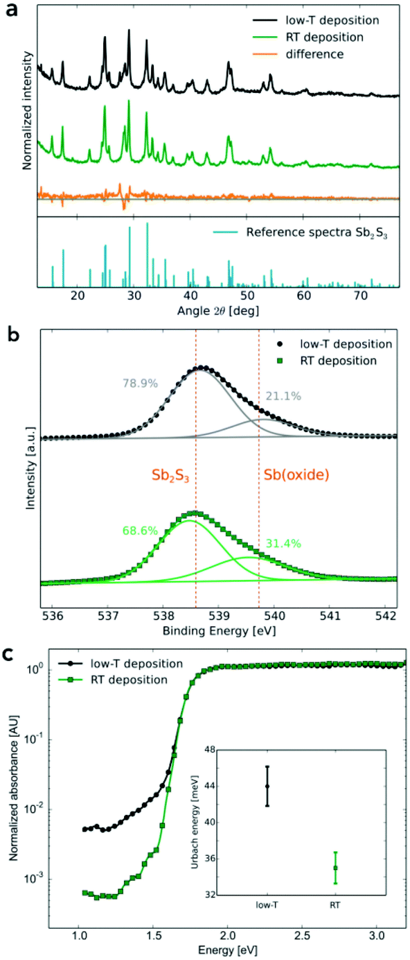 | ||
| Fig. 9 (a) XRD pattern of crystalline Sb2S3, synthesised via the low temperature deposition method (upper trace) and the RT technique (center trace). The lower trace shows the difference of the two patterns. The stibnite reference pattern was taken from ref. 15. (b) XPS Sb3d3/2 peaks of the films obtained from both deposition methods. The solid lines show the least squares fit of a superposition of two Gaussian curves. (c) PDS measurements showing the sub-band-gap energy levels for both deposition methods. The inset shows the corresponding Urbach energies. Reprinted from Gödel et al.,80 with permission. | ||
2.2 Spin-coating
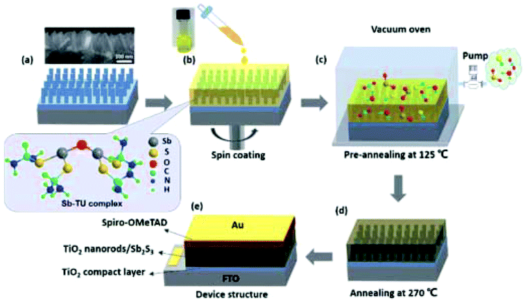
The conventional CBD method requires a relatively long deposition time, and control of the size or the thickness of the Sb2S3 layer is difficult. The formation of impurities, including SbOCl and antimony oxides, cannot be avoided thoroughly, resulting in deep traps and causing backward recombination of the generated charge carriers. The spin-coating method has the advantages of fast processes and has been extensively investigated in organic and inorganic thin film preparation.81–83 Especially, this method has earned great success in the fabrication of lead halide perovskite optoelectronic devices44,84–86 and shows enormous room for further improvement.Choi et al.52 first spin coated a SbCl3-thiourea (Sb-TU) complex solution on a mesoporous TiO2 film to fabricate efficient Sb2S3-sensitized solar cells. The Sb2S3 loading amounts were simply controlled by tuning the mole concentrations of SbCl3 and thiourea in solution, enabling them to obtain an exact ratio of S/Sb in the final product (Fig. 10a). The EDX line scan profile showed the uniform distribution of Sb and S elements along the mesoporous TiO2 layer, as observed in Fig. 10b and c, confirming the uniform deposition of Sb2S3 inside the pores of the mp-TiO2 layer. The most efficient device was obtained under specific conditions of the ratio of SbCl3![[thin space (1/6-em)]](https://www.rsc.org/images/entities/char_2009.gif) :TU = 1:1.8. The best device exhibited a high device efficiency of 6.4%.
:TU = 1:1.8. The best device exhibited a high device efficiency of 6.4%.
 | ||
| Fig. 10 (a) Schematic of the fabrication process of our devices via Sb-TU complex solution processing. (b) Cross-sectional FESEM image of a typical device and (c) EDX line scan profile along the L1 layer. For the EDX line scan profile analysis, the sample was deposited on glass (not FTO) to avoid misinterpretation between two elements, i.e., Sb of Sb2S3 and Sn of FTO. Reprinted from Choi et al.,52 with permission. | ||
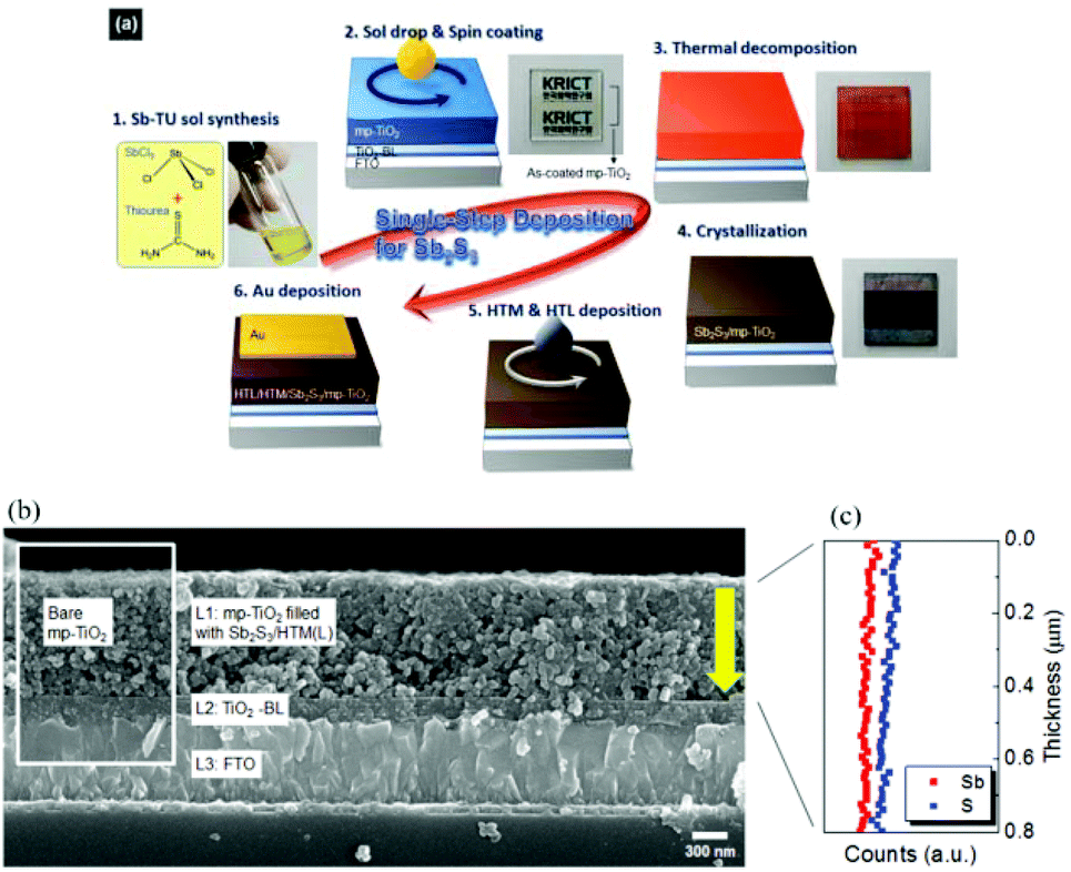
A vacuum annealing process just after the spin-coating process was employed to fabricate highly efficient solar cells.41 SbCl3 and thiourea source materials were dissolved in 2-methoxyethanol. The solution precursors were spin coated onto TiO2 nanorod arrays in order to fabricate a Sb2S3-sensitized device architecture. The optimized pre-annealing temperature was 125 °C for the vacuum-assisted solution process (VASP) approach. Finally, the film was annealed at 270 °C under a N2 atmosphere to improve the crystallinity (Fig. 11). The highest PCE of the FTO/bl-TiO2/TiO2 nanorods array/Sb2S3/Spiro-OMeTAD/Au device reached 6.78%.
 | ||
| Fig. 11 Schematic of the fabrication process of Sb2S3-based devices via vacuum-assisted solution processing. Reprinted from Tang et al.,41 with permission. | ||
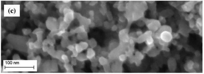
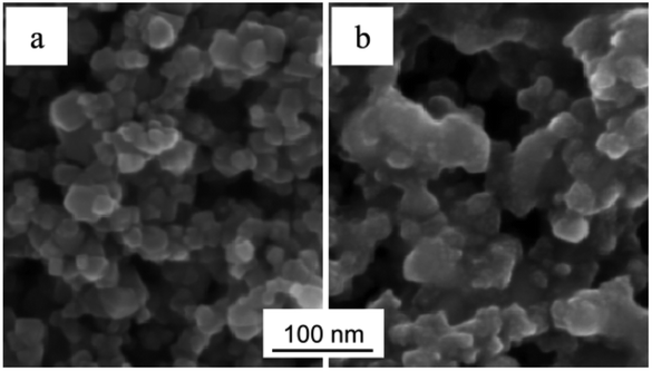
The modified spin-coating method using 2-methoxyethanol as the precursor solvent was also applied in planar solar cells with the structure of FTO/c-TiO2/Zn–Sb2S3/Spiro-OMeTAD/Au.28 In addition, ZnCl2 was introduced into the precursor solution to dope Sb2S3 films. The Zn doping considerably increased the number of sulfur vacancies, which in turn increased the electron concentration in the final Sb2S3 film. In addition, the doping of Zn ions regulated the film growth and enhanced the crystallinity. However, a much higher doping concentration caused an increase of pinholes in the film (Fig. 12). The final PCE of the Sb2S3 planar solar cells reached 6.35%.
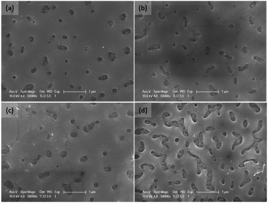 | ||
| Fig. 12 SEM images of the Sb2S3 film by spin-coating: as-synthesized pristine (a) and with Zn doping of 1.5% (b), 4.8% (c), and 8.6% (d). Reprinted from Tang et al.,28 with permission. | ||
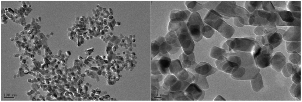
In addition to the precursor materials of SbCl3 and thiourea, Wang et al.27 developed a novel precursor for spin-coating Sb2S3 films. They used Sb2O3 as a Sb-source that was dissolved in carbon disulphide (CS2) and n-butylamine mixed solution, forming an antimony-complex precursor solution. By spin-coating the precursor solution on a substrate and annealing at 300 °C for only 2 min, Sb2S3 film with a lateral grain size of up to 12 μm could be obtained; the average size was about 6 μm and the thickness of the Sb2S3 film was ∼137 nm (Fig. 13a and b). A large grain size was favorable for charge transport across the film, and the resulting planar FTO/bl-TiO2/Sb2S3/Spiro-OMeTAD/Au solar cell delivered a PCE of 4.3%. Subsequently, the same group used the spin-coating approach to deposit Sb2S3 films; V2O555 and NiOx87 acted as HTMs. The PCE of devices based on Sb2S3/V2O5 and Sb2S3/NiOx reached 4.8% and 3.51%, respectively. Recently, they modified the method by applying ethanol and dimethyl sulfoxide as dissolution solvents to increase the boiling point of the mixed solvent and introduced alkali hydroxides (LiOH, NaOH, KOH, RbOH, CsOH)36 into the precursor solution to dope Sb2S3 films. It was found that K, Rb and Cs were beneficial to large Sb2S3 grain growth and better morphology (Fig. 13c) along with an upshift of the Fermi energy level, which facilitated the charge transport from Sb2S3 to TiO2. The Cs-doped planar FTO/c-TiO2/Cs–Sb2S3/Spiro-OMeTAD/Au solar cell delivered the best PCE of 6.56%, which is the record efficiency for planar Sb2S3 solar cells.
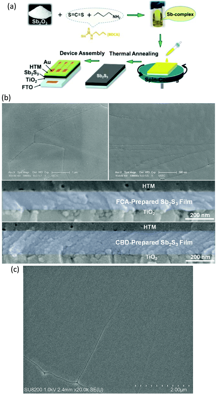 | ||
| Fig. 13 (a) Schematic of the synthesis of the Sb2S3 film and device assembly. (b) SEM images of the Sb-complex films annealed at different temperatures and cross sectional SEM images of the devices containing FCA and CBD-fabricated Sb2S3 films. (c) SEM image of the Cs-doped Sb2S3 film. Reprinted from Wang et al.,27,36 with permission. | ||
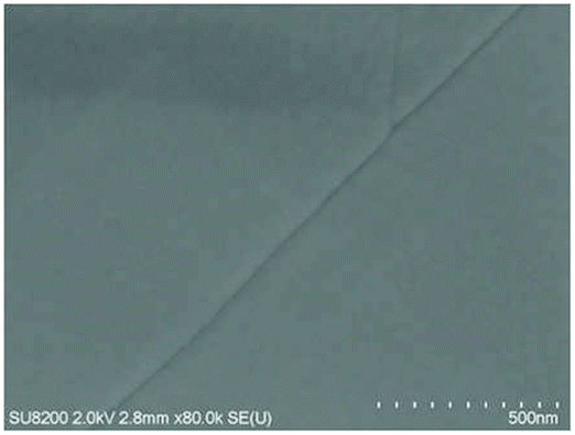
The same group88 reported an aqueous precursor solution composed of Sb2O3, 3-mercaptopropionic acid and aqueous ammonia. 3-Mercaptopropionic acid acted as both the solvent and sulfur source, while aqueous ammonia facilitated the formation of a homogenous thiol-containing Sb-complex solution. Thermal decomposition at 270 °C after spin-coating produced compact, flat, uniform and well-crystallized Sb2S3 films (Fig. 14). A planar Sb2S3 solar cell with the structure of FTO/bl-TiO2/Sb2S3/Spiro-OMeTAD/Au delivered a PCE of 5.57%.
 | ||
| Fig. 14 SEM image of a Sb2S3 film prepared with an annealing temperature of 270 °C; cross section of the fabricated Sb2S3 solar cell. Reprinted from Li et al.,88 with permission. | ||
A convenient two-step sequential spin-coating approach was suggested by Zhang et al.89 Antimony acetate (Sb(Ac)3) solution using DMSO as a solvent was first spin-coated; then, thiourea solution, also using DMSO as the solvent, was spin-coated. Annealing at 320 °C caused Sb(Ac)3 and thiourea to react to form a Sb2S3 film very quickly, in less than 2 min (Fig. 15). By optimizing the thiourea solution concentration, a planar FTO/bl-TiO2/Sb2S3/Spiro-OMeTAD/Au device delivered a PCE of 5.69%.
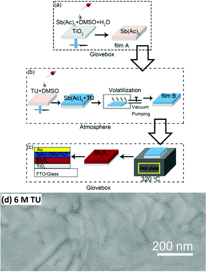 | ||
| Fig. 15 Schematic of the film deposition and device fabrication. (a) Spin-coating Sb(Ac)3 in DMSO solution for the fabrication of the Sb(Ac)3 film (film A). (b) Deposition of thiourea (TU) on the surface of film A, followed by dissociating the organic molecules using a vacuum pump (film B). (c) Annealing of film B at an elevated temperature for the formation of the crystallized Sb2S3 film and device assembly. (d) High magnification surface SEM images of the Sb(Ac)3 film reacted with spin-coated TU with concentrations of 6 M TU, followed by annealing at 320 °C for 2 min. Reprinted from Zhang et al.,89 with permission. | ||
Zheng et al.90 developed a sequential solid–gas deposition method to prepare solid Sb2S3 sensitized solar cells, first spin-coating SbCl3 aqueous solution followed by reaction with H2S gas and further annealing (Fig. 16a). The loading amount of Sb2S3 within the porous TiO2 film could be easily controlled through adjusting the concentration of SbCl3 solution. From the SEM results, Sb2S3 was homogeneously coated within the mesoporous TiO2 film, which was attributed to the in situ solid–gas reaction between SbCl3 pre-coated on the TiO2 film and H2S, in contrast to the heterogeneous nucleation and growth process in the CBD process. Moreover, the method afforded pure Sb2S3 and no Sb2O3 on the surface based on XPS (Fig. 16b). A PCE of 6.27% was achieved for the optimized Sb2S3 sensitized solar cells.
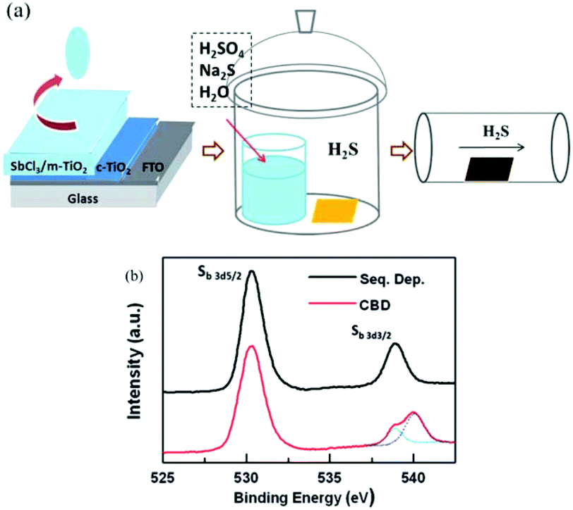 | ||
| Fig. 16 (a) Schematic of the deposition of a Sb2S3 layer on the TiO2/FTO substrate by the sequential deposition process. (b) XPS Sb3d spectra of Sb2S3 obtained from sequential deposition (with a SbCl3 concentration of 16 mg ml−1) and CBD. Reprinted from Zheng et al.,90 with permission. | ||
Spin-coating of pre-synthesized nanomaterials has been extensively investigated in the field of quantum dot optoelectronics.91,92 Wang et al.93 reported the synthesis of colloidal Sb2S3 nanoparticles by a hot-injection method; they applied the pre-synthesized Sb2S3 nanoparticles in planar solar cells by spin-coating on TiO2-covered FTO substrates. Solar cells based on these nanoparticles achieve a PCE of 1.5%, which is the record efficiency for planar hybrid solar cells based on Sb2S3 nanoparticles. It is clear from the SEM images that there is much room to achieve uniform and dense Sb2S3 nanoparticle films (Fig. 17).
 | ||
| Fig. 17 SEM images of Sb2S3 NPs on TiO2-covered FTO substrates (a) before and (b) after annealing. Reprinted from Wang et al.,93 with permission. | ||
2.3 Vacuum deposition
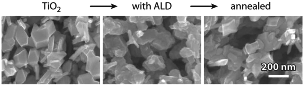
During the early stages, when Sb2S3 found applications in television cameras, microwave devices, etc., Sb2S3 films were prepared by the vacuum evaporation technique.94–96 Compared with the Sb2S3 films obtained from solution processes such as CBD and spin-coating, the Sb2S3 films deposited by vacuum routes were formed with smooth and compact surface morphologies, free of impurities such as antimony oxides. However, TE,34,58–60,66,97 sputtering (SP)64,65 and ALD35,60,61,98 based on vacuum technology have been used to prepare Sb2S3 solar cells only recently.ALD essentially combines the advantages of fine thickness control and high purity. Wedemeyer et al.60 first employed the method to prepare solid Sb2S3-sensitized solar cells. With accurate growth rate control, the thickness of the Sb2S3 layer was tuned from 3 to 13 nm. The disappearance of the initially visible sharp edges of the TiO2 crystals demonstrated the conformal coating (Fig. 18). A PCE of 2.6% was achieved for the 10 nm Sb2S3-sensitized solar cells. Kim et al.35 later employed ALD to fabricate planar FTO/bl-TiO2/Sb2S3/P3HT/PEDOT:PSS/Au solar cells; the optimal thickness of the Sb2S3 layer was 90 nm. There was significant improvement from the aspects of Sb2S3 thickness control, deposition reproduciblity and purity against oxides based on the tranmission electron microscopy (TEM), spectroscopic ellipsometry and XPS measurements (Fig. 19a and b). The optimized device delivered a PCE of 5.77%.
 | ||
| Fig. 18 Microstructures of mesoporous solar cells based on Sb2S3 obtained by ALD. Changes observed by SEM (top view) upon ALD and annealing. Reprinted from Wdemeyer et al.,60 with permission. | ||
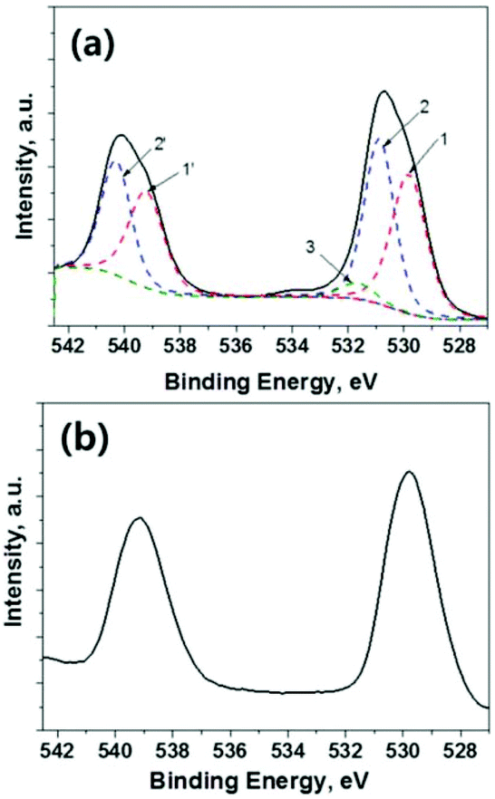 | ||
| Fig. 19 XPS Sb3d spectra of Sb2S3 obtained from the (a) conventional CBD process and (b) ALD process. The solid line is the experimental data and the dotted line is the fitted data. 1 (Sb2S3) = Sb3d5/2, 1′ (Sb2S3) = Sb3d3/2, 2 (Sb2O3) = Sb3d5/2, 2′ (Sb2O3) = Sb3d3/2, 3 = O1s. Reprinted from Kim et al.,35 with permission. | ||
Thermal evaporation is a conventional cost-effective vacuum deposition method that has been successfully used to fabricate various planar Sb2S3 solar cells.47,58,59,66,97,99–101 Recently, Yin et al. reported the composition engineering of Sb2S3 film by co-evaporation of sulfur or antimony with Sb2S3 (Fig. 20). By controlling the ratios between Sb2S3 and S or Sb during thermal evaporation, the sulfur-rich Sb2S3 film-based device showed high carrier concentration and decreased recombination probability compared with the pristine and antimony-rich Sb2S3-based devices. With the thermally evaporated Sb2S3 thin films, the best PCE was 5.8% for the glass/FTO/bl-TiO2/TiO2 array/Sb2S3/Spiro-OMeTAD/Au planar devices.102 In addition, post-treatment in Se atmosphere was combined with rapid thermal evaporation to improve junction quality, passivate absorber defects, decrease the back contact barrier and therefore enhance the solar cell PCE.47,101
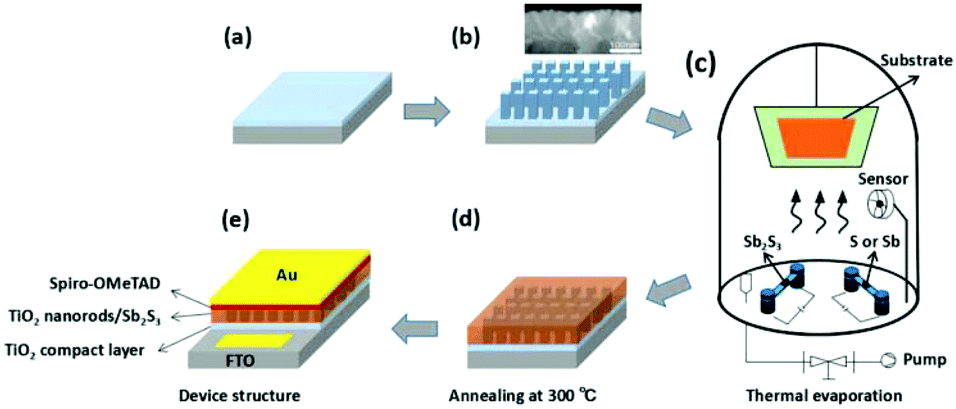 | ||
| Fig. 20 Schematic of the fabrication process of the Sb2S3-based device via thermal evaporation. Reprinted from Yin et al.,102 with permission. | ||
Deng et al.48 proposed a facile strategy to achieve quasiepitaxy growth of Sb2S3 film on TiO2 surfaces for the first time. Engineering the TiO2 exposure facets through the annealing temperature induced quasiepitaxial growth of vertical orientation Sb2S3 films by rapid thermal evaporation. The authors systematically investigated the epitaxial effect by morphology, lattice structure and physical characterization. The interface defects and Sb2S3 absorber transport loss were overcome, and the optimal device delivered a PCE of 5.4%, which is the best reported for full-inorganic Sb2S3 solar cells.
3. Electron transporting materials (ETM)
Sb2S3 solar cells usually employ a sandwiched structure of ETM/Sb2S3/HTM. These devices need the assistance of ETM and HTM to extract the carriers. By choosing different electron conductors, such as SnO2,29,62,103 CdS,33,47,58,73,99,104 ZnO,56,57,61,63 and TiO2,13,31,37,38,105–108 much progress has been achieved in Sb2S3 solar cells.SnO2 is a wide band-gap metal oxide semiconductor (∼3.8 eV);109 the carrier mobilities of single crystal SnO2 and nanostructured SnO2 are ∼250 cm2 V−1 s−1 (ref. 110) and ∼125 cm2 V−1 s−1,111 respectively. Early in 1992, Savadogo and Mandal fabricated Sb2S3 solar cells with a glass/SnO2/Sb2S3/graphite structure. The efficiency reached 3.9% under 40 mW cm−2 illumination.29 Subsequently, SnO2 has rarely been used as an ETM. Lei et al.103 employed ∼40 nm thick SnO2 film as an ETM to fabricate FTO/SnO2(∼40 nm)/Sb2S3/P3HT/Au devices in 2016. The best-performing solar cells reached a PCE of 2.8%.
ZnO has a high electron mobility (μe = ∼200 cm2 V−1 s−1) and a wide band gap (Eg = ∼3.2 eV).112 However, the PCE of the Sb2S3 solar cells with ZnO as the ETM was relatively low. Liu et al.57 prepared polycrystalline thin films of ZnO with a thickness of ∼60 nm by spin casting followed by thermal annealing in air at 350 °C for 20 min. The best PCE of the ITO/ZnO(n)(∼60 nm)/Sb2S3(i)(50 to 350 nm)/P3HT(p)/Ag structure device was 2.4%. Jo et al.61 prepared a∼ 30 nm thick ZnO layer using the ALD method. They indicated that the ALD-processed ZnO had good crystal quality. The device structure was FTO/ZnO/Sb2S3/P3HT/Au, and an efficiency of 2.81% was delivered. Although the electron mobility of the ZnO layer is high, the hole mobility of P3HT is low (10−5 to 10−3 cm2 V−1 s−1),113 which hinders the efficiency enhancement.
Most commonly, a mesoporous TiO2 layer (mp-TiO2)13,31,37–39,76–78,80,105,114–117 or compact TiO2 (c-TiO2) layer28,53–55,59,87,97,100,101 is used as the ETM for Sb2S3 solar cells. In the first attempt to fabricate Sb2S3-sensitized solar cells by Itzhaik et al.,31 they designed the structure of FTO/c-TiO2/mp-TiO2/In-OH-S/Sb2S3/KSCN/CuSCN/Au using a nanoporousTiO2 film (1 to 2 μm thick, 25 nm particles) as the ETM. The deposition often covered several TiO2 particles, as shown in Fig. 21. Subsequently, Moon et al.114 also deposited Sb2S3 onto the nanoporous TiO2 substrate. The thickness and particle size of the nanoporous TiO2 film were ∼2 μm and 30 nm, respectively. The Sb2S3 did not cover each TiO2 particle conformally but rather coated clusters of TiO2 (Fig. 22). A TiO2 film composed of 20 nm-sized nanoparticles had a smaller pore size than films comprising 30 nm particles; the device made of 20 nm TiO2 nanoparticles yielded an efficiency of less than 1%. The particle size of the nanoporous TiO2 film was increased to 60 nm by Chang et al.;37 the cells of the FTO/dense-TiO2/mp-TiO2/Sb2S3/P3HT/PEDOT:PSS/Au structure reached 5.13% PCE (Fig. 23).
 | ||
| Fig. 21 SEM images of an Sb2S3 film on P25/In-OH-S substrate. Reprinted from Itzhaik et al.,31 with permission. | ||
 | ||
| Fig. 22 SEM pictures of (a) bare 30 nm TiO2 particles and (b) the Sb2S3 film deposited and annealed on a 30 nm TiO2/In-OH-S substrate. Reprinted from Moon et al.,114 with permission. | ||
 | ||
| Fig. 23 TEM photographs of TiO2 nanoparticles. Reprinted from Chang et al.,37 with permission. | ||
Gui et al.76 fabricated devices of FTO/c-TiO2/mp-TiO2/In-OH-S/Sb2S3/P3HT/PEDOT:PSS/Au with larger TiO2 nanoparticles (∼50 nm and ∼100 nm) for comparison. The porosities and surface areas of the TiO2 films were characterized with BET. The surface area and pore size of the film consisting of 50 nm TiO2 nanoparticles were 128.31 m2 g−1 and 52 nm, respectively. The film consisting of ∼100 nm nanoparticles showed a surface area of 13.36 m2 g−1 and a pore size of 120 nm. For larger-size nanoparticle films, a larger porosity probably facilitates access of the precursor into the TiO2 pores.
The thickness of nanoporous–TiO2 films is generally controlled to be about 1 to 3 μm. Boix et al.115 decreased the TiO2 film thickness and studied the effects on the performance of FTO/c-TiO2/mp-TiO2/Sb2S3/P3HT/Au(NS) and FTO/c-TiO2/Sb2S3/P3HT/Au (flat) solar cells by impedance spectroscopy. The NS solar cells presented higher performance than the flat cells due to their higher Jsc and fill factor (FF). Conversely, Voc was higher for the flat device. The impedance spectroscopy analysis showed that decreasing the effective surface area of the flat cells decreased the recombination rate and increased the open circuit potential, Voc; meanwhile, charge compensation problems as a consequence of inefficient charge screening in the flat cells increased the hole transport resistance, severely decreasing the cell Jsc and fill factor. Muto et al.116 obtained a similar relationship between the cell performance and the TiO2 film thickness. Tsujimoto et al.105 also found variation of the PCE of FTO/c-TiO2/mp-TiO2/Sb2S3/KSCN/CuSCN/Au solar cells related to the TiO2 particle size. The optimized thickness of the nanoporous–TiO2 films was fixed as 2.5 μm. When the particle size was increased to 30 nm, the conversion efficiency increased to 3.65% and then decreased with further increase of the particle size. The larger TiO2 particles led to a smaller surface area, resulting in lower photon absorption and a lower photocurrent density.
The surface treatment of ETM nanoparticles is expected to improve the charge extraction at the TiO2/Sb2S3 interface. Tsujimoto et al.105 treated the mesoporous–TiO2 surface by Mg2+, Ba2+, and Al3+. The short-circuit current density was improved with Mg2+. The FF was improved with Ba2+. The open-circuit voltage was improved with both Al3+ and Ba2+. However, the starting material for Al3+ treatment, AlCl3, was quite unstable, resulting in inconsistent results. Excluding Al3+, therefore, Mg2+ and Ba2+ were chosen for double treatment. The best efficiency obtained using Ba2+/Mg2+ double treatment was 4.1%. Fukumoto et al. treated Sb2S3-sensitized TiO2 films with DPA to decrease recombination. The DPA-treated devices exhibited increased Voc and FF.117 Xu et al.107 utilized ultrathin SiO2 films with thicknesses of 0.6 to 1.6 nm (Fig. 24) as a blocking layer to suppress the interfacial recombination at the TiO2/Sb2S3 interface, which was the major recombination path in the solar cells as confirmed by impedance spectra and open-circuit voltage-decay analysis. The efficient injection of photoinduced electrons from Sb2S3 to TiO2 was not impeded due to the ultrasmall thickness of the SiO2 layer. The SiO2 passivated liquid Sb2S3-sensitized solar cells exhibited increased PCE from 3.00% to 3.96%.
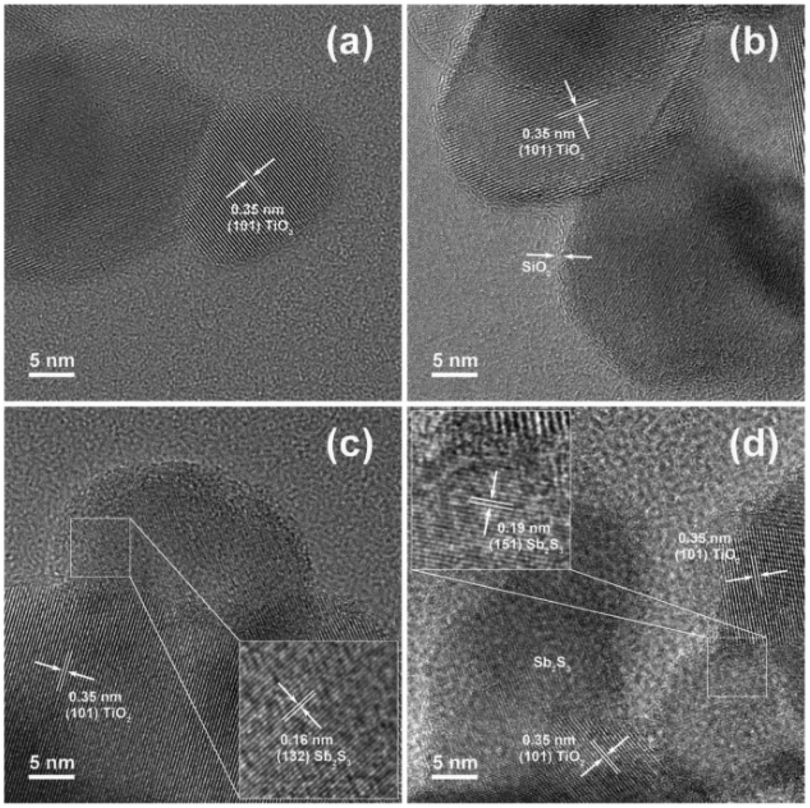 | ||
| Fig. 24 HRTEM images of (a) bare TiO2, (b) TiO2/SiO2, (c) TiO2/crystalline Sb2S3 and (d) TiO2/SiO2/crystalline Sb2S3. Reprinted from Xu et al.,107 with permission. | ||
In addition, the surface morphology structure of TiO2 films has an important effect on the performance of the planar Sb2S3 solar cells. Sung et al.54 reported that a smooth surface morphology of TiO2 layers (BL1) was unfavorable to the formation of uniform and dense high-quality Sb2S3 absorber layers during the spin-coating process (Fig. 25). In contrast, due to the lower surface energy, more compact Sb2S3 films formed on the rough TiO2 layers (BL2). A high-quality Sb2S3 absorber layer could improve the photovoltaic performance of planar Sb2S3 solar cells, with the cell corresponding to a thiourea/Sb ratio of 2.0 showing the best performance of 3.8% PCE.
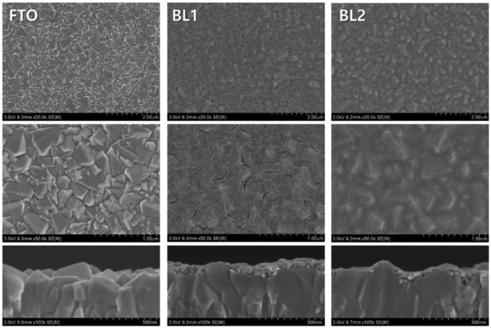 | ||
| Fig. 25 SEM images of FTO, BL1, and BL2 blocking layers. Reprinted from Sung et al.,54 with permission. | ||
To reduce contact between Sb2S3 and the oxide ETMs (TiO2, SnO2 or ZnO), Tang's group fabricated planar Sb2S3 solar cells using CdS as an ETM without a HTM; the cell structure was ITO/CdS/Sb2S3/Au. The thickness of the CdS was about 60 nm. The CdS/Sb2S3 solar cells achieved a PCE of 4.17%, which is the highest efficiency Sb2S3 solar cell using CdS as the ETM at present.
4. Hole transporting materials (HTM)
HTMs are used to extract holes from Sb2S3. Different HTMs, including poly(3-hexylthiophene) (P3HT),35,37,90,107,108,115 2,2′,7,7′-tetrakis-(N,N-di-p-methoxyphenyl-amine)-9,9′-spirobifluorene (spiro-MeOTAD),27,41,66,114,118 poly(2,6-(4,4-bis-(2-ethylhexyl)-4H-cyclopenta[2,1-b;3,4-b′]dithiophene)-alt-4,7(2,1,3-benzo-thiadiazole) (PCPDTBT),39,80 poly(triarylamine) (PTAA), CuSCN,31,78,105 V2O5,55 NiOx87 and graphene,119 have been employed in Sb2S3 solar cells. Enhancing the hole-transporting properties of Sb2S3 solar cells is important for further increasing their efficiency.
As an efficient hole-transporting material, spiro-OMeTAD has been widely applied in solid-state dye-sensitized solar cells and perovskite solar cells.42 Spiro-MeOTAD was first employed as the HTM in solid Sb2S3 sensitized solar cells by Moon et al.;114 it was coated on the TiO2/Sb2S3 film by spin coating. Due to the fact that the conductivity of spiro-OMeTAD is significantly improved with suitable p-type dopants,120 Chung et al.118 employed DPA as an effective p-doping additive in the presence of lithium bis(trifluoromethyl-sulfonyl)-imide (LiTFSI) to oxidize spiro-OMeTAD. The LiTFSI + DPA device exhibited the best performance, with significantly improved Jsc and FF with respect to those without DPA. The best device with a structure of FTO/c-TiO2/mp-TiO2/Sb2S3/spiro-OMeTAD/Ag showed a PCE of 6.0%.
P3HT is a hole-conducting material that can strongly absorb light in the visible range. In order to compensate the external quantum efficiency (EQE) lost by P3HT coabsorption, Chang et al.39 provided PCBM as a newly constructed electron channel to bridge P3HT and mp-TiO2, transporting the generated charge carriers in P3HT to mp-TiO2 as a result of more efficient charge transfer in the PCBM/P3HT interface. From the EQE spectra of the FTO/mp-TiO2/Sb2S3/P3HT (T/S/P) and FTO/mp-TiO2/Sb2S3/P3HT/PCBM (T/S/P–P) devices, the PCBM electron channel substantially recovered the EQE loss caused by absorption of P3HT. The use of P3HT assisted by PCBM electron channel enabled a PCE of 6.3% (Fig. 26).
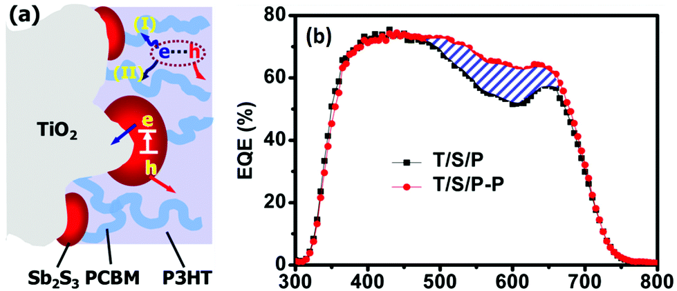 | ||
| Fig. 26 Schematic of the device structure (a). EQE spectra: the region marked by the blue lines is the EQE difference between the T/S/P–P and T/S/P samples (b). Reprinted from Chang et al.,39 with permission. | ||
The porously structured P3HT layer is expected to decrease the generated charge carrier recombination in P3HT and to decrease the hole transfer series resistance at the interface of P3HT/Au. Therefore, Lim et al.121 added AIBN as a nanopore-generating agent to the P3HT solution to create a porous P3HT layer in the FTO/bl-TiO2/mp-TiO2/Sb2S3/AIBN:P3HT/Au cell. A porously nanostructured P3HT film was formed by the thermal decomposition of AIBN. Compared to the reference cell, the device efficiency was improved by about 16%, exceeding 4.5%.
To enhance the P3HT hole transport mobility, Gamboa et al.67 mixed P3HT with NiOx nanoparticles (NiOx-NP) as an HTM. The solid Sb2S3-sensitized solar cells assembled from FTO/c-TiO2/mp-TiO2/Sb2S3/P3HT or P3HT:NiOx-NP/Ag delivered PCE from 2.22% to 3.34% using 2% NiOx-NP as the optimal concentration.
At a wavelength of 650 nm, the EQE of the Sb2S3 solar cells with P3HT usually exhibits a depression. PCPDTBT was used to overcome this shortcoming instead of P3HT. The mesoporous Sb2S3-sensitized FTO/c-TiO2/mp-TiO2/Sb2S3/PCPDTBT/Au solar cells did not exhibit a depression at a wavelength of 650 nm because the band gap of PCPDTBT was positioned at approximately 1.4 eV (Fig. 27). Accordingly, the device performance was superior to that of P3HT because of the higher current density that resulted from the decreased absorption loss. The best PCE reached 6.18%, with a Jsc of 15.3 mA cm−2, Voc of 616 mV, and FF of 65.7%.38
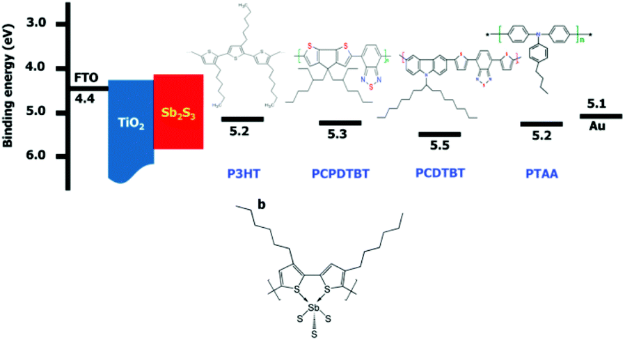 | ||
| Fig. 27 Energy level diagram of the corresponding materials used in devices. Reprinted from Im et al.,38 with permission. | ||
Considering the stability of solar cells, all-inorganic solar cell devices may be more desirable. CuSCN is the most commonly used inorganic HTM in Sb2S3 solar cells. CuSCN has p-type conductivity of 10−2 to 10−3 Ω−1 cm−1.122 The thiocyanate treatment increases the p-type conductivity of CuSCN. Itzhaik et al.31 reported Sb2S3/(KSCN)CuSCN solar cells with a PCE of 3.37%. These Sb2S3 solar cells were treated with KSCN solution before CuSCN deposition.79,108,123–125 After SCN− treatment, the phase changes of CuSCN were restricted, facilitating the diffusion of K+ ions into the CuSCN layer as a p-dopant to align the energy levels between Sb2S3 and the HTM layer. Moreover, K-doping passivated the surface trap states of CuSCN and resulted in decreased series resistance of the HTM and enhanced device performance. The treatment worked just as well in improving photovoltaic performance when carried out after CuSCN deposition (post-treatment).78 In addition, Tsujimoto et al.105 reported the effects of CuSCN thickness on the PCE of TiO2/Sb2S3/(KSCN)CuSCN cells. In the range of 0.68 to 1 μm, the PCE increased with increasing CuSCN thickness; the best efficiency of 3.71% was obtained with 1 μm thickness.
Among various inorganic semiconductors, V2O5 has received particular attention because of its outstanding physical properties, including suitable optical and electrical properties and ambient stability. It has been widely used as a hole transporter in organic photovoltaic devices. V2O5 served as a hole transporting material to substitute organic transporting materials for Sb2S3 solar cells. The PCE of the optimized device based on the Sb2S3/V2O5 heterojunction reached 4.8% (Fig. 28).55
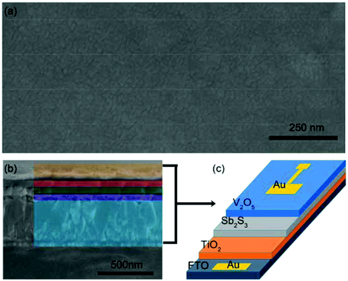 | ||
| Fig. 28 (a) SEM image of V2O5 film deposited on Sb2S3 and (b) cross-sectional SEM image of a complete device. (c) Illustration of the device with V2O5 as the hole transporting material. Reprinted from Zhang et al.,55 with permission. | ||
Inorganic p-type NiOx is believed to act as an efficient HTM for planar heterojunction Sb2S3 solar cells. The deposition of the NiOx HTM was thus conducted by spin-coating the nanoparticle ink in air, followed by low temperature annealing87 (Fig. 29). Upon O2 plasma treatment of the NiOx layer, the valence band maximum of NiOx shifted from −4.9 eV to −5.25 eV, giving rise to excellent energy-level alignment with Sb2S3 and the Au electrode. The device performance was thus significantly enhanced to 3.51% (Fig. 30).
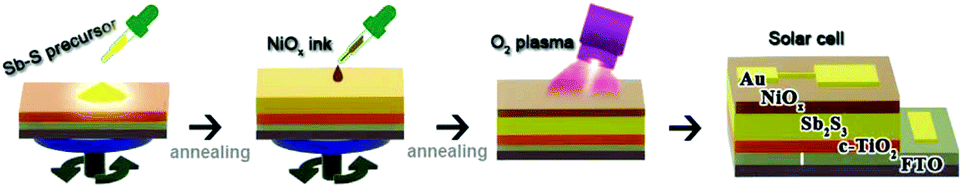 | ||
| Fig. 29 Schematic flow of fabricating the planar heterojunction Sb2S3 solar cell using NiOx hole transporting materials. Reprinted from Jin et al.,87 with permission. | ||
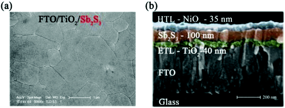 | ||
| Fig. 30 (a) Surface SEM image of the as-prepared Sb2S3 film deposited on FTO/TiO2. (b) Cross-sectional SEM image of the most efficient planar heterojunction Sb2S3 solar cell using the O2 plasma-treated NiOx HTM. Reprinted from Jin et al.,87 with permission. | ||
5. Conclusions and perspectives
Nearly thirty years have passed since the first report on Sb2S3 solar cells. Various device structures, mainly mesoporous sensitized solar cells and planar heterojunction solar cells, were extensively investigated. CBD, spin-coating, thermal evaporation, ALD, etc. have been used to achieve compact, uniform and impurity-free Sb2S3 absorbers. Simultaneously, novel ETM and HTM materials have been proposed and synthesized to assist the solar energy conversion and carrier transport processes. However, the PCE of Sb2S3 solar cells still lags greatly behind those of other thin film solar cells, such as cadmium telluride (CdTe) solar cells, copper indium gallium diselenide (CIGS) solar cells and perovskite solar cells. We suggest further improvement of Sb2S3 solar cells in the following aspects: (1) more knowledge of the defect properties both from theoretical and experimental aspects is needed. Theoretical simulation work on the electronic and band structures of Sb2S3 is rather limited; meanwhile, experimental characterization such as deep level transient spectrocopy, thermal admittance spectroscopy, and space charge limited current have been rarely reported. Good understanding and healing engineering of defects will play a key role in the development of Sb2S3 solar cells. (2) Novel synthesis of Sb2S3 nanostructured materials. To date, it is still difficult to synthesise high quality Sb2S3 nanostructures due to the ribbon-like (Sb4S6)n chains along the [001] direction. Despite this, we suggest that successful nano-synthesis of Sb2S3 will be benefical for solar cells, especially sensitized solar cells. The nuleation and growth process at suitable temperatures in organic solvent helps avoid the appearance of oxides, such as Sb2O3, which are usually formed in processes such as CBD. (3) Elucidating the device physics. Based on the knowledge of the material optoelectronic properties of Sb2S3, ETM and HTM, the device physics should be investigated either through numerical modelling or through capacitance–voltage studies, impedance spectroscopy, etc. Whether the p–i–n or p–n configuration is more favorable for performance and the role of the HTM must be clarified.Conflicts of interest
The authors declare that they have no conflict of interest.Acknowledgements
This work was supported by the National Key Research and Development Program of China (SQ2017YFGH001237), the Distinguished Youth Foundation of Anhui Province (1708085J09), and the Fundamental Research Funds for the Central Universities (JZ2018HGPB0276). The Key Lab of Photovoltaic and Energy Conservation Materials, Chinese Academy of Sciences is gratefully acknowledged by the authors.References
- A. E. Becquerel, Ann. Phys. Chem., 1839, 9, 145–149 Search PubMed.
- A. E. Becquerel, Ann. Phys. Chem., 1841, 54, 35–42 CrossRef.
- W. G. Adams and R. E. Day, Proc. R. Soc. London, 1877, 25, 113–117 CrossRef.
- T. K. Todorov, S. Singh, D. M. Bishop, O. Gunawan, Y. S. Lee, T. S. Gershon, K. W. Brew, P. D. Antunez and R. Haight, Nat. Commun., 2017, 8, 682 CrossRef PubMed.
- D. M. Chapin, C. S. Fuller and G. L. Pearson, J. Appl. Phys., 1954, 25, 676–677 CrossRef CAS.
- https://www.iea.org/topics/renewables/solar/ .
- https://www.nrel.gov/pv/cell-efficiency.html .
- X. M. Wang, R. F. Tang, C. Y. Wu, C. F. Zhu and T. Chen, J. Energy Chem., 2018, 27, 713–721 CrossRef.
- N. Yamada, K. Maruya, Y. Yamaguchi, X. Cao and Y. Ninomiya, Chem. Mater., 2015, 27, 8076–8083 CrossRef CAS.
- G. S. Selopal, R. Chahine, M. Mohammadnezhad, F. Navarro-Pardo, D. Benetti, H. G. Zhao, Z. M. Wang and F. Rosei, J. Power Sources, 2019, 436, 226849 CrossRef CAS.
- C. Qin, Y. C. Wang, Z. R. Lou, S. L. Yue, W. Z. Niu and L. P. Zhu, J. Alloys Compd., 2019, 779, 387–393 CrossRef CAS.
- P. Sinsermsuksakul, L. Z. Sun, S. W. Lee, H. H. Park, S. B. Kim, C. X. Yang and R. G. Gordon, Adv. Energy Mater., 2014, 1400496 CrossRef.
- Y. C. Choi, D. U. Lee, J. H. Noh, E. K. Kim and S. Il. Seok, Adv. Funct. Mater., 2014, 24, 3587–3592 CrossRef CAS.
- J. Zhang, R. Kondrotas, S. C. Lu, C. Wang, C. Chen and J. Tang, Sol. Energy, 2019, 96–101 CrossRef.
- A. Ennaoui, S. Fiechter, C. Pettenkofer, N. Alonso-Vante, K. Büker, M. Bronold, C. Höpfner and H. Tributsch, Sol. Energy Mater. Sol. Cells, 1993, 29, 289 CrossRef CAS.
- Y. X. Zhao and C. Burda, Energy Environ. Sci., 2012, 5, 5564–5576 RSC.
- K. W. Boer, J. Cryst. Growth, 1982, 59, 111 CrossRef.
- L. C. Olsen, F. W. Addis and W. Miller, Sol. Cells, 1982, 7, 247 CrossRef CAS.
- K. Hartman, J. L. Johnson, M. I. Bertoni, D. Recht, M. J. Aziz, M. A. Scarpulla and T. Buonassisi, Thin Solid Films, 2011, 519, 7421–7424 CrossRef CAS.
- M. Devika, N. K. Reddy, K. Ramesh, R. Ganesan, K. R. Gunasekhar, E. S. R. Gopal and K. T. R. Reddy, J. Electrochem. Soc., 2007, 154, H67–H73 CrossRef CAS.
- B. B. Nayak, H. N. Acharya, T. K. Chaudhuri and G. B. Mitra, Thin Solid Films, 1982, 92, 309–314 CrossRef CAS.
- W. Shockley and H. J. Queisser, J. Appl. Phys., 1961, 32, 510–519 CrossRef CAS.
- S. Rühle, Sol. Energy, 2016, 130, 139–147 CrossRef.
- Z. Q. Li, X. Y. Liang, G. Li, H. X. Liu, H. Y. Zhang, J. X. Guo, J. W. Chen, K. Shen, X. Y. San, W. Yu, R. E. I. Schropp and Y. H. Mai, Nat. Commun., 2019, 10, 125 CrossRef PubMed.
- A. D. Vos, J. Phys. D: Appl. Phys., 1980, 13, 839–846 CrossRef.
- M. Y. Versavel and J. A. Haber, Thin Solid Films, 2007, 515, 7171 CrossRef CAS.
- X. M. Wang, J. M. Li, W. F. Liu, S. F. Yang, C. F. Zhu and T. Chen, Nanoscale, 2017, 9, 3386–3390 RSC.
- R. F. Tang, X. M. Wang, C. H. Jiang, S. Li, W. F. Liu, H. X. Ju, S. F. Yang, C. F. Zhu and T. Chen, ACS Appl. Mater. Interfaces, 2018, 10, 30314–30321 CrossRef CAS PubMed.
- O. Savadogo and K. C. Mandal, J. Electrochem. Soc., 1992, 139, L16–L18 CrossRef CAS.
- O. Savadogo and K. C. Mandal, Appl. Phys. Lett., 1993, 63, 228–230 CrossRef CAS.
- Y. Itzhaik, O. Niitsoo, M. Page and G. Hodes, J. Phys. Chem. C, 2009, 113, 4254–4256 CrossRef CAS.
- O. Savadogo and K. C. Mandal, J. Electrochem. Soc., 1994, 141, 2871–2877 CrossRef CAS.
- S. Messina, M. T. S. Nair and P. K. Nair, Thin Solid Films, 2009, 517, 2503–2507 CrossRef CAS.
- K. F. Abd-El-Rahman and A. A. A. Darwish, Curr. Appl. Phys., 2011, 11, 1265–1268 CrossRef.
- D. H. Kim, S. J. Lee, M. S. Park, J. K. Kang, J. H. Heo, S. H. Im and S. J. Sung, Nanoscale, 2014, 6, 14549–14554 RSC.
- C. H. Jiang, R. F. Tang, X. M. Wang, H. X. Ju, G. Chen and T. Chen, Sol. RRL, 2019, 3, 1800272 CrossRef.
- J. A. Chang, J. H. Rhee, S. H. Im, Y. H. Lee, H. j. Kim, S. Il. Seok, M. K. Nazeeruddin and M. Gratzel, Nano Lett., 2010, 10, 2609–2612 CrossRef CAS PubMed.
- S. H. Im, C. S. Lim, J. A. Chang, Y. H. Lee, N. Maiti, H. J. Kim, Md. K. Nazeeruddin, M. Grätzel and S. Il Seok, Nano Lett., 2011, 11, 4789–4793 CrossRef CAS PubMed.
- J. A. Chang, S. H. Im, Y. H. Lee, H. Kim, C. S. Lim, J. H. Heo and S. Il Seok, Nano Lett., 2012, 12, 1863–1867 CrossRef CAS PubMed.
- J. C. Cardoso, C. A. Grimes, X. Feng, X. Y. Zhang, S. Komarneni, M. V. B. Zanonid and N. Z. Bao, Chem. Commun., 2012, 48, 2818–2820 RSC.
- R. F. Tang, X. M. Wang, C. H. Jiang, S. A. Li, G. S. Jiang, S. F. Yang, C. F. Zhu and T. Chen, J. Mater. Chem. A, 2018, 6, 16322–16327 RSC.
- J. H. Rhee, C.-C. Chung and E. W.-G. Diau, NPG Asia Mater., 2013, 5, e68 CrossRef CAS.
- Z. X. Pan, H. S. Rao, I. M. Seró, J. Bisquert and X. H. Zhong, Chem. Soc. Rev., 2018, 47, 7659–7702 RSC.
- Q. Jiang, Y. Zhao, X. W. Zhang, X. L. Yang, Y. Chen, Z. Chu, Q. F. Ye, X. X. Li, Z. G. Yin and J. B. You, Nat. Photonics, 2019, 13, 460–466 CrossRef CAS.
- R. Kondrotas, C. Chen and J. Tang, Joule, 2018, 2, 1–22 CrossRef.
- B. Chen, P. N. Rudd, S. Yang, Y. B. Yuan and J. S. Huang, Chem. Soc. Rev., 2019, 48, 3842–3867 RSC.
- S. J. Yuan, H. Deng, X. K. Yang, C. Hu, J. Khan, W. N. Ye, J. Tang and H. S. Song, ACS Photonics, 2017, 4, 2862–2870 CrossRef CAS.
- H. Deng, Y. Y. Zeng, M. Ishaq, S. J. Yuan, H. Zhang, X. K. Yang, M. M. Hou, U. Farooq, J. L. Huang, K. W. Sun, R. Webster, H. Wu, Z. H. Chen, F. Yi, H. S. Song, X. J. Hao and J. Tang, Adv. Funct. Mater., 2019, 1901720 CrossRef.
- V. T. Chebrolua and H.-J. Kim, J. Mater. Chem. C, 2019, 7, 4911–4933 RSC.
- G. Hodes and D. Cahen, Acc. Chem. Res., 2012, 45, 705–713 CrossRef CAS PubMed.
- P. V. Kamat, J. A. Christians and J. G. Radich, Langmuir, 2014, 30, 5716–5725 CrossRef CAS PubMed.
- Y. C. Choi and S. Il. Seok, Adv. Funct. Mater., 2015, 25, 2892–2898 CrossRef CAS.
- E. K. Gil, S. J. Lee, S. J. Sung, K. Y. Cho and D.-H. Kim, J. Nanosci. Nanotechnol., 2016, 16, 10763 CrossRef CAS.
- S. J. Sung, E. K. Gil, S. J. Lee, Y. C. Choi, K. J. Yang, J. K. Kang, K. Y. Cho and D.-H. Kim, J. Ind. Eng. Chem., 2017, 56, 196–202 CrossRef CAS.
- L. J. Zhang, C. H. Jiang, C. Y. Wu, H. X. Ju, G. S. Jiang, W. F. Liu, C. F. Zhu and T. Chen, ACS Appl. Mater. Interfaces, 2018, 10, 27098–27105 CrossRef CAS PubMed.
- C. P. Liu, Z. H. Chen, H. E. Wang, S. K. Jha, W. J. Zhang, I. Bello and J. A. Zapien, Appl. Phys. Lett., 2012, 100, 243102 CrossRef.
- C. P. Liu, H. E. Wang, T. W. Ng, Z. H. Chen, W. F. Zhang, C. Yan, Y. B. Tang, I. Bello, L. Martinu, W. J. Zhang and S. K. Jha, Phys. Status Solidi B, 2012, 249, 627–633 CrossRef CAS.
- X. Chen, Z. Q. Li, H. B. Zhu, Y. Wang, B. L. Liang, J. W. Chen, Y. Xua and Y. H. Mai, J. Mater. Chem. C, 2017, 5, 9421–9428 RSC.
- C. F. Lan, G. X. Liang, H. B. Lan, H. X. Peng, Z. H. Su, D. P. Zhang, H. B. Sun, J. T. Luo and P. Fan, Phys. Status Solidi RRL, 2018, 12, 1800025 CrossRef.
- H. Wedemeyer, J. Michels, R. Chmielowski, S. Bourdais, T. Muto, M. Sugiura, G. Dennlerb and J. Bachmann, Energy Environ. Sci., 2013, 6, 67–71 RSC.
- H. J. Jo, S. H. Kim and J. S. Kim, J. Korean Phys. Soc., 2016, 69, 541–546 CrossRef.
- H. W. Lei, T. H. Lin, X. R. Wang, S. Zhang, Q. L. Cheng, X. J. Chen, Z. J. Tan and J. J. Chen, Mater. Lett., 2018, 233, 90–93 CrossRef CAS.
- R. Parize, O. A. Katerski, I. Gromyko, L. Rapenne, H. Roussel, E. Kärber, E. Appert, M. Krunks and V. Consonni, J. Phys. Chem. C, 2017, 121, 9672–9680 CrossRef CAS.
- X. Zhang, S. Yoshioka, N. Loew and M. Ihara, ECS Trans., 2014, 64, 1–13 CrossRef CAS.
- C. H. Gao, J. L. Huang, H. X. Li, K. W. Sun, Y. Q. Lai, M. Jia, L. X. Jiang and F. Y. Liu, Ceram. Int., 2019, 45, 3044–3051 CrossRef CAS.
- C. F. Lan, J. T. Luo, H. B. Lan, B. Fan, H. X. Peng, J. Zhao, H. H. Sun, Z. H. Zheng, G. X. Liang and P. Fan, Materials, 2018, 11, 355 CrossRef PubMed.
- R. A. M. Gamboa, O. A. Jaramillo-Quintero, Y. A. A. Altamirano, M. O. Concha-Guzmán and M. E. Rincón, J. Colloid Interface Sci., 2019, 535, 400–407 CrossRef PubMed.
- S. M. Pawar, B. S. Pawar, J. H. Kim, O.-S. Joo and C. D. Lokhande, Curr. Appl. Phys., 2011, 11, 117–161 CrossRef.
- G. Hodes, Phys. Chem. Chem. Phys., 2007, 9, 2181–2196 RSC.
- C. D. Lokhande, Mater. Chem. Phys., 1991, 27, 1–43 CrossRef CAS.
- O. Savadogo and K. C. Mandal, Sol. Energy Mater. Sol. Cells, 1992, 26, 117–136 CrossRef CAS.
- O. Savadogo and K. C. Mandal, J. Phys. D: Appl. Phys., 1994, 27, 1070–1075 CrossRef CAS.
- S. Messina, M. T. S. Nair and P. K. Nair, Thin Solid Films, 2007, 515, 5777–5782 CrossRef CAS.
- E. Zimmermann, T. Pfadler, J. Kal, J. A. Dorman, D. Sommer, G. Hahn, J. Weickert and L. Schmidt-Mende, Adv. Sci., 2015, 2, 1500059 CrossRef PubMed.
- G. Hodes, J. Phys. Chem. C, 2008, 112, 17778–17787 CrossRef CAS.
- E. L. Gui, A. M. Kang, S. S. Pramana, N. Yantara, N. Mathews and S. Mhaisalkar, J. Electrochem. Soc., 2012, 159, B247–B250 CrossRef CAS.
- K. C. Gödel, B. Roose, A. Sadhanala, Y. Vaynzof, S. K. Pathake and U. Steiner, Phys. Chem. Chem. Phys., 2017, 19, 1425–1430 RSC.
- Y. Itzhaik, T. Bendikov, D. Hines, P. V. Kamat, H. Cohen and G. Hodes, J. Phys. Chem. C, 2016, 120, 31–41 CrossRef CAS.
- M. T. S. Nair, Y. Peña, J. Campos, V. M. García and P. K. Nair, J. Electrochem. Soc., 1998, 145, 2113–2120 CrossRef CAS.
- K. C. Gödel, Y. C. Choi, B. Roose, A. Sadhanala, H. J. Snaith, S. Il. Seok, U. Steiner and S. K. Pathak, Chem. Commun., 2015, 51, 8640–8643 RSC.
- K. Norrman, A. Ghanbari-Siahkali and N. B. Larsen, Annu. Rep. Prog. Chem., Sect. C: Phys. Chem., 2005, 101, 174–201 RSC.
- M. Pichumani, P. Bagheri, K. M. Poduska, W. González-Viñasa and A. Yethiraj, Soft Matter, 2013, 9, 3220–3229 RSC.
- I. A. Howard, T. Abzieher, I. M. Hossain, H. Eggers, F. Schackmar, S. Ternes, B. S. Richards, U. Lemmer and U. W. Paetzold, Adv. Mater., 2019, 31, 1806702 CrossRef PubMed.
- A. Kojima, K. Teshima, Y. Shirai and T. Miyasaka, J. Am. Chem. Soc., 2009, 131, 6050–6051 CrossRef CAS PubMed.
- Y. Cao, N. Wang, H. Tian, J. S. Guo, Y. Q. Wei, H. Chen, Y. F. Miao, W. Zou, K. Pan, Y. R. He, H. Cao, Y. Ke, M. M. Xu, Y. Wang, M. Yang, K. Du, Z. W. Fu, D. C. Kong, D. X. Dai, Y. Z. Jin, G. Q. Li, H. Li, Q. M. Peng, J. P. Wang and W. Huang, Nature, 2018, 562, 249–253 CrossRef PubMed.
- K. B. Lin, J. Xing, L. N. Quan, F. P. G. de Arquer, X. W. Gong, J. X. Lu, L. Q. Xie, W. J. Zhao, D. Zhang, C. Z. Yan, W. Q. Li, X. Y. Liu, Y. Lu, J. Kirman, E. H. Sargent, Q. H. Xiong and Z. H. Wei, Nature, 2018, 562, 245–248 CrossRef CAS PubMed.
- X. Jin, Y. Yuan, C. H. Jiang, H. X. Ju, G. S. Jiang, W. F. Liu, C. F. Zhu and T. Chen, Sol. Energy Mater. Sol. Cells, 2018, 185, 542–548 CrossRef CAS.
- S. A. Li, Y. Zhang, R. F. Tang, X. M. Wang, T. Zhang, G. S. Jiang, W. F. Liu, C. F. Zhu and T. Chen, ChemSusChem, 2018, 11, 3208–3214 CrossRef CAS PubMed.
- L. J. Zhang, C. Y. Wu, W. F. Liu, S. F. Yang, M. T. Wang, T. Chen and C. F. Zhu, J. Mater. Chem. A, 2018, 6, 21320–21326 RSC.
- L. Zheng, K. J. Jiang, J. H. Huang, Y. Zhang, B. Bao, X. Q. Zhou, H. J. Wang, B. Guan, L. M. Yang and Y. L. Song, J. Mater. Chem. A, 2017, 5, 4791–4796 RSC.
- Y. Shirasaki, G. J. Supran, M. G. Bawendi and V. Bulović, Nat. Photonics, 2013, 7, 13–23 CrossRef CAS.
- G. H. Carey, A. L. Abdelhady, Z. J. Ning, S. M. Thon, O. M. Bakr and E. H. Sargent, Chem. Rev., 2015, 115(23), 12732–12763 CrossRef CAS PubMed.
- W. Wang, F. Strössner, E. Zimmermann and L. Schmidt-Mende, Sol. Energy Mater. Sol. Cells, 2017, 172, 335–340 CrossRef CAS.
- D. Cope, U.S. Patent, 2875359, 1959 Search PubMed.
- E. Montrimas and A. Pažėra, Thin Solid Films, 1976, 34, 65–68 CrossRef CAS.
- J. Grigas, J. Meshkauska and A. Orliukas, Phys. Status Solidi A, 1976, 37, K39–K41 CrossRef CAS.
- Y. Osorio Mayon, T. P. White, R. Wang, Z. Yang and K. R. Catchpole, Phys. Status Solidi A, 2016, 213, 108–113 CrossRef CAS.
- L. Lee, J. Park, K. S. Han, R. S. Kumar and M. M. Sung, Appl. Surf. Sci., 2019, 476, 897–904 CrossRef CAS.
- J. Escorcia-García, D. Becerra, M. T. S. Nair and P. K. Nair, Thin Solid Films, 2014, 569, 28–34 CrossRef.
- M. Kamruzzaman, L. Chaoping, F. Yishu, A. K. M. Farid Ul Islam and J. A. Zapien, RSC Adv., 2016, 6, 99282–99290 RSC.
- H. Deng, S. J. Yuan, X. K. Yang, F. S. Cai, C. Hu, K. K. Qiao, J. Zhang, J. Tang, H. S. Song and Z. B. He, Mater. Today Energy, 2017, 3, 15–23 CrossRef.
- Y. W. Yin, C. Y. Wu, R. F. Tang, C. H. Jiang, G. S. Jiang, W. F. Liu, T. Chen and C. F. Zhu, Sci. Bull., 2019, 64, 136–141 CrossRef CAS.
- H. W. Lei, G. Yang, Y. X. Guo, L. B. Xiong, P. L. Qin, X. Dai, X. L. Zheng, W. J. Ke, H. Tao, Z. Chen, B. Li and G. J. Fang, Phys. Chem. Chem. Phys., 2016, 18, 16436–16443 RSC.
- S. J. Yuan, H. Deng, D. D. Dong, X. K. Yang, K. K. Qiao, C. Hu, H. B. Song, H. S. Song, Z. B. He and J. Tang, Sol. Energy Mater. Sol. Cells, 2016, 157, 887–893 CrossRef CAS.
- K. Tsujimoto, D. C. Nguyen, S. Ito, H. Nishino, H. Matsuyoshi, A. Konno, G. R. A. Kumara and K. Tennakone, J. Phys. Chem. C, 2012, 116, 13465–13471 CrossRef CAS.
- Q. Ye, Y. F. Xu, W. Y. Chen, S. F. Yang, J. Zhu and J. Weng, Appl. Surf. Sci., 2018, 440, 294–299 CrossRef CAS.
- Y. F. Xu, W. Y. Chen, X. H. Ding, X. Pan, L. H. Hu, S. F. Yang, J. Zhu and S. Y. Dai, Inorg. Chem. Front., 2018, 5, 1370–1377 RSC.
- Y. F. Xu, W. Y. Chen, L. H. Hu, X. Pan, S. F. Yang, Q. Shen and J. Zhu, J. Alloys Compd., 2019, 784, 947–953 CrossRef CAS.
- S. Gubbala, V. Chakrapani, V. Kumar and M. K. Sunkara, Adv. Funct. Mater., 2008, 18, 2411–2418 CrossRef CAS.
- Z. M. Jarzebski and J. P. Marton, J. Electrochem. Soc., 1976, 123, 299C–310C CrossRef CAS.
- M. S. Arnold, P. Avouris, Z. W. Pan and Z. L. Wang, J. Phys. Chem. B, 2003, 107, 659–663 CrossRef CAS.
- Ü. Özgür, Ya. I. Alivov, C. Liu, A. Teke, M. A. Reshchikov, S. Doğan, V. Avrutin, S.-J. Cho and H. Morkoç, J. Appl. Phys., 2005, 98, 041301 CrossRef.
- W. U. Huynh, J. J. Dittmer and A. P. Alivisatos, Science, 2002, 295, 2425–2427 CrossRef CAS PubMed.
- S. J. Moon, Y. Itzhaik, J. H. Yum, S. M. Zakeeruddin, G. Hodes and M. Grätzel, J. Phys. Chem. Lett., 2010, 1, 1524–1527 CrossRef CAS.
- P. P. Boix, Y. H. Lee, F. Fabregat-Santiago, S. H. Im, I. Mora-Sero, J. Bisquert and S. I. Seok, ACS Nano, 2012, 6, 873–880 CrossRef CAS PubMed.
- T. Muto, G. Larramona and G. Dennler, Appl. Phys. Express, 2013, 6, 072301 CrossRef.
- T. Fukumoto, T. Moehl, Y. Niwa, M. K. Nazeeruddin, M. Grätzel and L. Etgar, Adv. Energy Mater., 2013, 3, 29–33 CrossRef CAS.
- C. C. Chung, T. W. Tsai, H. P. Wu and E. W. G. Diau, J. Phys. Chem. C, 2017, 121(34), 18472–18479 CrossRef CAS.
- Y. Q. Xiao, C. L. Li, X. Y. Tan, L. Zhang, Y. J. Zhong and H. W. Zhu, Sol. RRL, 2017, 1, 1700135 CrossRef.
- J. Burschka, A. Dualeh, F. Kessler, E. Baranoff, N.-L. Cevey-Ha, C. Y. Yi, M. K. Nazeeruddin and M. Grätzel, J. Am. Chem. Soc., 2011, 133, 18042–18045 CrossRef CAS PubMed.
- C.-S. Lim, S. H. Im, J. A. Chang, Y. H. Lee, H.-J. Kim and S. I. Seok, Nanoscale, 2012, 4, 429–432 RSC.
- C. Rost, I. Sieber, C. Fischer, M. C. Lux-Steiner and R. Könenkamp, Mater. Sci. Eng., B, 2000, 69–70, 570–573 CrossRef.
- Y. Itzhaik, G. Hodes and H. Cohen, J. Phys. Chem. Lett., 2011, 2, 2872–2876 CrossRef CAS.
- P. P. Boix, G. Larramona, A. Jacob, B. Delatouche, I. Mora-Sero and J. Bisquert, J. Phys. Chem. C, 2012, 116, 1579–1587 CrossRef CAS.
- J. A. Christians and P. V. Kamat, ACS Nano, 2013, 7, 7967–7974 CrossRef CAS PubMed.
| This journal is © the Partner Organisations 2019 |