
Laser-induced graphene-based digital microfluidics (gDMF): a versatile platform with sub-one-dollar cost†
Ke
Liu
a,
Yu
He
 ab,
Zefan
Lu
a,
Qiudi
Xu
a,
Lan
Wang
a,
Zhongxuan
Liu
a,
Jeremy
Khou
a,
Jiaming
Ye
c,
Chong
Liu
d and
Tao
Zhang
*ab
ab,
Zefan
Lu
a,
Qiudi
Xu
a,
Lan
Wang
a,
Zhongxuan
Liu
a,
Jeremy
Khou
a,
Jiaming
Ye
c,
Chong
Liu
d and
Tao
Zhang
*ab
aResearch Center for Analytical Instrumentation, Institute of Cyber-Systems and Control, College of Control Science and Engineering, Zhejiang University, Hangzhou 310023, China. E-mail: zhtao@zju.edu.cn
bResearch Center for Analytical Instrumentation and Intelligent Systems, Huzhou Institute of Zhejiang University, Huzhou 313002, China
cTinkerbio Biotechnology Co., Ltd, Hangzhou 310023, China
dDepartment of Neurobiology, Department of Neurosurgery of Second Affiliated Hospital, School of Medicine, Zhejiang University, Hangzhou 310023, China
First published on 9th May 2024
Abstract
Digital microfluidics (DMF), is an emerging liquid-handling technology, that shows promising potential in various biological and biomedical applications. However, the fabrication of conventional DMF chips is usually complicated, time-consuming, and costly, which seriously limits their widespread applications, especially in the field of point-of-care testing (POCT). Although the paper- or film-based DMF devices can offer an inexpensive and convenient alternative, they still suffer from the planar addressing structure, and thus, limited electrode quantity. To address the above issues, we herein describe the development of a laser-induced graphene (LIG) based digital microfluidics chip (gDMF). It can be easily made (within 10 min, under ambient conditions, without the need of costly materials or cleanroom-based techniques) by a computer-controlled laser scribing process. Moreover, both the planar addressing DMF (pgDMF) and vertical addressing DMF (vgDMF) can be readily achieved, with the latter offering the potential of a higher electrode density. Also, both of them have an impressively low cost of below $1 ($0.85 for pgDMF, $0.59 for vgDMF). Experiments also show that both pgDMF and vgDMF have a comparable performance to conventional DMF devices, with a colorimetric assay performed on vgDMF as proof-of-concept to demonstrate their applicability. Given the simple fabrication, low cost, full function, and the ease of modifying the electrode pattern for various applications, it is reasonably expect that the proposed gDMF may offer an alternative choice as a versatile platform for POCT.
1. Introduction
Digital microfluidics (DMF), based on electrowetting on dielectric (EWOD), is an emerging liquid-handling technology.1–3 By precisely manipulating discrete droplets on an electrode array, DMF can offer great benefits such as automation, programmability, integration, and dynamic configuration.4,5 With these advantages, DMF has become a promising platform for a wide variety of biological and biomedical applications, among which point-of-care testing (POCT) is one of the most important fields.6–8 To date, various POCT applications have been demonstrated on DMF devices, including detection of nucleic acids,8–11 immunoassay,12–15 and cell analysis.16–18 However, for nearly all of these application scenarios, the DMF chips are not only required to be fully functional to address complex tasks, but disposable to avoid cross-contamination. Therefore, both the functionality and affordability of the DMF should be carefully considered when using them in POCT.Conventional DMF chips are usually fabricated in cleanroom facilities, where metal electrodes are patterned on a glass substrate using expensive, time-consuming, and complicated techniques, such as photolithography, etching, or sputtering.15,19–21 This adds significant cost and complexity to DMF device fabrication, thereby, impeding their wide applications in POCT. Another major problem with glass-based chips is that both the electrodes and the connecting wires are located in the same plane, which would seriously limit the electrode quantity and the chip functionalities. To address these issues, printed circuit board (PCB)-based chips have been widely used as an alternative.22–25 The merits of these chips include: the manufacturing of PCBs is very mature with relatively low cost; meanwhile, the multi-layer PCB structure enables the vertical addressing of the electrodes, therefore, a higher electrode density can be achieved as there is no need to route connecting wires on the same plane. However, the PCB chips are often criticized for their unreliable droplet movement due to the channels between the electrodes.26 The thickness of the top copper layer can reach tens of microns, causing poor surface evenness. Moreover, the final price of the PCB chips is highly dependent on the machining precision and the scale of production. Also, the usage of PCBs as disposable medical consumables will inevitably generate more e-waste, and thus, increasing the environmental burdens. Very recently, an emerging DMF device based on thin film transistors (TFTs) has also been reported.27–29 Typically, it involves an active matrix of thousands of electrodes, with each electrode able to be addressed individually. Such features have promptly made the TFT-based DMF device a very hot topic, which has gained extensive interest in recent years. However, the manufacturing of TFT usually involves a series of advanced semiconductor technologies, e.g., multilayer photolithography, etching, sputtering, and film deposition. While the industrial production is very mature, it is still inaccessible for most everyday users, and the device cost for the POCT applications remain to be proven.26,30
In order to obtain affordable DMF devices, inkjet printing31–35 and screen printing36,37 are also used to pattern the electrodes on paper (paper-based DMF, pDMF) or polymer films (film-based DMF, fDMF). While these techniques can offer a simple, rapid fabrication process with a relatively low cost, the proposed pDMF and fDMF chips often share the same planar structures, and thus, similar limitations, with the glass-based chips. To solve this problem, a double-sided electro-hydrodynamic jet printing38 method has been proposed for the fabrication of the vertical addressed pDMF. However, the fabrication process becomes more complicated, involving multiple printing steps. This is mainly because the vertical connecting spots need to be printed onto both sides of the paper, and the electrodes and connecting lines are on the top and bottom surfaces, respectively. A one-plane vertical addressing DMF chip based on polymer film has been reported,30 however, cleanroom-based techniques, e.g., photolithography, are still needed to pattern the electrodes, and its connections with the PCB interface rely on a vacuum manifold, which leads to complex peripherals. Therefore, it remains an urgent demand to develop alternative DMF devices that can comprehensively address the above issues.
To this end, we herein propose laser-induced graphene (LIG)-based digital microfluidics (gDMF). The LIG is a one-step approach to produce graphene by using a CO2 laser,39–41 which has been widely used to form flexible sensors42 and supercapacitors.43 The infrared laser can readily convert sp3 to sp2 carbon bonds, resulting in the formation of LIG materials.44 By taking advantage of the LIG technique, the DMF electrodes of any shape can be directly made on a polymer (e.g., polyimide, PI) film by computer-controlled laser scribing (Fig. 1A). The whole process can be performed under ambient conditions, without the need of costly materials or cleanroom-based techniques, which can significantly reduce the chip cost, and shortens the production cycles. Moreover, both the planar addressing DMF chip (pgDMF, Fig. 1C) and the vertical addressing DMF chip (vgDMF, Fig. 1E) can be readily achieved. For the pgDMF, the driving electrodes, connecting wires, and contact pads for external connections can all be patterned on the same plane within 10 min. Moreover, a composite hydrophobic–dielectric (CHD) layer has been further developed, which features both high permittivity and strong hydrophobicity, and can be rapidly formed in a single-step by UV irradiation. For the vgDMF, only the electrodes need to be patterned on one side of the PI film, and the other film side can directly serve as the dielectric layer thanks to its relatively high permittivity (εr ≈ 3.1).45,46 It is therefore even more simple and quicker than the pgDMF fabrication, easily meets the demand of high electrode density and low cost. As estimated previously, the costs of the pgDMF and vgDMF chips are both below $1 ($0.85 for pgDMF, $0.59 for vgDMF), and, due to the flexibility of the LIG process, the electrode pattern can be changed at will to suit various applications. We therefore reasonably envision that the proposed gDMF may offer an alternative choice as a low-cost and versatile platform for POCT.
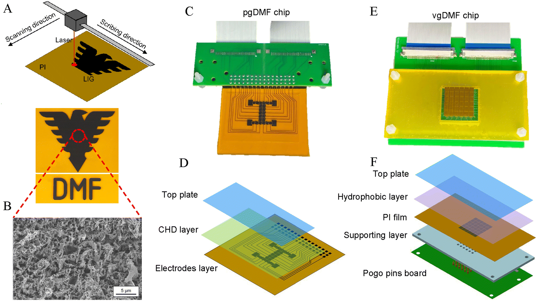 | ||
| Fig. 1 (A) Schematic illustration of laser-induced graphene (LIG) fabrication. (B) SEM image of the LIG formed. (C) Photograph, and (D) exploded view of the planar addressing of gDMF (pgDMF). (E) Photograph, and (F) exploded view of the vertical addressing of gDMF (vgDMF). | ||
2. Experimental
2.1 Materials and reagents
The polyimide (PI) films, with thicknesses of 40 μm and 80 μm, were purchased from Zhongshan Chenxi Technologies Co., Ltd (Zhongshan, China). The poly(methyl methacrylate) (PMMA) sheet and double-sided tape were obtained from YoungChip Technologies Co., Ltd (Hangzhou, China). Indium tin oxide (ITO) conductive film was purchased from Shenzhen Tianmidun Electronics Co., Ltd (Shenzhen, China). pentaerythritol tetrakis mercaptoacetate (PETMP), triallyl-1,3,5-triazine-2,4,6-trione (TATATO), and 2-hydroxy-2-methylpropiophe-none (HMPP) were obtained from Aladdin (Shanghai, China). The fluorinated anti-fouling agent (FAA) was obtained from Shin-Etsu Chemical Co., Ltd. The fluorinated dispersion PyFlon was obtained from Shanghai FluoroLuster Materials Co., Ltd (Shanghai, China). Glucose oxidase (GOx), horseradish peroxidase (HRP), 4-aminoantipyrine (4-AAP), 3-(N-ethyl-3-methylanilino)propanesulfonic acid sodium salt (TOPS), and glucose solution were obtained from Sigma-Aldrich. The fluorinated oil FC-40 and silicone oil PMX-200 were obtained from 3M and Dow, respectively.2.2 LIG electrodes fabrication
A commercial laser scriber (YoungLaser-V12, YoungChip, China), with a maximum power of 30 W and a maximum scanning speed of 1500 mm s−1, was used to fabricate the LIG electrodes. Patterns were designed using AutoCAD and uploaded into the laser controller. All the LIG were scribed at the optimal laser parameters, i.e., 10% laser power, 9% scanning speed, and 750 dots per inch (DPI). Afterwards, the formed LIG was washed with ethanol and blown dry with air. In order to assess the LIG scribing resolution, a strip-containing pattern with a different designed gap width (DGW) was scribed in both the vertical and horizontal directions. Then, the actual gap width (AGW) was measured using a microscope (Nexcope, China), and the resistance between adjacent electrodes was measured by using a digital multimeter (990C, Victor, China).2.3 The CHD layer characterization and operation
First, the thiol-ene (TE) precursor (74 wt% PETMP, 25 wt% TATATO and 1 wt% HMPP as photo initiator) was prepared. Then, different concentrations of FAA (from 1 wt% to 9 wt%) were added and mixed thoroughly. Each resultant mixture was cast into a film (250 μm), and cured by UV exposure (365 nm, 45 mW cm−2) for 3 s. The film hydrophobicity was examined on a contact angle measuring instrument (Dropmeter A-100P, Haishumaishi Scientific Testing, China). Each film was also cut into a circle of 2 mm diameter for relative permittivity measurement on a broadband dielectric impedance spectrometer (Concept 40, Novocontrol Technologies, Germany).2.4 The pgDMF chip fabrication
The electrode pattern of the pgDMF chip was designed using AutoCAD, as shown in Fig. S1A.† Firstly, for the bottom plate, the PI film (80 μm, with adhesive on one side) was attached to a PMMA substrate and patterned using the laser scriber mentioned previously to obtain the LIG electrodes (Movie S1†), and this was followed by washing with ethanol, and then blown dry with air to avoid potential connections between the adjacent electrodes. Then, the CHD material, containing 95 wt% TE and 5 wt% FAA (∼1.65 mL), was cast onto the LIG electrodes, and covered by a perfluorodecyltriethoxysilane (PFDTES) treated glass slide, with a spacer of 60 μm thickness, to form a film. After UV exposure (365 nm, 45 mW cm−2, 3 s), the top glass was removed. For the top plate, a 10 μm-thick CHD layer was formed on the ITO film (attached to a PMMA substrate) using a similar method. Finally, the two plates were assembled together to form the pgDMF device, with a 350 μm-thick double-sided tape as a spacer, at the same time, sealing around the device. For droplet manipulation, the chip was connected to a homemade control system using a pogo pin board, and filled with fluorinated oil FC-40. Because FAA is a photoreactive material that can stably crosslink with the thiol-ene substrate, the hydrophobicity of the CHD layer would not be destroyed by the fluorinated oil. The applied voltage was 110–200 Vrms (100 Hz), and a digital camera (E80, Canon) to observe the movement of the droplets.2.5 vgDMF chips fabrication and operation
A proof-of-concept vgDMF pattern containing a 6 × 6 electrode (3 × 3 mm) array with 180 μm electrode gaps was designed using AutoCAD, as shown in Fig. S1B-I and II.† For the bottom plate, the PI film (40 μm) was firstly patterned using a nearly identical protocol as mentioned above to obtain the LIG electrodes. Then, a supporting layer was prepared by attaching the double-sided tape on a PMMA sheet, and then scribed on the laser scriber (power 85%, speed 1%) to make the connection holes (Fig. S1B-II†). Afterwards, the PI film was adhered to the supporting layer, with the patterned electrodes facing down, and aligned with the connection holes. The PyFlon was then coated on the PI surface as the hydrophobic layer, followed by 85 °C drying for 30 min. PyFlon is a fluorinated resin similar to Teflon AF, and can provide a satisfactory contact angle of ∼120° (Fig. S2†). For the top plate, PyFlon was coated on an ITO film and dried using the same method. The two plates were assembled together using a 350 μm-thick double-sided tape to form the final vgDMF device. For droplet manipulation, the chip was connected to a PCB board with pogo pins placed in the through-holes, and filled with silicone oil. Herein, the commonly used fluorinated oil was not applicable as it can dissolve the PyFlon layer. A voltage of 140–200 Vrms (100 Hz) was applied to manipulate the droplets on the vgDMF, and a digital camera (E80, Canon) was used to observe the movement of the droplets.2.6 Colorimetric analysis of the VgDMF chips
To demonstrate the applicability of our gDMF, a glucose assay based on Trinder's reaction47 was carried out on the vgDMF. Firstly, a reaction mixture was prepared, with GOx (12.5 U mL−1), HRP (2.5 U mL−1), 4-AAP (0.6 mg mL−1), and TOPS (1.6 mg mL−1) in DI water. Then, six glucose solutions at different concentrations (0.56 mM, 1.0 mM, 1.8 mM, 3.2 mM, 5.6 mM, 10 mM) were prepared by serial dilution. The on-chip assay was performed by merging a 9 μL droplet of glucose solution (or DI water used as a blank) and a 9 μL droplet of the reaction mixture on vgDMF. The merged droplet was then mixed and incubated under ambient temperature. A digital camera (E80, Canon) was used to record the reaction process. To maintain a constant lighting condition, a microscope LED ring light (SangNond, China) was fixed 7 cm above the chip. An area of 23 × 21 pixels was first extracted from each droplet image, and the average R, G, B data was used to calculate the distance between each droplet image, and a reference (the image obtained with 10 mM glucose at 250 s in this case), was then normalized, as the relative color change (RCC) value.3. Results and discussion
Whereas DMF is generally considered as a promising platform for a wide range of biological and biomedical applications, the fabrication of DMF devices remains a key challenge, which is impeding their large-scale production and widespread applications, especially in the field of POCT. This is mainly because of the complicated manufacturing process, cleanroom facilities/techniques dependence, and the resulting high cost. In order to address these issues, for the first time, we report a versatile and flexible DMF platform based on a laser-induced graphene (LIG) technique (Fig. 1). Herein, the LIG electrodes parameters were firstly optimized, and then based on this both the planar addressing and the vertical addressing DMF devices have been developed, and applied to a colorimetric assay of glucose as a proof-of-concept demonstration.3.1 Optimization of the LIG electrodes
The LIG electrodes were fabricated on PI film by using a laser scriber, which has a maximum power of 30 W and maximum scanning speed of 1500 mm s−1. To stably generate the LIG electrodes, we firstly optimized the working parameters of the laser scriber. It was found that high quality LIG could be formed with a 10% laser power (3 W) and 9% scanning speed (135 mm s−1), with other parameters such as scribing resolution having little effect on the LIG fabrication. The generated LIG was characterized with scanning electron microscopy (SEM) image (Fig. 1B) and Raman spectroscopy (Fig. S3†), both giving similar results to those of previous reports,39–41 thereby, verifying the successful generation of porous graphene. The LIG formed under optimal conditions was highly conductive with a sheet resistance of 30 Ω sq−1, which, was proven in our later work, to satisfy the requirements of DMF.After these basic optimizations, we further examined the electrode gap width because it is a key factor of DMF devices. Herein, a LIG pattern with multiple strips (Fig. 2A) was designed, with all of them having the same dimensions, but different designed gap widths (DGW) between each other, which increased from 100 μm to 200 μm with a step of 10 μm. Given that our laser scriber has an X–Y scanning mode, both the vertical and horizontal strip patterns were fabricated, which were used to assess the horizontal (X-direction) and vertical (Y-direction) resolution, respectively. Microscopic images and actual gap width (AGW) of the LIG patterns are shown in Fig. 2B and D. It was found that the AGW was always narrower than the DGW, resulting in three states between the adjacent electrodes, i.e., connected, semi-connected, and separated (Fig. 2C). For the vertical strip pattern (Fig. 2B-I and D-I), when the DGW is below 120 μm, only the connected states can be obtained, in which the LIG fully covers the gaps, causing adjacent electrodes to short-circuit. By further increasing the DGW to 130–140 μm, clear gaps without noticeable LIG begin to appear. In these cases, however, the resistance of tens to hundreds of kΩ can still be measured between neighbouring electrodes. This is probably because the invisible free graphene powder/fibers may exist in the gap region, causing the adjacent electrodes to be semi-connected. Although they can be removed by repeated cleaning, the process is cumbersome, and still has a risk of a short circuit occurring. When the DGW is set over 150 μm, the adjacent electrodes will show a separated state, i.e., electrical disconnection, which is a demanding requirement for DMF applications. Therefore, the minimum gap that is acceptable in the horizontal (X axis) direction is about 80 μm (AGW = 79.6 ± 3.3 μm, with a DGW set at 150 μm) under current conditions. Similar results have also been obtained for the vertical (Y axis) direction (Fig. 2B-II and -IID), which show a minimum AGW of about 110 μm (111.5 ± 5.1 μm) with the DGW set at 170 μm. A possible reason for this relatively poor resolution in the Y direction is that the LIG edge parallel to the laser scribing direction is easier to deform due to the thermal effects. Herein, for the sake of reliability and safety, we choose 180 μm as the DWG value in both the X and Y directions. This was also because it can offer similar AGWs in both directions (114.5 ± 5.1 μm and 115.8 ± 6.1 μm, respectively). Although a little bit compromised, the gaps obtained remain better than or comparable to those of the typical DMF chips, such as PCB chips (100–150 μm),26,30 pDMF chips (200–450 μm),38,48,49 and fDMF chips (60–90 μm).32
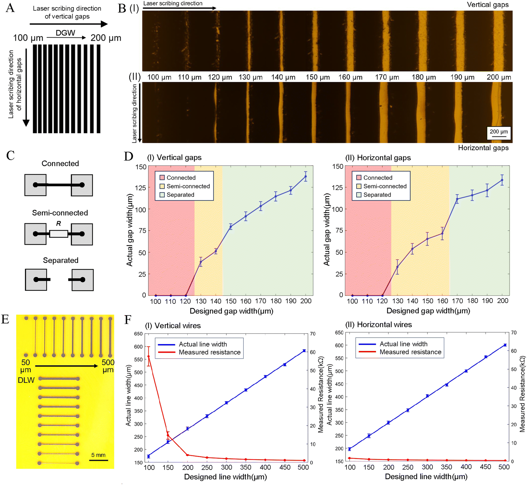 | ||
| Fig. 2 (A) The strip pattern for LIG electrode optimization, with a designed gap width (DGW) between adjacent strips increasing from 100 μm to 200 μm. (B) Microscopic images of the (I) vertical and (II) horizontal LIG strip patterns. (C) Schematic of the three states (connected, semi-connected, and separated) between the adjacent electrodes. (D) Relationship between the designed gap width (DGW) and actual gap width (AGW) of (I) vertical and (II) horizontal strips. (E) Photographs of the vertical and horizontal LIG wires. (F) Relationship between designed line width (DLW), actual line width (ALW), and measured resistance (MR) of the vertical (I) and horizontal (II) LIG wires. Error bars were obtained from 11 replicates. | ||
The connecting wires are also necessary elements especially for planar addressing DMF, and also have notable effects on device configuration and functions. Wide wires will not only waste the chip space and lead to difficulties in electrode arrangement, but also seriously affect the movement of the droplets. However, narrow LIG wires may result in high resistance or even open circuits. Therefore, their width has also been optimized in this work. Herein, both vertical and horizontal LIG wires were scribed (Fig. 2E), with the actual line width (ALW) and measured resistance (MR) shown in Fig. 2F. As can be seen in Fig. 2E, the LIG wire with a designed line width (DLW) of 50 μm cannot be formed in the vertical direction. By further increasing the DLW over 100 μm, clear LIG wires can be observed, with the ALW proportional to, and larger (∼80 μm), than the DLW (Fig. 2F-I). It was also found that the MRs dramatically decreased with the widening of the LIG wires, and were of the same order of magnitude (<10 kΩ) when the DLW is larger than 200 μm (Fig. 2F-I). For the horizontal wires, all the DLW values (including 50 μm) can lead to successful generation of the LIG wires (Fig. 2E), and likewise, the ALW values are proportional to, and larger (∼100 μm), than the DLW (Fig. 2F-II). However, their resistances were significantly smaller than those of the vertical wires of the same DLW values, which were all below 2 kΩ (Fig. 2F-II). Such a difference can be explained by the X–Y scribing process. Specifically, the vertical wires (perpendicular to laser scribing direction) need to undergo the Y-scanning process, which may result in certain discontinuous LIG at relatively small DLW values, thereby, leading to a higher resistance. In contrast, the horizontal wires (parallel with the scribing direction) suffer less from Y-scanning related discontinuities, and thus, show higher conductivity. Based on the above results, we chose 200 μm as the DLW value for both directions, which can balance the wire width and resistance requirements, and offers similar values for both vertical (ALW ∼281.3 ± 5.5 μm, MR ∼3.9 ± 0.2 kΩ cm−1) and horizontal (ALW ∼299.6 ± 5.6 μm, MR ∼0.9 ± 0.1 kΩ cm−1) wires.
3.2 Planar addressing gDMF (pgDMF) chip
To demonstrate the feasibility of the LIG-based digital microfluidics (gDMF), we first developed a planar addressing gDMF chip (pgDMF, Fig. 1C). As shown in Fig. 1D, it mainly consists of a bottom plate and a top plate, with detailed fabrication processes displayed in Fig. 3A. For the bottom plate, the LIG was first scribed on a PI film of 80 μm thick (Movie S1†). Here, the driving electrodes, the connecting wires, and the contact pads for external connections (Fig. S1A†) could all be patterned on the same plane in a single step. Plus, the whole process can be performed under ambient conditions within 10 min, without using any other costly materials or cleanroom-based techniques. This will significantly reduce the chip cost, and shorten the production cycle. For conventional DMF devices, an extra issue is that the dielectric and hydrophobic layers need to be formed successively, which usually involves complicated processes and expensive hydrophobic reagents (e.g., Teflon20 or CYTOP25). To address this issue, we further developed a composite hydrophobic dielectric (CHD) material by using a TE polymer and a fluorinated anti-fouling agent (FAA). As shown in Fig. 3B, the hydrophobicity of the TE film could be notably improved by an increase of the FAA concentration. The contact angle gradually increased from 72.8° (pure TE film) to ∼110° when the FAA concentration was raised to 5 wt%, and a higher FAA concentration did not show any more notable changes. Therefore, 5 wt% FAA was finally set as the optimized concentration in our later experiment in the interest of both the photocuring quality and cost control. After that, we further examined the permittivity of the cured CHD film. As shown in Fig. 3C, its relative permittivity (εr ≈ 6.5) is not only higher than that of the commonly used dielectric films (e.g., PDMS εr ≈ 2.8, SU-8 εr ≈ 3.0), but also the native TE film itself (εr ≈ 5.3). The above results indicate that the CHD film has both a strong hydrophobicity and high dielectricity, and thus, very suitable for DMF applications, i.e., a single CHD layer is adequate as a substitute for the conventional two-layer structure. Additional advantages also include that the high dielectric constant allows us to use a relatively thick CHD layer (∼60 μm in this case), which could fill up the channels between the LIG electrodes, leading to an even surface which avoids droplets from getting stuck, as traditional PCB chips did. Moreover, it can be readily formed by a simple single-step UV curing method under ambient conditions, without the need of expensive reagents and time-consuming processes. This could further simplify the fabrication process, and lower the ultimate chip cost. It is estimated that the total material cost of our pgDMF chip (including top and bottom plates) is ∼$0.85 (see Table S1† for details), thereby offering good affordability for POCT applications. To further examine the functionality of our pgDMF chip, droplet manipulations were performed on it. The results show that all the basic operations of DMF, including droplet dispensing, moving, splitting, and merging, can be realized with a 0.01 M PBS buffer (Fig. 3D, Movie S2†), and no droplet residue was observed after movement of 100 steps (Fig. S4†). It should be noted, that the CHD layer is nearly transparent, and the black colored LIG electrodes can be seen through that layer. It is also found that a relatively wide voltage range (110–200 V, 100 Hz) can be applied. Further increasing of the voltage may lead to a high risk of the CHD layer breaking down. The droplet movement speeds under different driving voltages are shown in Fig. 3E, which are comparable to those of traditional DMF devices under similar voltages.10,50 In addition, we further examined the manipulation of the PCR amplification buffer and 1 M MgCl2 droplets on pgDMF, which also showed the satisfactory results (Fig. S5†). | ||
| Fig. 3 (A) Schematic illustration of the pgDMF chip fabrication. (B) Contact angles of thiol-ene film doped with different FAA concentrations. Error bars were obtained from 3 replicates. (C) Comparison of the relative permittivity of conventional dielectric film and CHD film. Error bars were obtained from 3 replicates. (D) Video images of droplet manipulation on the pgDMF chip. (E) Droplet movement speed at different driving voltages (100 Hz) on pgDMF. Error bars were obtained from 5 replicates. | ||
3.3 Vertical addressing gDMF (vgDMF) chips
Although pgDMF has proven to be a low-cost, easy-to-produce platform, its planar structure means that it still suffers from the similar limitations of traditional glass-, paper-, and film-based chips. With all the driving electrodes, connecting wires, and contact pads sharing the same film surface, it intrinsically lacks the ability to integrate more electrodes with a high density. To address this issue, we further developed vertical addressing gDMF chip (vgDMF, Fig. 1E). This features a multi-layer structure (Fig. 1F), including a top plate, a hydrophobic layer, a PI film with LIG electrodes, and a supporting layer with connection holes for direct connection with a pogo pin board. Herein, the PI film was used as both a LIG substrate and the dielectric layer because of its relatively high permittivity (εr ≈ 3.1). To achieve this goal, the PI film thickness must first be optimized, because too thin a film would lead to poor stability of the LIG, however, if it is too thick, the EWOD effect would be compromised, resulting in difficulties in the droplet movement. To balance such opposite requirements, we tried to obtain an optimal PI film thickness by assessing its surface profile after LIG removal. This was done by forming the LIG electrodes on a PI film, followed by the removal of the LIG by ultrasonic cleaning, and then characterized it using white light interferometry. As shown in Fig. S6,† the maximum depth at the LIG region is approximately 25.1 μm, which also represents the actual depth of LIG growth inside the film. This means that the PI film must be thicker than it. However, a 30 μm-thick PI film was found to be easily punctured by the pogo pins after the LIG scribing. As a consequence, we finally chose the 40 μm-thick PI films for the vgDMF fabrication, and the detailed processes are displayed in Fig. 4A. Because only the electrode arrays need to be patterned on PI film, it is even quicker, and requires a lesser area for a similar quantity of electrodes. Moreover, the introduction of a supporting layer with connection holes allows for a very convenient and reliable way for the external connection via a pogo pin board (Fig. 4A). Although a certain amount of roughness has been found on the vgDMF chip surface (Fig. S7†), such a slightly uneven morphology did not notably affect the manipulation of the droplets. As shown in Fig. 4B, the basic DMF operations such as droplet moving, splitting, and merging, can all be achieved on our vgDMF chip (Movie S3†). The applied driving voltage ranges from 140–200 V, with droplet movement speeds (Fig. 4C) comparable to those of traditional DMF devices.10,50 The successful manipulation of the PCR amplification buffer and 1 M MgCl2 droplets can also be achieved (Fig. S8†). Similar to pgDMF, the fabrication of vgDMF is also very simple and rapid, requiring no costly materials or cleanroom-based techniques. With these features, the vgDMF chip shows a lower cost of $0.59 (see Table S2† for details), and at the same time, offers the possibility of a higher density electrode array. In general, both the vgDMF and the previously mentioned pgDMF can offer significant advantages, such as simple and rapid fabrication, satisfactory performance, and a very low cost below $1. These features would make gDMF a versatile platform for POCT applications, in which the high-performance, cost-effectiveness, and disposable consumables are often the most important challenge. Moreover, the gDMF technique also makes it easy for electrode pattern adjustment, and thus, shows excellent adaptability to various POCT applications. | ||
| Fig. 4 (A) Schematic illustration of vgDMF chip fabrication. (B) Video images of droplet manipulation on the vgDMF chip. (C) Droplet movement speed at different driving voltages (100 Hz) on vgDMF. Error bars were obtained from 5 replicates. | ||
3.4 Application of gDMF devices
In order to demonstrate the applicability of our gDMF chip to POCT, glucose detection based on Trinder's reaction47 was carried out on vgDMF. As is well known, convenient detection of glucose in human physiological fluids is of great importance in POCT because glucose is the biomarker of many diseases such as diabetes and peritonitis.51 The on-chip glucose assay was carried out by automatically merging and mixing a reaction mix droplet (12.5 U mL−1 GOx, 2.5 U mL−1 HRP, 0.6 mg mL−1 4-AAP, and 1.6 mg mL−1 TOPS in DI water) and a sample droplet (with different glucose concentrations of 0.56, 1.0, 1.8, 3.2, 5.6, and 10 mM), followed by incubation under ambient temperature for the reaction to occur (Fig. 5A). If the chip recognizes the presence of glucose, it will be oxidized by glucose oxidase into gluconic acid and hydrogen peroxide, and the latter, catalysed by peroxidase, reacts with 4-AAP and TOPS to form quinoneimine, causing the color change of the solution to violet (Fig. 5B). The dynamic reaction process has also been recorded using a digital camera, with the relative color change (RCC) being extracted by a customized program (Fig. 5C). This clearly shows that both the rate and extent of RCC is higher with the increase of glucose concentration. A good linearity (R2 = 0.977) between RCC and the logarithm of glucose concentrations can be observed (Fig. 5D), offering a limit of detection of 0.2 mM, which is comparable to those found in previous reports.30 Although it is just a proof-of-concept demonstration, the results obtained clearly show the promising potential of gDMF for POCT applications. | ||
| Fig. 5 (A) A schematic and images showing the process of the glucose assay on a vgDMF chip. (B) Typical images showing the Trinder's reaction process. (C) Relative color change (RCC) of droplets with varied glucose concentrations (0 mM, 0.56 mM, 1.0 mM, 1.8 mM, 3.2 mM, 5.6 mM and 10 mM). (D) Correlation between RCC and glucose concentrations at 150 s. Error bars were obtained from 3 replicates. | ||
4. Conclusions
In summary, herein we report a laser-induced graphene (LIG)-based DMF device (gDMF), with remarkable advantages including: a simple processing method (computer-controlled laser scribing), easy-to-access conditions (ambient environment, no costly materials or cleanroom-based techniques), and a short fabrication time (within 10 min). Moreover, both the planar addressing and vertical addressing DMF (pgDMF and vgDMF) can be readily achieved, with electrode patterns that can be easily changed when needed, thereby, offering a high flexibility for use in various applications. The proposed gDMF also has an impressive low cost less than $1 ($0.85 for pgDMF, $0.59 for vgDMF), and the performance of droplet manipulation is proven to be comparable to that of conventional chips, satisfying the functionality and affordability demands of the DMF techniques. It is therefore reasonably believed the proposed gDMF may find a wide range of biological and biomedical applications, especially as economical, disposable consumables in the field of POCT. However, before its practical applications, several challenges remain to be addressed, e.g., more efficient laser scribing, batch manufacturing, and diverse material choices for LIG patterns to suit various scenarios. Moreover, a variety of POCT applications, such as assaying nucleic acids, protein detection, and cell analysis, remain to be developed on gDMF.Author contributions
Ke Liu: conceptualization, investigation, writing – original draft. Yu He: investigation, writing – review and editing. Zefan Lu, Qiudi Xu, Lan Wang and Zhongxuan Liu: investigation. Jeremy Khou: software. Jiaming Ye, Chong Liu: co-supervision. Tao Zhang: supervision, funding acquisition, writing – review and editing.Conflicts of interest
There are no conflicts of interest to declare.Acknowledgements
This work was supported by the National Natural Science Foundation of China (22174128), and the Zhejiang Provincial Key R&D Programme (2022C01007).References
- K. Choi, A. H. C. Ng, R. Fobel and A. R. Wheeler, Annu. Rev. Anal. Chem., 2012, 5(1), 413–440 CrossRef CAS PubMed.
- X. Rui, S. Song, W. Wang and J. Zhou, Biomicrofluidics, 2020, 14, 061503 CrossRef CAS PubMed.
- C. Yang, X. Gan, Y. Zeng, Z. Xu, L. Xu, C. Hu, H. Ma, B. Chai, S. Hu and Y. Chai, Biosens. Bioelectron., 2023, 242, 115723 CrossRef CAS PubMed.
- Q. Ruan, F. Zou, Y. Wang, Y. Zhang, X. Xu, X. Lin, T. Tian, H. Zhang, L. Zhou, Z. Zhu and C. Yang, ACS Appl. Mater. Interfaces, 2021, 13, 8042–8048 CrossRef CAS PubMed.
- L. Lu, H. Zhang, F. Lin, L. Zhou, Z. Zhu and C. Yang, Sens. Actuators, B, 2023, 381, 133409 CrossRef CAS.
- E. Sanmei, M. Tabrizian and M. Hoorfar, Lab Chip, 2016, 16, 2376–2396 RSC.
- Y. Zhang and Y. Liu, Biosensors, 2022, 12, 330 CrossRef CAS PubMed.
- M. Xie, T. Chen, Z. Cai, B. Lei and C. Dong, Lab Chip, 2023, 23, 2778–2788 RSC.
- M. Ho, N. Sathishkumar, A. A. Sklavounos, J. Sun, I. Yang, K. P. Nichols and A. R. Wheeler, Lab Chip, 2024, 24, 63–73 RSC.
- Y. He, Z. Lu, K. Liu, L. Wang, Q. Xu, H. Fan, C. Liu and T. Zhang, Sens. Actuators, B, 2024, 399, 134851 CrossRef CAS.
- G. Zheng, Q. Gao, Y. Jiang, L. Lu, J. Li, X. Zhang, H. Zhao, P. Fan, Y. Cui, F. Gu and Y. Wang, Anal. Chem., 2021, 93, 9728–9736 CrossRef CAS PubMed.
- K. Choi, A. H. C. Ng, R. Fobel, D. A. Chang-Yen, L. E. Yarnell, E. L. Pearson, C. M. Oleksak, A. T. Fischer, R. P. Luoma, J. M. Robinson, J. Audet and A. R. Wheeler, Anal. Chem., 2013, 85(20), 9638–9646 CrossRef CAS PubMed.
- L. Coudron, M. B. McDonnell, I. Munro, D. K. McCluskey, I. D. Johnston, C. K. L. Tan and M. C. Tracey, Biosens. Bioelectron., 2019, 128, 52–60 CrossRef CAS PubMed.
- Y. Wang, Q. Ruan, Z. C. Lei, S. C. Lin, Z. Zhu, L. Zhou and C. Yang, Anal. Chem., 2018, 90, 5224–5231 CrossRef CAS PubMed.
- H. Li, X. Liu, F. Zhu, D. Ma, C. Miao, H. Su, J. Deng, H. Ye, H. Dong, X. Bai, Y. Luo, B. Lin, T. Liu and Y. Lu, Biosens. Bioelectron., 2022, 215, 114557 CrossRef CAS PubMed.
- J. Lamanna, E. Y. Scott, H. S. Edwards, M. D. Chamberlain, M. D. M. Dryden, J. Peng, B. Mair, A. Lee, C. Chan, A. A. Sklavounos, A. Heffernan, F. Abbas, C. Lam, M. E. Olson, J. Moffat and A. R. Wheeler, Nat. Commun., 2020, 11, 5632 CrossRef CAS PubMed.
- X. Xu, Q. Zhang, J. Song, Q. Ruan, W. Ruan, Y. Chen, J. Yang, X. Zhang, Y. Song, Z. Zhu and C. Yang, Anal. Chem., 2020, 92, 8599–8606 CrossRef CAS PubMed.
- A. H. C. Ng, M. D. Chamberlain, H. Situ, V. Lee and A. R. Wheeler, Nat. Commun., 2015, 6, 7513 CrossRef CAS PubMed.
- L. Lu, H. Zhang, Y. Wang, P. Zhang, Z. Zhu and C. Yang, ACS Appl. Mater. Interfaces, 2023, 15, 6526–6535 CrossRef CAS PubMed.
- W. Wang, X. Rui, W. Sheng, Q. Wang, K. Zhang, A. Riaud and J. Zhou, Sens. Actuators, B, 2020, 324, 128763 CrossRef CAS.
- J. Cao, Q. An, Z. Liu, M. Jin, Z. Yan, W. Lin, L. Chen, P. Li, X. Wang, G. Zhou and L. Shui, Sens. Actuators, B, 2019, 291, 470–477 CrossRef CAS.
- D. Li, X. Liu, Y. Chai, J. Shan, Y. Xie, Y. Liang, S. Huang, W. Zheng and Z. Li, Lab Chip, 2022, 22, 709–716 RSC.
- K.-L. Ho, H.-Y. Liao, H. M. Liu, Y.-W. Lu, P.-K. Yeh, J. Y. Chang and S.-K. Fan, Micromachines, 2022, 13, 196 CrossRef PubMed.
- C. Li, K. Zhang, X. Wang, J. Zhang, H. Liu and J. Zhou, Sens. Actuators, B, 2018, 255, 3616–3622 CrossRef CAS.
- K. Jin, C. Hu, S. Hu, C. Hu, J. Li and H. Ma, Lab Chip, 2021, 21, 2892–2900 RSC.
- Y. Xing, Y. Liu, R. Chen, Y. Li, C. Zhang, Y. Jiang, Y. Lu, B. Lin, P. Chen, R. Tian, X. Liu and X. Cheng, Lab Chip, 2021, 21, 1886–1896 RSC.
- B. Hadwen, G. R. Broder, D. Morganti, A. Jacobs, C. Brown, J. R. Hector, Y. Kubota and H. Morgan, Lab Chip, 2012, 12, 3305–3313 RSC.
- S. Anderson, B. Hadwen and C. Brown, Lab Chip, 2021, 21, 962–975 RSC.
- F. Qin, K. Zhang, B. Lin, P. Su, Z. Jia, K. Xi, J. Ye and S. Gu, Micromachines, 2021, 12, 1199 CrossRef PubMed.
- S. von der Ecken, A. A. Sklavounos and A. R. Wheeler, Adv. Mater. Technol., 2021, 7, 2101251 CrossRef.
- H. Ko, J. Lee, Y. Kim, B. Lee, C.-H. Jung, J.-H. Choi, O.-S. Kwon and K. Shin, Adv. Mater., 2014, 26, 2335–2340 CrossRef CAS PubMed.
- R. Fobel, A. E. Kirby, A. H. C. Ng, R. R. Farnood and A. R. Wheeler, Adv. Mater., 2014, 26, 2838–2843 CrossRef CAS PubMed.
- C. Dixon, A. H. C. Ng, R. Fobel, M. B. Miltenburg and A. R. Wheeler, Lab Chip, 2016, 16, 4560–4568 RSC.
- G. Sathyanarayanan, M. Haapala, C. Dixon, A. R. Wheeler and T. M. Sikanen, Adv. Mater. Technol., 2020, 5, 2000451 CrossRef CAS.
- C. Dixon, J. Lamanna and A. R. Wheeler, Lab Chip, 2020, 20, 1845–1855 RSC.
- M. Yafia, S. Shukla and H. Najjaran, J. Micromech. Microeng., 2015, 25, 057001 CrossRef.
- Y. Fan, X. Kong, D. Chai, B. Wei and Y. Zhang, Micro Nano Lett., 2020, 15, 165–167 Search PubMed.
- A. T. Jafry, H. Lee, A. P. Tenggara, H. Lim, Y. Moon, S.-H. Kim, Y. Lee, S.-M. Kim, S. Park, D. Byun and J. Lee, Sens. Actuators, B, 2019, 282, 831–837 CrossRef CAS.
- J. Lin, Z. Peng, Y. Liu, F. Ruiz-Zepeda, R. Ye, E. L. G. Samuel, M. J. Yacaman, B. I. Yakobson and J. M. Tour, Nat. Commun., 2014, 5, 5714 CrossRef CAS PubMed.
- Y. Dong, S. C. Rismiller and J. Lin, Carbon, 2016, 104, 47–55 CrossRef CAS.
- R. Ye, D. K. James and J. M. Tour, Acc. Chem. Res., 2018, 51, 1609–1620 CrossRef CAS PubMed.
- M. G. Stanford, K. Yang, Y. Chyan, C. Kittrell and J. M. Tour, ACS Nano, 2019, 13(3), 3474–3482 CrossRef CAS PubMed.
- Z. Peng, J. Lin, R. Ye, E. L. Samuel and J. M. Tour, ACS Appl. Mater. Interfaces, 2015, 7, 3414–3419 CrossRef CAS PubMed.
- Y. Chyan, R. Ye, Y. Li, S. P. Singh, C. J. Arnusch and J. M. Tour, ACS Nano, 2018, 12, 2176–2183 CrossRef CAS PubMed.
- J. B. Chae, J. O. Kwon, J. S. Yang, D. Kim, K. Rhee and S. K. Chung, Sens. Actuators, A, 2014, 215, 8–16 CrossRef CAS.
- M. Xie, T. Chen, X. Xin, Z. Cai, C. Dong and B. Lei, Food Control, 2022, 136, 108824 CrossRef CAS.
- V. Srinivasan, V. K. Pamula and R. B. Fair, Lab Chip, 2004, 4, 310–315 RSC.
- V. Soum, Y. Kim, S. Park, M. Chuong, S. R. Ryu, S. H. Lee, G. Tanev, J. Madsen, O.-S. Kwon and K. Shin, Micromachines, 2019, 10, 109 CrossRef PubMed.
- A. Abadian and S. Jafarabadi-Ashtiani, Microfluid. Nanofluid., 2014, 16, 989–995 CrossRef CAS.
- V. Jain, A. Hole, R. Deshmukh and R. Patrikar, Sens. Actuators, A, 2017, 263, 224–233 CrossRef CAS.
- J. Xu, Z. Yan and Q. Liu, Sensors, 2022, 22, 5670 CrossRef CAS PubMed.
Footnote |
| † Electronic supplementary information (ESI) available. See DOI: https://doi.org/10.1039/d4lc00258j |
| This journal is © The Royal Society of Chemistry 2024 |