
Hybrid electroluminescent devices composed of (In,Ga)N micro-LEDs and monolayers of transition metal dichalcogenides
Kacper
Oreszczuk
 *a,
Julia
Slawinska
c,
Aleksander
Rodek
a,
Marek
Potemski
*ab,
Czeslaw
Skierbiszewski
c and
Piotr
Kossacki
*a
*a,
Julia
Slawinska
c,
Aleksander
Rodek
a,
Marek
Potemski
*ab,
Czeslaw
Skierbiszewski
c and
Piotr
Kossacki
*a
aInstitute of Experimental Physics, Faculty of Physics, University of Warsaw, Pasteura 5, 02-093 Warsaw, Poland. E-mail: kacper.oreszczuk@fuw.edu.pl; piotr.kossacki@fuw.edu.pl
bLaboratoire National des Champs Magnétiques Intenses, CNRS-UGA-UPS-INSA-EMFL, 25 rue des Martyrs, 38042 Grenoble, France. E-mail: marek.potemski@lncmi.cnrs.fr
cInstitute of High Pressure Physics, Polish Academy of Sciences, Sokołowska 29/37, 01-142 Warsaw, Poland
First published on 10th November 2022
Abstract
We demonstrate a novel electroluminescence device in which GaN-based μ-LEDs are used to trigger the emission spectra of monolayers of transition metal dichalcogenides, which are deposited directly on the μ-LED surface. A special μ-LED design enables the operation of our structures even within the limit of low temperatures. A device equipped with a selected WSe2 monolayer flake is shown to act as a stand-alone, electrically driven single-photon source.
1. Introduction
Atomically thin semiconductors, such as monolayers of transition metal dichalcogenides (TMDs) and their homo- and hetero-structures, exhibit interesting optical properties. The list of prominent attributes of these two-dimensional (2D) structures includes strong excitonic binding1–3 which favors room temperature capabilities,4 possibilities to manipulate the valley degree freedom,5–8 and the emergence of a new class of quantum emitters.9–15 In parallel to the intense fundamental research, pertinent efforts are also undertaken to exploit the TMD semiconductors in designing and preparing new optoelectronic devices of possible practical use.16,17 The operation of such devices is desired to be electrically driven. Controlled doping of TMD materials, although essential for the operation of conventional electroluminescent p–n diodes, still remains a largely unresolved challenge.18–20Therefore, alternative methods are being developed, relying most often on tunneling mechanisms of carrier injection into the active 2D component of the device. In fact, electrically driven emission from TMD semiconductors has been successfully demonstrated in a number of differently designed structures.21–27 However, the architecture of such structures implies rather complex manufacturing processes, and the performance of the reported devices remains not yet fully satisfactory. This calls for further efforts to improve/optimize the already proposed device schemes and/or to search for optional solutions.
Taking advantage of the advanced technology of nitrides,28 we put forward a new concept of a compact pseudo-electroluminescent device by integrating the TMD semiconductors into (In,Ga)N light-emitting diodes (LEDs). Our devices are composed of micro-(In,Ga)N-LEDs (μ-LEDs), on top of which we directly deposit the TMD layers. The electrically driven (In,Ga)N μ-LEDs serve as the excitation sources to generate the PL emission from TMDs. The special design of our (In,Ga)N diodes ensures their functionality at cryogenic temperatures, which are preferential conditions for generating light from TMD monolayers and an unavoidable requirement when tracing the quantum emission centres from these layers. Low-temperature operation of our electroluminescent devices involved different MoS2, MoSe2, WSe2 and WS2 monolayers, which is demonstrated. Importantly, the hybrid (In,Ga)N-μ-LED/WSe2-monolayer device is also shown to function as an electrically driven source of single photons. While the preparation of the present electroluminescence devices implies laborious exfoliation manufacturing, we speculate that the industrial scalability of such devices could be approached in the future, taking into account the progress in the growth of TMDs by epitaxy methods and thus evoking a possibility to grow the TMDs directly on (In,Ga)N LEDs, particularly with molecular beam epitaxy techniques.29
The hybrid device approach is also promising compared to the conventional setup that utilizes external laser excitation. Our system is more compact and requires a smaller number of discrete components. Integration of the excitation source into the device also benefits the simplicity of the optical setup, which can now be specifically designed to extract photoluminescence only at a single wavelength. Moreover, the device's long-term stability benefits from integrating the light source into the substrate, thus removing the necessity of periodic adjustment of the laser beam. Another advantage is the industrial scalability, which is limited for devices relying on external laser excitation. While manufacturing of the devices powered with the external laser may still be viable, the cost-effectiveness suffers if arrays of tens or hundreds of independently controlled light or single photon sources are needed.
The technology of nitride LEDs has undergone intense development in recent years.28 Relevant efforts have been made to respond to pertinent demands for low energy consumption, that is, to achieve high luminous efficacy of LEDs, but also to improve their brightness and contrast, shock resistance, and degradation time.28 Although many nitride LEDs already find relevant applications in display technology,30,31 the new possibilities for nitride optoelectronics have been increased more recently by employing a scheme of tunnel junctions (TJs).32–34 Such an architecture of (In,Ga)N LEDs is also crucial for the present work. The buried TJ (located below the QW) enables the nitride LEDs to operate at cryogenic temperatures. The bottom tunnel junction is placed to invert the sequence of p- and n-type layers in the LED structure, creating a nitrogen-polar-like polarization. As a result, the built-in polarization direction changes relative to the current flow. Barriers at QW interfaces act similarly to an electron-blocking layer (EBL), leading to increased recombination in the QW. The bottom wall of the QW itself acts as an efficient barrier for electron overflow, which is insensitive to temperature. We did not observe current overflow down to helium temperatures, in contrast to standard LEDs with p-type doped EBLs.
It is equally important that the use of the TJ allows us to replace the top p-type layer (of a conventional LED) with a highly conductive n-type layer. This enhances the current spread and enables the application of an n-type contact at the side of the device, making space for the direct deposition of TMD flakes above the μ-LED area. Thus, TMD flakes can be directly deposited on GaN surface, and the experiments can be carried out at low temperatures.
The inverted LED structure implemented in this work was already reported and characterized in detail in our previous papers. See ref. 35–37 for more details regarding the LED growth process, structure, and performance characterization and for a more thorough comparative analysis of standard and inverted LEDs.
2. Experimental details
The epitaxial structure, schematically shown in Fig. 1, was grown by plasma-assisted molecular beam epitaxy (PAMBE) on (0001) bulk GaN crystals. The PAMBE-grown TJ (90 nm) and the μ-LED structure that emits light at a wavelength of 450 nm were capped with the n-type GaN of 150 nm (Fig. 1b). The emission area of μ-LEDs was defined by a photolithography mask and He+ implantation (100 keV, D = 1.5 × 1014 cm−2) of the μ-LED structure. Ion energy and dose were adjusted to penetrate the region at the location of the TJ (Fig. 1c). The vacancies produced during the ion implantation of the TJ deteriorate the p-type and n-type conductivity and significantly increase the resistance of the TJ in the areas outside the μ-LEDs. The ion implantation technique removes the need to etch μ-LEDs down to the TJ region and isolate the walls before GaN regrowth. The flat surface of the μ-LED simplifies further processing of the μ-LED/TMD hybrid device. It also facilitates scaling up this process by enabling potential epitaxial growth of the TMDs directly on top of the μ-LED wafers. The ion implantation, however, reduces the quantum efficiency, mostly in the case of small diameter μ-LEDs. Two factors should be taken into account: the first is ion damage of the QWs edges, and the second is the lateral diffusion of carriers into high-efficiency QWs. See ref. 38 for more information on the impact of ion implantation on the quantum efficiency of μ-LED structures.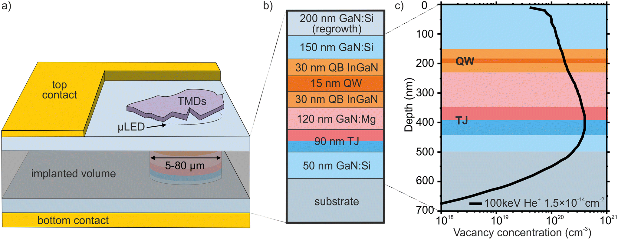 | ||
| Fig. 1 (a) Schematic of the hybrid (In,Ga)N μ-LED/TMD-monolayer device. (b) Sketch of the nitride μ-LED structure grown by plasma-assisted molecular beam epitaxy, with a characteristic sequence of epitaxial sections. (c) Ion-implantation profile for the implemented He+ energy of 100 keV and a dose of 1.5 × 1014 cm−2. | ||
After ion implantation, the regrowth of 200 nm highly conductive n-type GaN enhances current spread at the top of μ-LEDs and allows the creation of the side contacts to the device. After regrowth, the 150 × 300 μm devices containing arrays of individual microdevices were separated by reactive-ion etching. Next, on the Ga-polar side of the samples, the Ti/Al/Ni/Au metal contact was deposited with a photolithographic mask, followed by lift-off. The same metal contacts were used for bottom contact on the nitrogen polar side.
The TMD monolayers were placed on top of the (In,Ga)N μ-LEDs (Fig. 1a) using deterministic transfer procedures. Monolayer flakes were mechanically exfoliated from bulk crystals with a chemically pure backgrinding tape and transferred to the μ-LED surface using Gel-Pak DGL-X4 elastomeric films. A number of devices were prepared, comprising different MoS2, MoSe2, WSe2 and WS2 monolayers.
The optical measurements were carried out in two experimental configurations. Time-integrated studies were performed with the samples placed in the cold-finger cryostat. The emission of TMD monolayers was measured in two different configurations. Primarily, the measurements were carried out using external laser excitation at 532 nm (2330 meV). Secondly, the luminescence was triggered from underneath with (In,Ga)N μ-LEDs.
The spectra composed of sharp emission lines characteristic of a WSe2 monolayer were also examined with photon correlation experiments. These experiments were carried out in the Hanbury–Brown–Twiss configuration, under (In,Ga)N LED excitation, and required the device to be immersed in superfluid helium to minimize the undesirable effects of heating (when large currents are driven to trigger the (In,Ga)N LEDs).
3. Results and discussion
The optical microscopy images of the WSe2, MoSe2, WS2 and MoS2 monolayers deposited on top of individual (In,Ga)N μ-LEDs are illustrated in Fig. 2a–d. The characteristic, low temperature (10 K) microluminescence spectra of these layers are shown, correspondingly, in Fig. 2e–h. The spectra shown with blue traces were measured under excitation with the external laser (532 nm), whereas those shown in red were activated by the underneath (In,Ga)N μ-LEDs. The photoluminescence signals measured under external excitation are typical (with respect to spectral shapes and characteristic energies and intensities) of TMD monolayers, as often studied when they are directly deposited on conventional Si/SiO2 substrates. The characteristic spectra of our WSe2, MoSe2 and WS2 monolayers are fairly well reproduced when they are excited with (In,Ga)N μ-LEDs. On the other hand, the apparent background signal (see dashed traces in Fig. 2e and f), which is due to an unfiltered low-energy tail of the (In,Ga)N emission, largely distorts the spectrum of the MoS2 monolayer. This is, in fact, because of the rather weak luminescence efficiency of MoS2 monolayers, as commonly reported when this particular TMD monolayer is not protected by hexagonal boron nitride.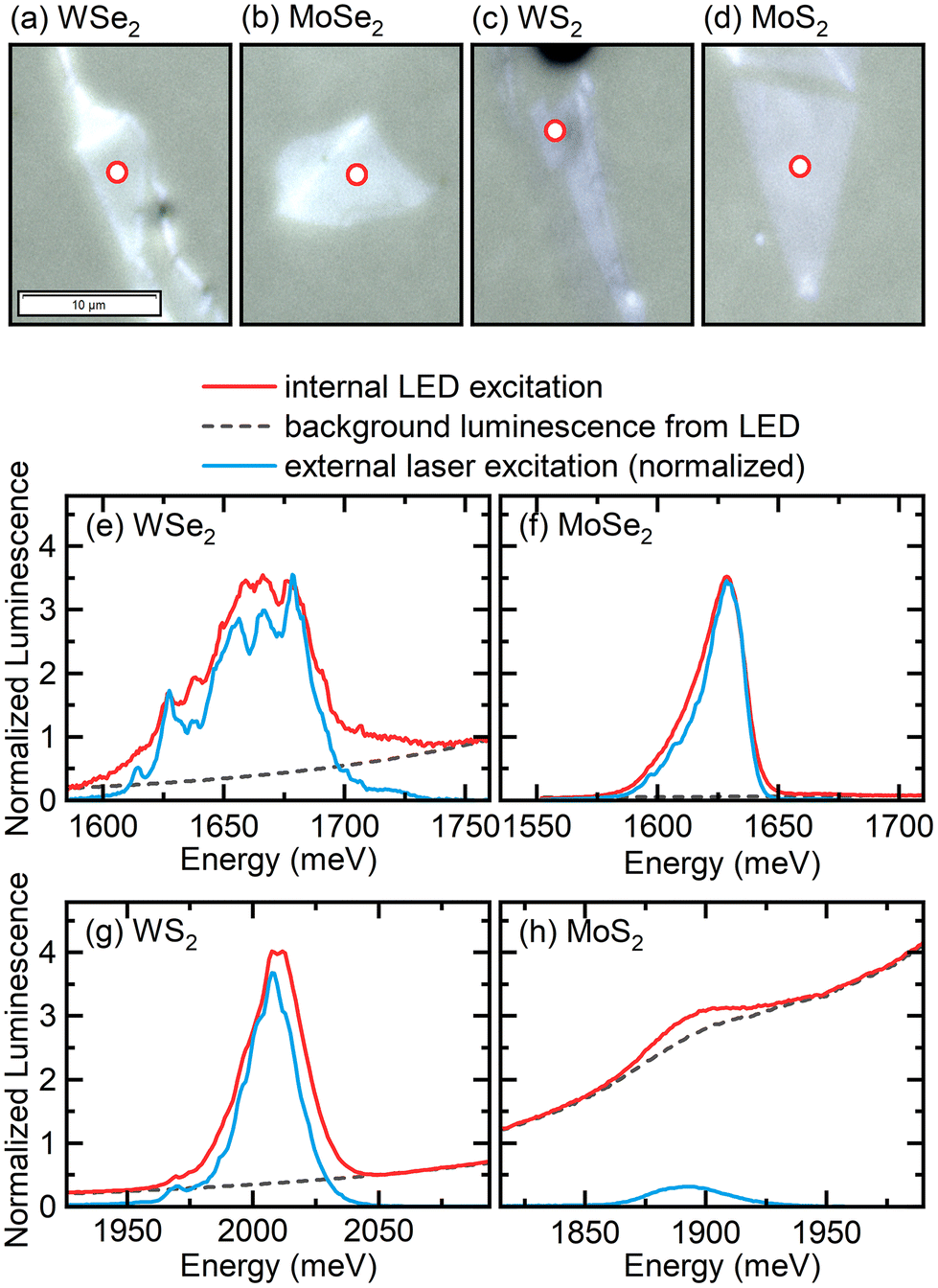 | ||
| Fig. 2 (a–d) Images of the four different monolayers of TMDs. The flakes are exfoliated on μ-LEDs, which span the whole photo area. The μ-LED current density is equal to 0.3 μA μm−2. Red circles mark the area from which the luminescence was acquired. (e–h) Spectra of the monolayers acquired under μ-LED excitation (red) and 532 nm (2330 meV) external laser excitation (blue). Dashed line: μ-LED luminescence acquired at the off-flake spot of the sample. | ||
Having established the overall functionality of our pseudo-electroluminescence devices, we now turn our attention to structures displaying sharp emission lines, possibly comprising the quantum emitter centers. Such centers can emerge in several different TMDs, but they preferentially appear in WSe2 layers,39 which we chose for further development. Several μ-(In,Ga)N-LED/WSe2-monolayer devices were prepared and tested. The irregular shape of WSe2 flakes was found to favour the observation of sharp emission lines. One may speculate that this is due to the increased probability of the formation of specific centers trapping the photoexcited carriers at the edges of TMD flakes9,10 or induced by inhomogeneous strain distribution.11–15
The representative example of a device displaying sharp emission lines contains a narrow, elongated flake of a WSe2 monolayer. The device was mounted on a cold finger of the cryostat, cooled down to 10 K and primarily tested under such conditions. After turning on the (In,Ga)N diodes, the emission spectra, in the spectral range 1590–1775 meV, were recorded when scanning the surface of the WSe2 flake and its surroundings with a spatial resolution of 2 μm. A map of the intensity of the PL integrated over the spectral range of 1625–1640 meV is shown in Fig. 3a. This image illustrates well the shape of the flake that extends over the active areas of two neighbouring (In,Ga)N μ-LEDs. The background signal due to the emission tail of the (In,Ga)N diode is fairly weak—see the spectrum measured outside the flake area (Fig. 3b). The spectra measured in the areas in the middle of the flake, away from its edges, exhibit a broad feature centered at 1660 meV—a typical response of the WSe2 ML with significant spatial inhomogeneity (Fig. 3b). However, near the edges and narrow parts of the flake, the luminescence spectra often display sharp lines (Fig. 3c).
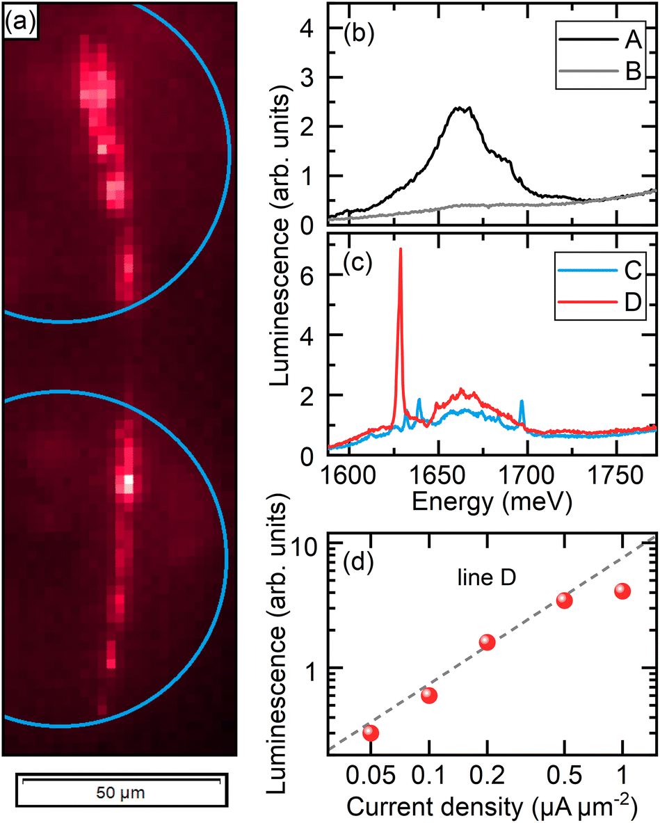 | ||
| Fig. 3 (a) Map of the luminescence of a long and narrow flake of a monolayer WSe2. The signal is integrated over the 1625–1640 meV range at a μ-LED current density of 0.5 μA μm−2. Blue circles mark the outlines of the two circular μ-LEDs. Symbols A–D mark the spots presented in panels (b and c). (b) μ-LED excited PL of the homogeneous part of the WSe2 flake (black) and the background luminescence of the μ-LED (grey). (c) μ-LED excited PL from the two spots with the narrow-line emitters. (d) The dependence of the luminescence intensity of line D on the μ-LED current density. The excitation sublinearity is caused by the elevated sample surface temperature at the highest current densities. | ||
Notably, the low activation current (below 1 nA μm−2) of our device permits measurement of the emission spectra of the WSe2 monolayer over a broad range of current densities driving the (In,Ga)N diodes and thus enables the straightforward tuning of the excitation power to match the saturation point of a particular emitter. To illustrate this effect, we present a typical PL intensity of the emitter as a function of the current density (Fig. 3d). As the luminescence intensity of the narrow lines in the WSe2 monolayers is known to drop down upon increasing the temperature,40 we conclude that the observed effect is likely due to the low cooling efficiency of our device under the current arrangement (limited by the heat transfer effectiveness between our device and the mounting base in the cryostat). However, the positioning of the μ-LED directly beneath the substrate surface limits the thermal performance of the device at very high excitation powers when compared to equivalent external laser excitation. The heat generation process can be suppressed by reducing the size of the μ-LED and precise positioning of the TMD flakes. Alternatively, if only low-duty-cycle operation is required, much higher instantaneous powers are feasible.
To demonstrate the operation of our device as a single-photon source, the device was immersed in a superfluid helium bath and cooled down to a temperature of 1.65 K. This resulted in the improved cooling efficiency of the device, enabling the application of higher diode currents, and at the same time gaining higher emission intensities of narrow emission lines. This allowed for the correlation measurements of the photon statistics emitted from the particular centre.
Fig. 4a presents the spectrum of the narrow line emitter in the WSe2 monolayer under (In,Ga)N μ-LED excitation that was powered with 1.8 μA μm−2 current. We note the particularly low ratio of the background μ-LED spectral tail of the narrow emission line intensity. Any uncorrelated photons detected in the Hanbury–Brown–Twiss experiment would proportionally reduce the amplitude of the coincidence dip as well as the feasibility of our device as a single-photon source.
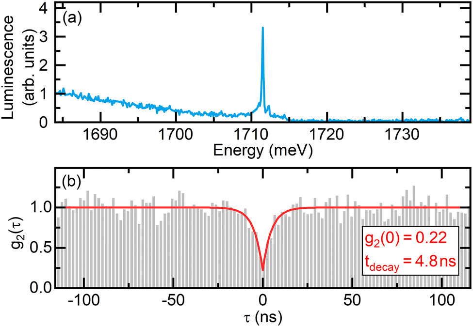 | ||
| Fig. 4 (a) Luminescence spectrum of the narrow emission line chosen for the single-photon correlation experiment. (b) Coincidence correlation counts as a function of the time interval between photons. The photoluminescence is excited with μ-LED. The broad background luminescence from the μ-LED was not subtracted in post-processing. | ||
The acquired photon coincidence correlation function, g2(τ), is presented in Fig. 4b. The photon coincidence correlation function g2(τ) denotes the relative probability density of an event with a time separation τ. The decrease in the g2 value around τ = 0 evidences the single-photon component of the emission. The emission has predominantly single-photon characteristics when g2(0) < 0.5.
The amplitude of the correlation function at zero delay is significantly low (g2(0) = 0.22), which attests to the single-photon character of the emission. The photon coincidence correlation can also be used to determine the lifetime of the emitter state (Fig. 4b). The lifetime is equal to the characteristic decay time of the antibunching feature in the g2(τ) profile at the low photon rate limit. The lifetime obtained in our experiment (tdecay = 4.8 ns) is in agreement with the results obtained in other studies.9,13,41–43
We also used the photon coincidence correlation experiment to verify the temporal stability of the emitter. Fluctuations of either the emitter intensity or the intensity of its excitation source would result in photon bunching. We observed no decrease in g2 at large τ, confirming the good stability of the emission center and the μ-LEDs. The spectral wandering of the emission line was confined within 1 meV from the central position, similar to emitters in WSe2/SiO2 structures.9,44–46 We also observed good long-term stability of our device, evidencing the advantage of the μ-LED excitation over multimodal semiconductor laser excitation. During several days of measurements, we observed no significant variation in the emission efficiency, emission energy or line shape of the selected center.
4. Conclusion
In conclusion, we have demonstrated that light emission from TMD monolayers can be efficiently generated when they are directly deposited on and excited by (In,Ga)N μ-LEDs. Our hybrid devices, 100 μm in size, can be seen as an optional route for effective, electrically driven generation of light from TMD semiconductors. The devices equipped with different MoS2, WSe2, WS2 and MoSe2 monolayers have been shown to be operational at low temperatures, thanks to the unique design of our (In,Ga)N micro-LEDs. A proof of concept for a new, electrically driven source of single photons has been demonstrated with one of our (In,Ga)N μ-LEDs/WSe2-monolayer devices.Conflicts of interest
There are no conflicts to declare.Acknowledgements
This work is supported by the TEAM-TECH POIR.04.04.00-00-210C/16-00 and TEAM POIR.04.04.00-00-1A18/16-01 (ATOMOPTO) projects of the Foundation for Polish Science co-financed by the European Union under the European Regional Development Fund. This work was supported by the National Science Centre, Poland under project 2021/41/N/ST3/04240. A. R. acknowledges support from the “Diamentowy Grant” under decision DI2017/008347 of Ministry of Education and Science of Poland. The work was also supported by the EU Graphene Flagship project.References
- Y. You, X.-X. Zhang, T. C. Berkelbach, M. S. Hybertsen, D. R. Reichman and T. F. Heinz, Nat. Phys., 2015, 11, 477 Search PubMed.
- K. He, N. Kumar, L. Zhao, Z. Wang, K. F. Mak, H. Zhao and J. Shan, Phys. Rev. Lett., 2014, 113, 026803 CrossRef CAS PubMed.
- J. S. Ross, S. Wu, H. Yu, N. J. Ghimire, A. M. Jones, G. Aivazian, J. Yan, D. G. Mandrus, D. Xiao and W. Yao, et al. , Nat. Commun., 2013, 4, 1474 CrossRef PubMed.
- E. Lorchat, S. Azzini, T. Chervy, T. Taniguchi, K. Watanabe, T. W. Ebbesen, C. Genet and S. Berciaud, ACS Photonics, 2018, 5, 5047–5054 CrossRef CAS.
- K. F. Mak, C. Lee, J. Hone, J. Shan and T. F. Heinz, Phys. Rev. Lett., 2010, 105, 136805 CrossRef PubMed.
- A. Splendiani, L. Sun, Y. Zhang, T. Li, J. Kim, C.-Y. Chim, G. Galli and F. Wang, Nano Lett., 2010, 10, 1271–1275 CrossRef CAS PubMed.
- H. Zeng, J. Dai, W. Yao, D. Xiao and X. Cui, Nat. Nanotechnol., 2012, 7, 490 CrossRef CAS PubMed.
- K. F. Mak, K. He, J. Shan and T. F. Heinz, Nat. Nanotechnol., 2012, 7, 494 CrossRef CAS PubMed.
- M. Koperski, K. Nogajewski, A. Arora, V. Cherkez, P. Mallet, J.-Y. Veuillen, J. Marcus, P. Kossacki and M. Potemski, Nat. Nanotechnol., 2015, 10, 503 CrossRef CAS PubMed.
- P. Tonndorf, R. Schmidt, R. Schneider, J. Kern, M. Buscema, G. A. Steele, A. Castellanos-Gomez, H. S. van der Zant, S. M. de Vasconcellos and R. Bratschitsch, Optica, 2015, 2, 347–352 CrossRef CAS.
- M. Brooks and G. Burkard, Phys. Rev. B, 2018, 97, 195454 CrossRef CAS.
- J. Kern, I. Niehues, P. Tonndorf, R. Schmidt, D. Wigger, R. Schneider, T. Stiehm, S. Michaelis de Vasconcellos, D. E. Reiter and T. Kuhn, et al. , Adv. Mater., 2016, 28, 7101–7105 CrossRef CAS PubMed.
- S. Kumar, A. Kaczmarczyk and B. D. Gerardot, Nano Lett., 2015, 15, 7567–7573 CrossRef CAS PubMed.
- A. Branny, S. Kumar, R. Proux and B. D. Gerardot, Nat. Commun., 2017, 8, 15053 CrossRef CAS PubMed.
- Y. Luo, N. Liu, X. Li, J. C. Hone and S. Strauf, 2D Mater., 2019, 6, 035017 CrossRef CAS.
- M. Blauth, M. Jürgensen, G. Vest, O. Hartwig, M. Prechtl, J. Cerne, J. J. Finley and M. Kaniber, Nano Lett., 2018, 18, 6812–6819 CrossRef CAS PubMed.
- F. Peyskens, C. Chakraborty, M. Muneeb, D. Van Thourhout and D. Englund, Nat. Commun., 2019, 10, 4435 CrossRef PubMed.
- J. Wang, I. Verzhbitskiy and G. Eda, Adv. Mater., 2018, 30, 1802687 CrossRef PubMed.
- H. Qiu, T. Xu, Z. Wang, W. Ren, H. Nan, Z. Ni, Q. Chen, S. Yuan, F. Miao, F. Song, G. Long, Y. Shi, L. Sun, J. Wang and X. Wang, Nat. Commun., 2013, 4, 2642 CrossRef PubMed.
- S. Wang, W. Zhao, F. Giustiniano and G. Eda, Phys. Chem. Chem. Phys., 2016, 18, 4304–4309 RSC.
- C. Palacios-Berraquero, M. Barbone, D. M. Kara, X. Chen, I. Goykhman, D. Yoon, A. K. Ott, J. Beitner, K. Watanabe, T. Taniguchi, A. C. Ferrari and M. Atatüre, Nat. Commun., 2016, 7, 12978 CrossRef CAS PubMed.
- R. S. Sundaram, M. Engel, A. Lombardo, R. Krupke, A. C. Ferrari, P. Avouris and M. Steiner, Nano Lett., 2013, 13, 1416–1421 CrossRef CAS PubMed.
- Y. Ye, Z. Ye, M. Gharghi, H. Zhu, M. Zhao, Y. Wang, X. Yin and X. Zhang, Appl. Phys. Lett., 2014, 104, 193508 CrossRef.
- R. Cheng, D. Li, H. Zhou, C. Wang, A. Yin, S. Jiang, Y. Liu, Y. Chen, Y. Huang and X. Duan, Nano Lett., 2014, 14, 5590–5597 CrossRef CAS PubMed.
- F. Withers, O. Del Pozo-Zamudio, A. Mishchenko, A. P. Rooney, A. Gholinia, K. Watanabe, T. Taniguchi, S. J. Haigh, A. K. Geim, A. I. Tartakovskii and K. S. Novoselov, Nat. Mater., 2015, 14, 301–306 CrossRef CAS PubMed.
- S. Wang, J. Wang, W. Zhao, F. Giustiniano, L. Chu, I. Verzhbitskiy, J. Zhou Yong and G. Eda, Nano Lett., 2017, 17, 5156–5162 CrossRef CAS PubMed.
- D. Li, R. Cheng, H. Zhou, C. Wang, A. Yin, Y. Chen, N. O. Weiss, Y. Huang and X. Duan, Nat. Commun., 2015, 6, 7509 CrossRef PubMed.
- T. Wu, C.-W. Sher, Y. Lin, C.-F. Lee, S. Liang, Y. Lu, S.-W. Huang Chen, W. Guo, H.-C. Kuo and Z. Chen, Appl. Sci., 2018, 8, 1557 CrossRef.
- W. Pacuski, M. Grzeszczyk, K. Nogajewski, A. Bogucki, K. Oreszczuk, J. Kucharek, K. E. Połczyńska, B. Seredyński, A. Rodek, R. Bożek, T. Taniguchi, K. Watanabe, S. Kret, J. Sadowski, T. Kazimierczuk, M. Potemski and P. Kossacki, Nano Lett., 2020, 20, 3058–3066 CrossRef CAS PubMed.
- J. Day, J. Li, D. Y. C. Lie, C. Bradford, J. Y. Lin and H. X. Jiang, Appl. Phys. Lett., 2011, 99, 031116 CrossRef.
- S. Chen, J. Li, Z. Guo, L. Chen, K. Wen, P. Xu, J. Yang and Y. Qin, J. Phys. D: Appl. Phys., 2021, 55, 115105 CrossRef.
- C. Skierbiszewski, H. Turski, M. Zak, K. Nowakowski-Szkudlarek, G. Muziol, M. Siekacz, A. Feduniewicz-Zmuda and M. Sawicka, 2018 76th Device Research Conference (DRC), 2018, pp. 1–2.
- S. J. Kowsz, E. C. Young, B. P. Yonkee, C. D. Pynn, R. M. Farrell, J. S. Speck, S. P. DenBaars and S. Nakamura, Opt. Express, 2017, 25, 3841–3849 CrossRef CAS PubMed.
- C. Skierbiszewski, G. Muziol, K. Nowakowski-Szkudlarek, H. Turski, M. Siekacz, A. Feduniewicz-Zmuda, A. Nowakowska-Szkudlarek, M. Sawicka and P. Perlin, Appl. Phys. Express, 2018, 11, 034103 CrossRef.
- M. Chlipala, H. Turski, M. Siekacz, K. Pieniak, K. Nowakowski-Szkudlarek, T. Suski and C. Skierbiszewski, Opt. Express, 2020, 28, 30299–30308 CrossRef CAS PubMed.
- S. Bharadwaj, K. Lee, K. Nomoto, A. Hickman, L. van Deurzen, V. Protasenko, H. G. Xing and D. Jena, Appl. Phys. Lett., 2020, 117, 031107 CrossRef CAS.
- M. Chlipała, H. Turski, M. Żak, G. Muziol, M. Siekacz, K. Nowakowski-Szkudlarek, N. Fiuczek, A. Feduniewicz-Żmuda, J. Smalc-Koziorowska and C. Skierbiszewski, Appl. Phys. Lett., 2022, 120, 171104 CrossRef.
- J. Slawinska, G. Muziol, M. Siekacz, H. Turski, M. Hajdel, M. Zak, A. Feduniewicz-Zmuda, G. Staszczak and C. Skierbiszewski, Opt. Express, 2022, 30, 27004–27014 CrossRef CAS PubMed.
- C. Chakraborty, N. Vamivakas and D. Englund, Nanophotonics, 2019, 8, 2017–2032 Search PubMed.
- K. Oreszczuk, T. Kazimierczuk, T. Smoleńński, K. Nogajewski, M. Grzeszczyk, A. Łopion, M. Potemski and P. Kossacki, Phys. Rev. B, 2020, 102, 245409 CrossRef CAS.
- A. Srivastava, M. Sidler, A. V. Allain, D. S. Lembke, A. Kis and A. Imamoğlu, Nat. Nanotechnol., 2015, 10, 491 CrossRef CAS PubMed.
- Y.-M. He, G. Clark, J. R. Schaibley, Y. He, M.-C. Chen, Y.-J. Wei, X. Ding, Q. Zhang, W. Yao and X. Xu, et al. , Nat. Nanotechnol., 2015, 10, 497 CrossRef CAS PubMed.
- C. Chakraborty, L. Kinnischtzke, K. M. Goodfellow, R. Beams and A. N. Vamivakas, Nat. Nanotechnol., 2015, 10, 507 CrossRef CAS PubMed.
- A. Srivastava, M. Sidler, A. V. Allain, D. S. Lembke, A. Kis and A. Imamoğlu, Nat. Nanotechnol., 2015, 10, 491 CrossRef CAS PubMed.
| This journal is © The Royal Society of Chemistry 2022 |